International Airport Industrial Park • Mailing Address: PO Box 11400, Tucson, AZ 85734 • Street Address: 6730 S. Tucson Bl vd., Tucson, AZ 85706 • Tel: (520) 746-1111Twx: 910-952-1111 • Internet: http://www.burr-brown.com/ • Cable: BBRCORP • Telex: 066-6491 • FAX: (520) 889-1510 • I mmediate Product Info: (800) 548-6132
FEATURES 16-BIT DELTA-SIGMA DAC AND ADC DESIGNED FOR MODEM ANALOG FRONT END:
Supports up to 56kbps Operation ANALOG PERFORMANCE:
Sampling Frequency: 7.2kHz to 26kHzDynamic Range: 88dB (typ) at f S = 8kHz, fIN = 1kHz
SYSTEM CLOCK: 512f S
MASTER OR SLAVE OPERATION ON-CHIP CRYSTAL OSCILLATOR CIRCUIT ADC-TO-DAC LOOP-BACK MODE TIME SLOT MODE SUPPORTS UP TO
FOUR CODECs ON A SINGLE SERIALINTERFACE
POWER-DOWN MODE: 60µA (typ)
DESCRIPTIONThe PCM3500 is a low cost, 16-bit CODEC designedfor modem Analog Front End (AFE) and speech pro-cessing applications. The PCM3500’s low power op-eration from +2.7V to +3.6V power supplies, alongwith an integrated power-down mode, make it ideal forportable applications.
The PCM3500 integrates all of the functions needed fora modem or voice CODEC, including delta-sigma
digital-to-analog and analog-to-digital converters, in-put anti-aliasing filter, digital high-pass filter for DCblocking, and an output low-pass filter. The synchro-nous serial interface provides for a simple, or glue-freeinterface to popular DSP and RISC processors. Theserial interface also supports Time Division Multiplex-ing (TDM), allowing up to four CODECs to share asingle 4-wire serial bus.
PCM3500
InterpolationDigital Filter
Mode Control
DecimationDigital Filter
Reference
AAF HPF
M/SHPFD TSC XTIXTOLOOP
VREF1
VCOM
VREF2
VIN
AGND
Ser
ial I
/O In
terf
ace
PDWN
Power
DGNDAGND VDDVCC
Loop
FS
BCK
DIN
DOUT
FSO
SCKIOClockGen/OSC
∆ΣModulator
(ADC)
∆ΣModulator
SMF
VOUT
AGND
Multi-LevelDAC
POWER SUPPLY: Single +2.7V to +3.6V SMALL PACKAGE: SSOP-24
For most current data sheet and other productinformation, visit www.burr-brown.com
SBAS117
®
2PCM3500
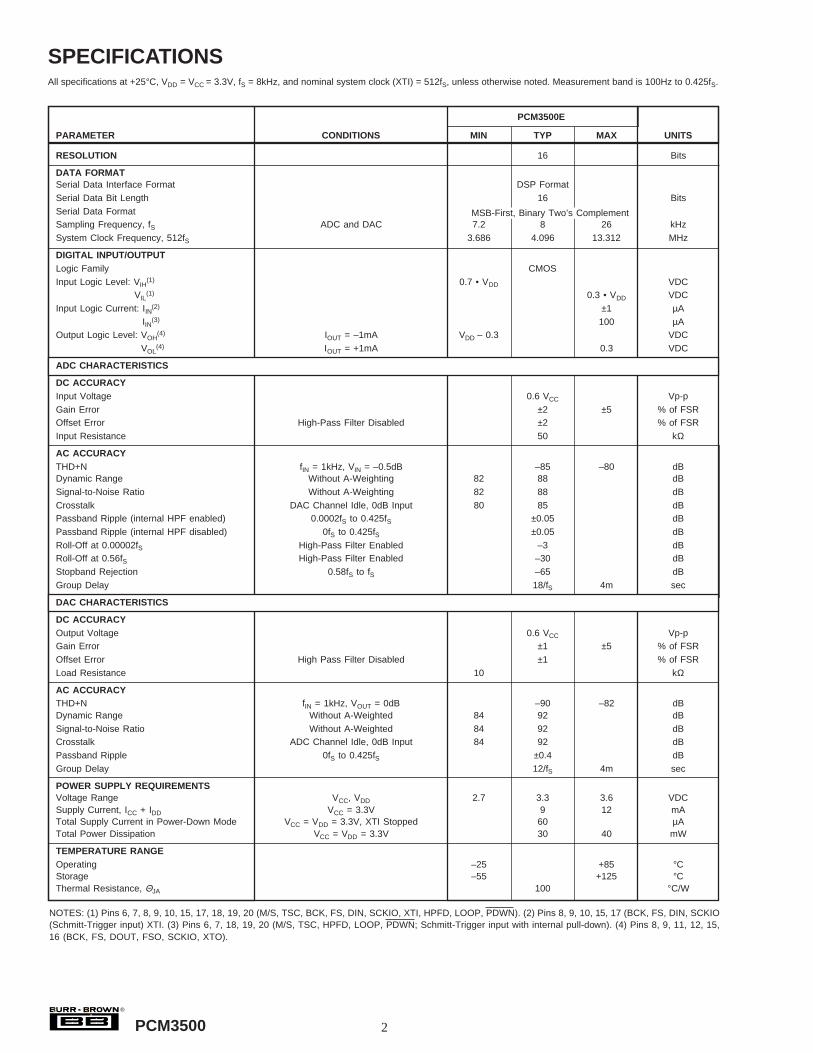
SPECIFICATIONSAll specifications at +25°C, VDD = VCC = 3.3V, fS = 8kHz, and nominal system clock (XTI) = 512fS, unless otherwise noted. Measurement band is 100Hz to 0.425fS.
DATA FORMATSerial Data Interface Format DSP FormatSerial Data Bit Length 16 BitsSerial Data FormatSampling Frequency, fS ADC and DAC 7.2 8 26 kHzSystem Clock Frequency, 512fS 3.686 4.096 13.312 MHz
DIGITAL INPUT/OUTPUTLogic Family CMOSInput Logic Level: VIH
The information provided herein is believed to be reliable; however, BURR-BROWN assumes no responsibility for inaccuracies or omissions. BURR-BROWN assumes noresponsibility for the use of this information, and all use of such information shall be entirely at the user’s own risk. Prices and specifications are subject to change without notice.No patent rights or licenses to any of the circuits described herein are implied or granted to any third party. BURR-BROWN does not authorize or warrant any BURR-BROWNproduct for use in life support devices and/or systems.
Supply Voltage Differences ............................................................... ±0.1V
GND Voltage Differences .................................................................. ±0.1VDigital Input Voltage ................................................... –0.3V to VDD + 0.3V
Input Current (any pins except supply) ........................................... ±10mA
Power Dissipation .......................................................................... 300mW
Operating Temperature Range ......................................... –25°C to +85°C
Storage Temperature ...................................................... –55°C to +125°C
Junction Temperature ...................................................................... 150°C
Lead Temperature (soldering, 5s) .................................................. +260°C
ABSOLUTE MAXIMUM RATINGS ELECTROSTATICDISCHARGE SENSITIVITY
This integrated circuit can be damaged by ESD. Burr-Brownrecommends that all integrated circuits be handled withappropriate precautions. Failure to observe proper handlingand installation procedures can cause damage.
ESD damage can range from subtle performance degrada-tion to complete device failure. Precision integrated circuitsmay be more susceptible to damage because very smallparametric changes could cause the device not to meet itspublished specifications.
PACKAGE SPECIFIEDDRAWING TEMPERATURE PACKAGE ORDERING TRANSPORT
PRODUCT PACKAGE NUMBER RANGE MARKING NUMBER (1) MEDIA
PCM3500E 24-Lead SSOP 338 –25°C to +85°C PCM3500E PCM3500E Rails" " " " " PCM3500E/2K Tape and Reel
NOTES: (1) Models with a slash (/) are available only in Tape and Reel in the quantities indicated (e.g., /2K indicates 2000 devices per reel). Ordering 2,000 piecesof “PCM3500E/2K” will get a single 2000-piece Tape and Reel.
PACKAGE/ORDERING INFORMATION
®
4PCM3500
PIN CONFIGURATION
Top View SSOP
PIN NAME I/O DESCRIPTION
1 VCOM OUT Common-Mode Voltage (0.5VCC). This pin should be connected to ground through a capacitor.
2 VREF1 — Decouple Pin for Reference Voltage 1 (0.99VCC). This pin should be connected to ground through a capacitor.
3 VREF2 — Decouple Pin for Reference Voltage 2 (0.2VCC). This pin should be connected to ground through a capacitor.
4 VIN IN Analog Input for the ADC.
5 AGND — Analog Ground for the ADC Input Signal.
6 M/S IN Master/Slave Select. This pin is used to determine the operating mode for the serial interface. A logic ‘0’ on this pin selects the SlaveMode. A logic ‘1’ on this pin selects the Master Mode.(2)
7 TSC IN Time Slot Mode Control. This pin is used to select the time slot operating mode. A logic ‘0’ on this pin disables Time Slot Mode. Alogic ‘1’ on this pin enables Time Slot Mode.(2)
8 BCK I/O Bit Clock. This pin serves as the bit (or shift) clock for the serial interface. This pin is an input in Slave Mode and an output in MasterMode.(1)
9 FS I/O Frame Sync. This pin serves as the frame synchronization clock for the serial interface. This pin is an input in Slave Mode and anoutput in Master Mode.(1)
10 DIN IN Serial Data Input. This pin is used to write 16-bit data to the DAC.(1)
11 DOUT OUT Serial Data Output. The ADC outputs 16-bit data on this pin.(3)
12 FSO OUT Frame Sync Output. Active only when Time Slot Mode is enabled. This pin is set to a high impedance state when Time Slot modeis disabled (TSC = 0).
13 VDD — Digital Power Supply. Used to power the digital section of the ADC and DAC, as well as the serial interface and mode control logic.This pin is not internally connected to VCC.
14 DGND — Digital Ground. Internally connected through the substrate to analog ground.
15 SCKIO I/O System Clock Input/Output. This pin is a system clock output when using the crystal oscillator or XTI as the system clock input; whenXTI is connected to ground, this pin is a system clock input.(1)
16 XTO OUT Crystal Oscillator Output.
17 XTI IN Crystal Oscillator Input or an External System Clock Input.
18 HPFD IN High-Pass Filter Disable. When this pin is set to a logic ‘1’, the HPF function in the ADC is disabled.(2)
19 LOOP IN ADC-to-DAC Loop-Back Control. When this pin is set to logic ‘1’, the ADC data is fed to the DAC input.(2)
20 PDWN IN Power Down and Reset Control. When this pin is logic ‘0’, Power-Down Mode is enabled. The PCM3500 is reset on the rising edgeof this signal.(2)
21 AGND — Analog Ground for the DAC Output Signal.
22 VOUT OUT Analog Output from the DAC Output Filter.
23 AGND — Analog Ground. This is the ground for the internal analog circuitry.
24 VCC — Analog Power Supply. Used to power the analog circuitry of the ADC and DAC.
NOTES: (1) Schmitt-Trigger input. (2) Schmitt-Trigger input with an internal pull-down resistor. (3) Tri-state output in Time Slot Mode.
SYSTEM CLOCK AND RESET/POWER DOWNSYSTEM CLOCK INPUT AND OUTPUT
The PCM3500 requires a system clock for operating thedigital filters and delta-sigma data converters.
The system clock may be supplied from an external masterclock or generated using the on-chip crystal oscillator cir-cuit. Figure 1 shows the required connections for externaland crystal clock operation. The system clock must operateat 512 times the sampling frequency, fS, with samplingfrequencies from 7.2kHz to 26kHz. This gives an effectivesystem clock frequency range of 3.6864MHz to 13.312MHz.
Table I shows system clock frequencies for common sam-pling frequencies.
For external clock operation, XTI (pin 17) or SCKIO (pin 15)is driven by a master clock source. If SCKIO is used as thesystem clock input, then XTI must be connected to ground.
SAMPLING FREQUENCY (kHz) SYSTEM CLOCK FREQUENCY (MHz)
8 4.09611.025 5.6448
16 8.19222.05 11.2896
24 12.288
TABLE I. System Clock Frequencies for Common Sam-pling Frequencies.
FIGURE 1. System Clock Generation.
For either case, XTO (pin 16) should be left open. The systemclock source should be free of noise and exhibit low phasejitter in order to obtain optimal dynamic performance fromthe PCM3500. Figure 2 shows the system clock timingrequirements associated with an external master clock.
For crystal oscillator operation, a crystal is connected be-tween XTI (pin 17) and XTO (pin 16), along with thenecessary load capacitors (10pF to 33pF per pin, as shownin Figure 1). A fundamental-mode, parallel resonant crystalis required.
FIGURE 2. External System Clock Timing Requirements.
C1
C2
C1, C2 = 10pF to 33pF
XTI
R
Crystal
XTO
PCM3500
SCKIO
CRYSTAL RESONATORCONNECTION
ExternalClock
ExternalClock
XTI
XTO
R
PCM3500
EXTERNAL CLOCK INPUT-XTI(XTO must be open)
SCKIO
XTI
XTO
R
PCM3500
EXTERNAL CLOCK INPUT-SCKIO(XTO must be open)
SCKIO
System Clock Pulse Width HIGH tCLKIH 20ns (min)
System Clock Pulse Width LOW tCLKIL 20ns (min)
tCLKIH
tCLKIL 1/512fS
0.7VDD"H"XTI
orSCKIO "L" 0.3VDD
®
13 PCM3500
Reset and Power Down
The PCM3500 supports power-on reset, external reset, andpower-down operations. Power-on reset is performed byinternal circuitry automatically at power up, while the exter-nal reset is initiated using the PDWN input (pin 20).
Power-on reset occurs when power and system clock areinitially applied to the PCM3500. The internal reset cir-cuitry requires that the system clock be active at power up,with at least three system clock cycles occurring prior toVDD = 2.2V. When VDD exceeds 2.2V, the power-on resetcomparator enables the initialization sequence, which re-quires 1024 system clock periods for completion. Duringthe initialization sequence, the DAC output is forced toAGND, and the ADC output is forced to a high impedancestate. After the initialization sequence has completed, theDAC and ADC outputs experience a delay before theyoutput a valid signal or data. Refer to Figures 3 and 5 forpower-on reset and post-reset delay timing.
External reset is performed by first setting PDWN = ‘0’ andthen setting PDWN = ‘1’. The LOW to HIGH transition on
PDWN causes the reset initialization sequence to start.During the initialization sequence, the DAC output is forcedto AGND, and the ADC output is forced to a high impedancestate. After the initialization sequence has completed, theDAC and ADC outputs experience a delay before theyoutput a valid signal or data. Refer to Figures 4 and 5 forexternal reset and post-reset delay timing.
Power-down mode is enabled by setting PDWN = ‘0’.During power-down mode, minimum current is drawn whenthe system clock is removed, resulting in 60µA (typical)power supply current. The PDWN input includes an internalpull-down resistor, which places the PCM3500 in power-down mode at power-up if the PDWN pin is left uncon-nected. Ideally, the PDWN input should be driven by activelogic in order to control reset and power-down operation. Ifthe PDWN pin is to be unused in the system application, itshould be connected to VDD to enable normal operation. Bysetting PDWN = ‘1’ when exiting power-down mode, thePCM3500 will initiate an external reset as described earlierin this section.
1024 System Clock Periods
ResetReset Removal
2.4V2.2V2.0V
VDD
Internal Reset
System Clock
FIGURE 3. Power-On Reset Timing.
1024 System Clock Periods
ResetReset Removal
System Clock
Internal Reset
PDWNtRST
PWDN = LOW Pulse Width tRST = 40ns minimum
FIGURE 4. External Reset Timing.
FIGURE 5. DAC and ADC Output for Reset and Power Down.
Reset
Power Down
GNDVCOM
(0.5VCC)
Ready/OperationInternal Reset
or Power Down
ADC DOUT
DAC VOUT
High Impedance (1)
tADCDLY1 (2304/fS)
tDACDLY1 (2048/fS)
Reset Removal or Power Down OFF
NOTE: (1) The HPF transient response (exponentially attenuated signal from ±0.2% DC of FSR with 200ms time constant) appears initially.
®
14PCM3500
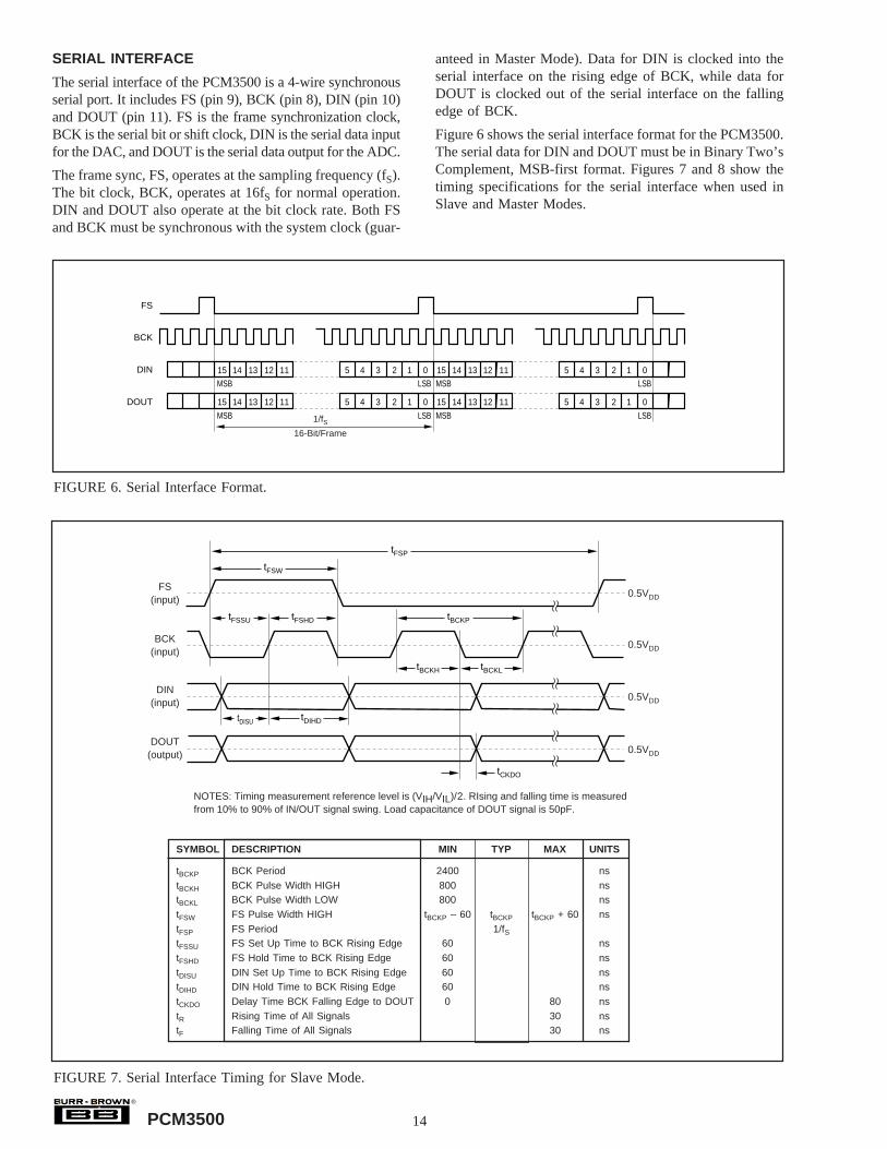
SERIAL INTERFACE
The serial interface of the PCM3500 is a 4-wire synchronousserial port. It includes FS (pin 9), BCK (pin 8), DIN (pin 10)and DOUT (pin 11). FS is the frame synchronization clock,BCK is the serial bit or shift clock, DIN is the serial data inputfor the DAC, and DOUT is the serial data output for the ADC.
The frame sync, FS, operates at the sampling frequency (fS).The bit clock, BCK, operates at 16fS for normal operation.DIN and DOUT also operate at the bit clock rate. Both FSand BCK must be synchronous with the system clock (guar-
anteed in Master Mode). Data for DIN is clocked into theserial interface on the rising edge of BCK, while data forDOUT is clocked out of the serial interface on the fallingedge of BCK.
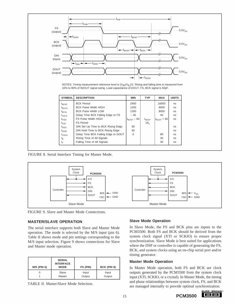
Figure 6 shows the serial interface format for the PCM3500.The serial data for DIN and DOUT must be in Binary Two’sComplement, MSB-first format. Figures 7 and 8 show thetiming specifications for the serial interface when used inSlave and Master Modes.
tBCKP BCK Period 2400 nstBCKH BCK Pulse Width HIGH 800 nstBCKL BCK Pulse Width LOW 800 nstFSW FS Pulse Width HIGH tBCKP – 60 tBCKP tBCKP + 60 nstFSP FS Period 1/fStFSSU FS Set Up Time to BCK Rising Edge 60 nstFSHD FS Hold Time to BCK Rising Edge 60 nstDISU DIN Set Up Time to BCK Rising Edge 60 nstDIHD DIN Hold Time to BCK Rising Edge 60 nstCKDO Delay Time BCK Falling Edge to DOUT 0 80 nstR Rising Time of All Signals 30 nstF Falling Time of All Signals 30 ns
FIGURE 6. Serial Interface Format.
FIGURE 7. Serial Interface Timing for Slave Mode.
tFSW
tFSSU tFSHD tBCKP
tBCKH
tDISU tDIHD
tBCKL
tCKDO
tFSP
FS(input)
BCK(input)
DIN(input)
DOUT(output)
NOTES: Timing measurement reference level is (VIH/VIL)/2. RIsing and falling time is measuredfrom 10% to 90% of IN/OUT signal swing. Load capacitance of DOUT signal is 50pF.
0.5VDD
0.5VDD
0.5VDD
0.5VDD
®
15 PCM3500
SERIALINTERFACE
M/S (PIN 6) MODE FS (PIN) BCK (PIN 8)
0 Slave Input Input1 Master Output Output
TABLE II. Master/Slave Mode Selection.
SYMBOL DESCRIPTION MIN TYP MAX UNITS
tBCKP BCK Period 2400 16000 nstBCKH BCK Pulse Width HIGH 1200 8000 nstBCKL BCK Pulse Width LOW 1200 8000 nstCKFS Delay Time BCK Falling Edge to FS – 40 40 nstFSW FS Pulse Width HIGH tBCKP – 60 tBCKP tBCKP + 60 nstFSP FS Period 1/fStDISU DIN Set Up Time to BCK Rising Edge 60 nstDIHD DIN Hold Time to BCK Rising Edge 60 nstCKDO Delay Time BCK Falling Edge to DOUT 0 80 nstR Rising Time of All Signals 30 nstF Falling Time of All Signals 30 ns
FIGURE 8. Serial Interface Timing for Master Mode.
MASTER/SLAVE OPERATION
The serial interface supports both Slave and Master Modeoperation. The mode is selected by the M/S input (pin 6).Table II shows mode and pin settings corresponding to theM/S input selection. Figure 9 shows connections for Slaveand Master mode operation.
FIGURE 9. Slave and Master Mode Connections.
Slave Mode Operation
In Slave Mode, the FS and BCK pins are inputs to thePCM3500. Both FS and BCK should be derived from thesystem clock signal (XTI or SCKIO) to ensure propersynchronization. Slave Mode is best suited for applicationswhere the DSP or controller is capable of generating the FS,BCK, and system clocks using an on-chip serial port and/ortiming generator.
Master Mode Operation
In Master Mode operation, both FS and BCK are clockoutputs generated by the PCM3500 from the system clockinput (XTI, SCKIO, or a crystal). In Master Mode, the timingand phase relationships between system clock, FS, and BCKare managed internally to provide optimal synchronization.
XTI
FS
BCK
DIN
DOUTM/S
TSC
GND
GND
Controller
SystemClock
Slave Mode
PCM3500
XTI
FS
BCK
DIN
DOUTM/S
TSC
VDD
GND
PCM3500SystemClock
Controller
Master Mode
tFSW
tCKFS tBCKP
tBCKH
tDISU tDIHD
tBCKL
tCKDO
tFSP
NOTES: Timing measurement reference level is (VIH/VIL)/2. Rising and falling time is measured from10% to 90% of IN/OUT signal swing. Load capacitance of DOUT, FS, BCK signal is 50pF.
0.5VDD
0.5VDD
0.5VDD
0.5VDD
FS(output)
BCK(output)
DIN(input)
DOUT(output)
®
16PCM3500
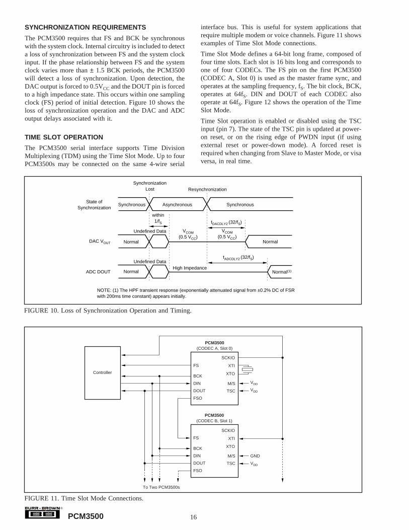
SYNCHRONIZATION REQUIREMENTS
The PCM3500 requires that FS and BCK be synchronouswith the system clock. Internal circuitry is included to detecta loss of synchronization between FS and the system clockinput. If the phase relationship between FS and the systemclock varies more than ± 1.5 BCK periods, the PCM3500will detect a loss of synchronization. Upon detection, theDAC output is forced to 0.5VCC and the DOUT pin is forcedto a high impedance state. This occurs within one samplingclock (FS) period of initial detection. Figure 10 shows theloss of synchronization operation and the DAC and ADCoutput delays associated with it.
TIME SLOT OPERATION
The PCM3500 serial interface supports Time DivisionMultiplexing (TDM) using the Time Slot Mode. Up to fourPCM3500s may be connected on the same 4-wire serial
interface bus. This is useful for system applications thatrequire multiple modem or voice channels. Figure 11 showsexamples of Time Slot Mode connections.
Time Slot Mode defines a 64-bit long frame, composed offour time slots. Each slot is 16 bits long and corresponds toone of four CODECs. The FS pin on the first PCM3500(CODEC A, Slot 0) is used as the master frame sync, andoperates at the sampling frequency, fS. The bit clock, BCK,operates at 64fS. DIN and DOUT of each CODEC alsooperate at 64fS. Figure 12 shows the operation of the TimeSlot Mode.
Time Slot operation is enabled or disabled using the TSCinput (pin 7). The state of the TSC pin is updated at power-on reset, or on the rising edge of PWDN input (if usingexternal reset or power-down mode). A forced reset isrequired when changing from Slave to Master Mode, or visaversa, in real time.
FIGURE 10. Loss of Synchronization Operation and Timing.
FIGURE 11. Time Slot Mode Connections.
Synchronous Asynchronous
SynchronizationLost Resynchronization
within1/fS
Synchronous
Normal Normal
tADCDLY2 (32/fS)
tDACDLY2 (32/fS)
VCOM(0.5 VCC)
VCOM(0.5 VCC)
State ofSynchronization
DAC VOUT
Normal Normal(1) High Impedance
ADC DOUT
NOTE: (1) The HPF transient response (exponentially attenuated signal from ±0.2% DC of FSRwith 200ms time constant) appears initially.
One Frame = 1/fS, 64 Bits per Frame, 16 Bits per Slot
CODEC C CODEC D
®
18PCM3500
SYMBOL DESCRIPTION MIN TYP MAX UNITS
tBCKP BCK Period 600 nstBCKH BCK Pulse Width HIGH 200 nstBCKL BCK Pulse Width LOW 200 nstFSW FS Pulse Width HIGH tBCKP – 60 tBCKP tBCKP + 60 nstFSP FS Period 1/fStFSSU FS Set Up TIme to BCK Rising Edge 60 nstFSHD FS Hold TIme to BCK RIsing Edge 60 nstDISU DIN Set Up Time to BCK Rising Edge 60 nstDIHD DIN Hold Time to BCK Rising Edge 60 nstCKDO Delay Time BCK Falling Edge to DOUT 0 80 nstHZDO Delay Time BCK Falling Edge to DOUT Active 20 nstDOHZ Delay Time BCK Falling Edge to DOUT Inactive 19.5 nstFSOW FSO Pulse Width HIGH tBCKP – 60 tBCKP tBCKP + 60 nstBFSO Delay Time BCK Falling Edge to FSO 0 80 nstR Rising Time of All Signals 30 nstF Falling Time of All Signals 30 ns
FIGURE 13. Serial Interface Timing for Time Slot Mode Operation (Slave Mode).
Table III shows the TSC pin settings and correspondingmode selections. When Time Slot Mode is enabled, FSO(pin 12) is used as a frame sync output, which is connectedto the FS input of the next PCM3500 in the Time Slotsequence. Figures 13 and 14 provide detailed timing forTime Slot Mode operation.
TSC (PIN 7) TIME SLOT MODE
0 Time Slot Mode Disabled, Normal Operation1 Time Slot Operation Enable
LOOP (PIN 19) LOOP-BACK MODE
0 Loop-Back Mode Disabled, Normal Operation1 Loop-Back Mode Enabled
TABLE IV. Loop-Back Mode Selection.
TABLE III. Time Slot Mode Selection.
HPFD (PIN 18) HIGH-PASS FILTER MODE
0 High-Pass Filter On1 High-Pass Filter Off
TABLE V. High-Pass Filter Mode Selection.
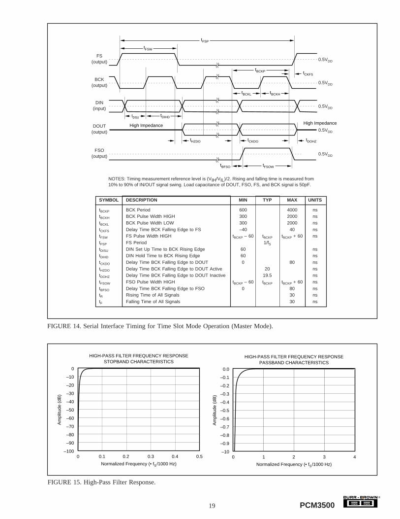
HIGH-PASS FILTER
The PCM3500 includes a digital high-pass filter in the ADCwhich may be used to remove the DC offset created by theanalog front-end (AFE) section. The high-pass filter responseis shown in Figure 15. The high-pass filter may be enabled ordisabled using the HPFD input (pin 18). Table V shows theHPFD pin settings and corresponding mode selections.
ADC-TO-DAC LOOP BACK
The PCM3500 includes a Loop-Back Mode, which directlyfeeds the ADC data to the DAC input. This mode is designedfor diagnostic testing and system adjustment. Loop-BackMode is enabled and disabled using the LOOP input (pin19). Table IV shows the LOOP pin settings and correspond-ing mode selections. The serial interface continues to oper-
ate in Loop-Back Mode, allowing the host to read the ADCdata at the DOUT pin.
tFSW
tFSSU
High Impedance High Impedance
tFSHD tBCKP
tBCKL
tDISU tDIHD
tBCKH
tCKDOtHZDO tDOHZ
tFSP
NOTES: Timing measurement reference level is (VIH/VIL)/2. Rising and falling time is measured from10% to 90% of IN/OUT signal swing. Load capacitance of DOUT, and FSO signal is 50pF.
0.5VDD
0.5VDD
0.5VDD
0.5VDD
0.5VDD
tFSOWtBFSO
FS(input)
BCK(input)
DIN(input)
DOUT(output)
FSO(output)
®
19 PCM3500
SYMBOL DESCRIPTION MIN TYP MAX UNITS
tBCKP BCK Period 600 4000 nstBCKH BCK Pulse Width HIGH 300 2000 nstBCKL BCK Pulse Width LOW 300 2000 nstCKFS Delay Time BCK Falling Edge to FS –40 40 nstFSW FS Pulse Width HIGH tBCKP – 60 tBCKP tBCKP + 60 nstFSP FS Period 1/fStDISU DIN Set Up Time to BCK Rising Edge 60 nstDIHD DIN Hold Time to BCK Rising Edge 60 nstCKDO Delay Time BCK Falling Edge to DOUT 0 80 nstHZDO Delay Time BCK Falling Edge to DOUT Active 20 nstDOHZ Delay Time BCK Falling Edge to DOUT Inactive 19.5 nstFSOW FSO Pulse Width HIGH tBCKP – 60 tBCKP tBCKP + 60 nstBFSO Delay Time BCK Falling Edge to FSO 0 80 nstR Rising Time of All Signals 30 nstF Falling Time of All Signals 30 ns
FIGURE 14. Serial Interface Timing for Time Slot Mode Operation (Master Mode).
FIGURE 15. High-Pass Filter Response.
HIGH-PASS FILTER FREQUENCY RESPONSESTOPBAND CHARACTERISTICS
Normalized Frequency (• fS/1000 Hz)
Am
plitu
de (
dB)
0
–10
–20
–30
–40
–50
–60
–70
–80
–90
–1000.1 0.2 0.3 0.4 0.50
HIGH-PASS FILTER FREQUENCY RESPONSEPASSBAND CHARACTERISTICS
Normalized Frequency (• fS/1000 Hz)
Am
plitu
de (
dB)
0.0
–0.1
–0.2
–0.3
–0.4
–0.5
–0.6
–0.7
–0.8
–0.9
–101 2 3 40
tFSW
High Impedance High Impedance
tBCKP tCKFS
tBCKL
tDISU tDIHD
tBCKH
tCKDOtHZDO tDOHZ
tFSP
NOTES: Timing measurement reference level is (VIH/VIL)/2. Rising and falling time is measured from10% to 90% of IN/OUT signal swing. Load capacitance of DOUT, FSO, FS, and BCK signal is 50pF.
0.5VDD
0.5VDD
0.5VDD
0.5VDD
0.5VDD
tFSOWtBFSO
FS(output)
BCK(output)
DIN(input)
DOUT(output)
FSO(output)
®
20PCM3500
APPLICATIONS INFORMATIONBASIC CIRCUIT CONNECTIONS
The basic connection diagram for the PCM3500 is shown inFigure 16. Included are the required power supply bypass andreference decoupling capacitors. The DAC output, VOUT, andthe ADC input, VIN, should be AC-coupled to external cir-cuitry.
Reference Pin Connections
The VCOM voltage is used internally to bias the input andoutput amplifier stages of the PCM3500. It is brought out
FIGURE 16. Basic Connection Diagram.
unbuffered on pin 1 for decoupling. A 1µF to 10µF alumi-num electrolytic or tantalum capacitor is recommended fordecoupling purposes. This capacitor should be located asclose as possible to pin 1.
The VCOM voltage is typically equal to VCC/2, and may beused to bias external input and output circuitry. However,since the VCOM pin is not a buffered output, it must drive ahigh impedance load to avoid excessive loading. Bufferingthe VCOM pin with an external op amp configured as avoltage follower is recommended when driving multiple biasnodes. Figure 17 shows examples of using VCOM withexternal circuitry.
FIGURE 17. Using VCOM to Bias External Circuitry.
VCOM
VREF1
VREF2
VIN
AGND
M/S
TSC
BCK
FS
DIN
DOUT
FSO
VCC
AGND
VOUT
AGND
PDWN
LOOP
HPFD
XTI
XTO
SCKIO
DGND
VDD
1
2
3
4
5
6
7
8
9
10
11
12
24
23
22
21
20
19
18
17
16
15
14
13
PCM3500+
+
+
+
C3
C4
C5
C6
SerialInterface
+
+C1
+3.3V
External ResetPower-Down Control
External Clock System
Analog Line Interface Circuit
Telecom Line
+
C2
C7
C1, C2: Power supply bypass capacitors. Parallel combination of a 1µF to 10µF aluminum electrolytic capacitor and 0.1µF ceramic capacitor.C3, C4, C5: VREF and VCOM bypass capacitors. Use a 1µF to 10µF aluminum electrolytic capacitor.C6, C7: Input/output AC-coupling capacitors. Use a 0.1µF to 10µF aluminum electrolytic capacitor.
+
VOUT
Non-Polarized1µF
PCM3500
4.7µF
VCOM
VCC
PCM3500
OPA340
OPA343
+4.7µF
Use voltage followerto buffer VCOM
To BiasNodes
VCOM
(a) Biasing an External Active Filter Stage
(b) Using a Buffer to Provide Bias for Multiple or Low Input Impedance Nodes
®
21 PCM3500
VREF1 (pin 2) and VREF2 (pin 3) are reference voltages usedby the delta-sigma modulators. They are brought out strictlyfor decoupling purposes. VREF1 and VREF2 are not to beused to bias external circuits. A 1µF to 10µF aluminumelectrolytic or tantalum capacitor is recommended fordecoupling on each pin. These capacitors should be locatedas close as possible to pins 2 and 3.
Power Supplies and Grounding
VCC (pin 24) and VDD (pin 13) should be connected directlyto the +2.7V to +3.6V analog power supply, as shown inFigure 16. The AGNDs (pins 5, 21, and 23) and DGND (pin14) should be connected directly to the analog ground.Power supply bypass capacitors should be located as closeto the power supply pins as possible in order to ensure a lowimpedance connection. A combination of a 10µF aluminumelectrolytic or tantalum capacitor in parallel with a 0.1µFceramic capacitor is recommended for both VCC and VDD.
VDD and VCC should not be connected to separate digital andanalog power supplies. This can lead to an SCR latch-upcondition, which can cause either degraded device perfor-mance or catastrophic failures.
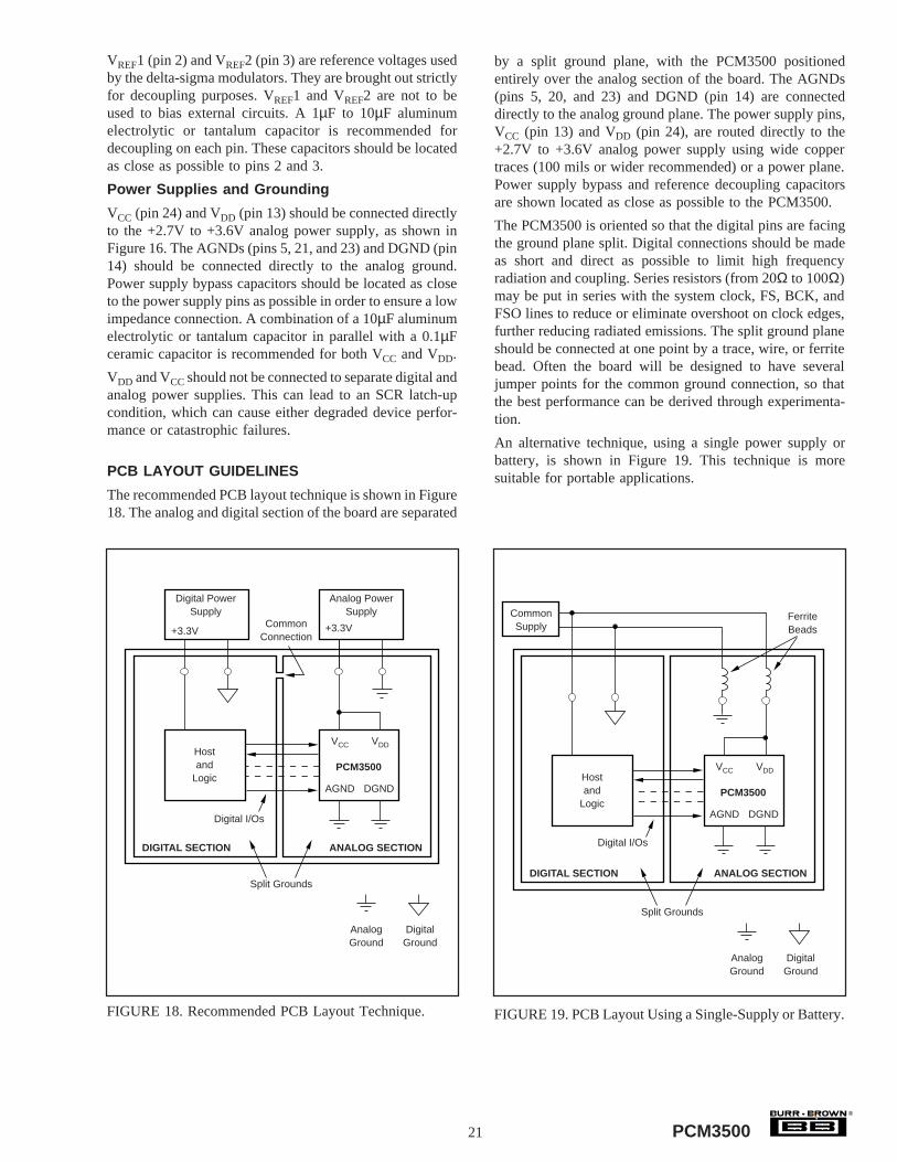
PCB LAYOUT GUIDELINES
The recommended PCB layout technique is shown in Figure18. The analog and digital section of the board are separated
by a split ground plane, with the PCM3500 positionedentirely over the analog section of the board. The AGNDs(pins 5, 20, and 23) and DGND (pin 14) are connecteddirectly to the analog ground plane. The power supply pins,VCC (pin 13) and VDD (pin 24), are routed directly to the+2.7V to +3.6V analog power supply using wide coppertraces (100 mils or wider recommended) or a power plane.Power supply bypass and reference decoupling capacitorsare shown located as close as possible to the PCM3500.
The PCM3500 is oriented so that the digital pins are facingthe ground plane split. Digital connections should be madeas short and direct as possible to limit high frequencyradiation and coupling. Series resistors (from 20Ω to 100Ω)may be put in series with the system clock, FS, BCK, andFSO lines to reduce or eliminate overshoot on clock edges,further reducing radiated emissions. The split ground planeshould be connected at one point by a trace, wire, or ferritebead. Often the board will be designed to have severaljumper points for the common ground connection, so thatthe best performance can be derived through experimenta-tion.
An alternative technique, using a single power supply orbattery, is shown in Figure 19. This technique is moresuitable for portable applications.
FIGURE 18. Recommended PCB Layout Technique. FIGURE 19. PCB Layout Using a Single-Supply or Battery.
PCM3500
VCC VDD
AGND
AnalogGround
DigitalGround
DGND
Digital PowerSupply
Analog PowerSupply
+3.3VCommon
Connection
DIGITAL SECTION ANALOG SECTION
Hostand
Logic
+3.3V
Digital I/Os
Split Grounds
PCM3500
VCC VDD
AGND
Split Grounds
FerriteBeads
AnalogGround
DigitalGround
DGND
DIGITAL SECTION ANALOG SECTION
Hostand
Logic
CommonSupply
Digital I/Os
®
22PCM3500
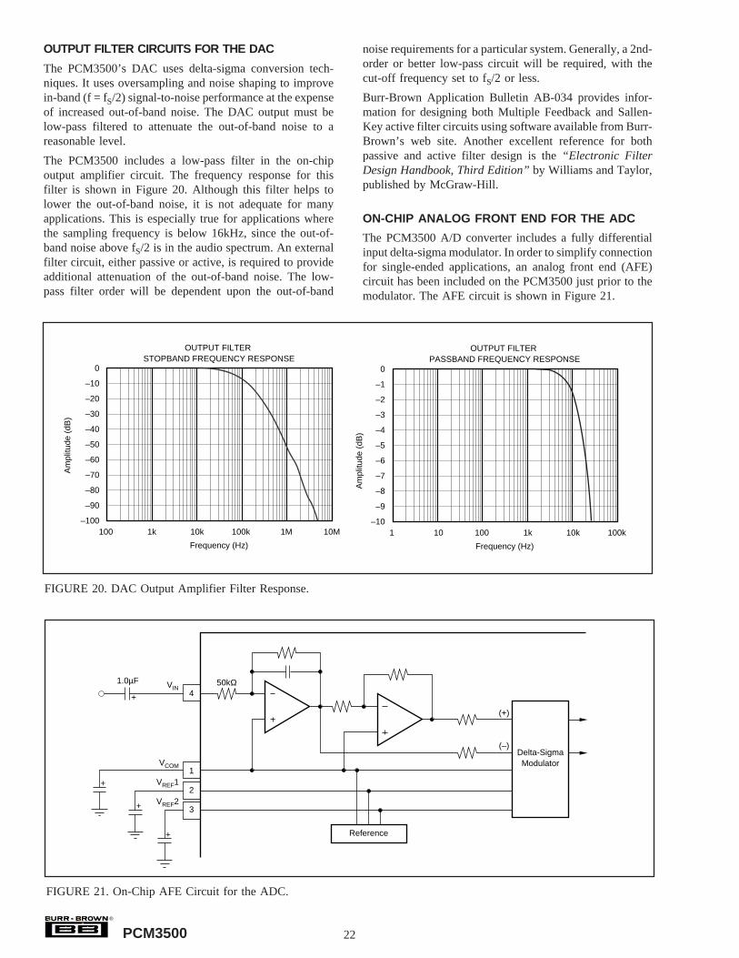
OUTPUT FILTER CIRCUITS FOR THE DAC
The PCM3500’s DAC uses delta-sigma conversion tech-niques. It uses oversampling and noise shaping to improvein-band (f = fS/2) signal-to-noise performance at the expenseof increased out-of-band noise. The DAC output must below-pass filtered to attenuate the out-of-band noise to areasonable level.
The PCM3500 includes a low-pass filter in the on-chipoutput amplifier circuit. The frequency response for thisfilter is shown in Figure 20. Although this filter helps tolower the out-of-band noise, it is not adequate for manyapplications. This is especially true for applications wherethe sampling frequency is below 16kHz, since the out-of-band noise above fS/2 is in the audio spectrum. An externalfilter circuit, either passive or active, is required to provideadditional attenuation of the out-of-band noise. The low-pass filter order will be dependent upon the out-of-band
noise requirements for a particular system. Generally, a 2nd-order or better low-pass circuit will be required, with thecut-off frequency set to fS/2 or less.
Burr-Brown Application Bulletin AB-034 provides infor-mation for designing both Multiple Feedback and Sallen-Key active filter circuits using software available from Burr-Brown’s web site. Another excellent reference for bothpassive and active filter design is the “Electronic FilterDesign Handbook, Third Edition” by Williams and Taylor,published by McGraw-Hill.
ON-CHIP ANALOG FRONT END FOR THE ADC
The PCM3500 A/D converter includes a fully differentialinput delta-sigma modulator. In order to simplify connectionfor single-ended applications, an analog front end (AFE)circuit has been included on the PCM3500 just prior to themodulator. The AFE circuit is shown in Figure 21.
FIGURE 20. DAC Output Amplifier Filter Response.
FIGURE 21. On-Chip AFE Circuit for the ADC.
50kΩVIN4
1
2
3
VCOM
VREF1
VREF2
Delta-SigmaModulator
(+)
(–)
Reference
+
+
1.0µF
+
+
OUTPUT FILTER STOPBAND FREQUENCY RESPONSE
Frequency (Hz)
Am
plitu
de (
dB)
0
–10
–20
–30
–40
–50
–60
–70
–80
–90
–100100 1k 10k 100k 1M 10M
OUTPUT FILTER PASSBAND FREQUENCY RESPONSE
Frequency (Hz)
Am
plitu
de (
dB)
0
–1
–2
–3
–4
–5
–6
–7
–8
–9
–10100101 1k 10k 100k
®
23 PCM3500
ANTI-ALIASING FILTERSTOPBAND CHARACTERISTICS
Frequency (Hz)
Am
plitu
de (
dB)
0
–5
–10
–15
–20
–25
–30
–35
–40
–45
–501k100 10k 100k 1M 10M
ANTI-ALIASING FILTERPASSBAND CHARACTERISTICS
Frequency (Hz)
Am
plitu
de (
dB)
0
–0.1
–0.2
–0.3
–0.4
–0.5
–0.6
–0.7
–0.8
–0.9
–1.01k100101 10k 100k
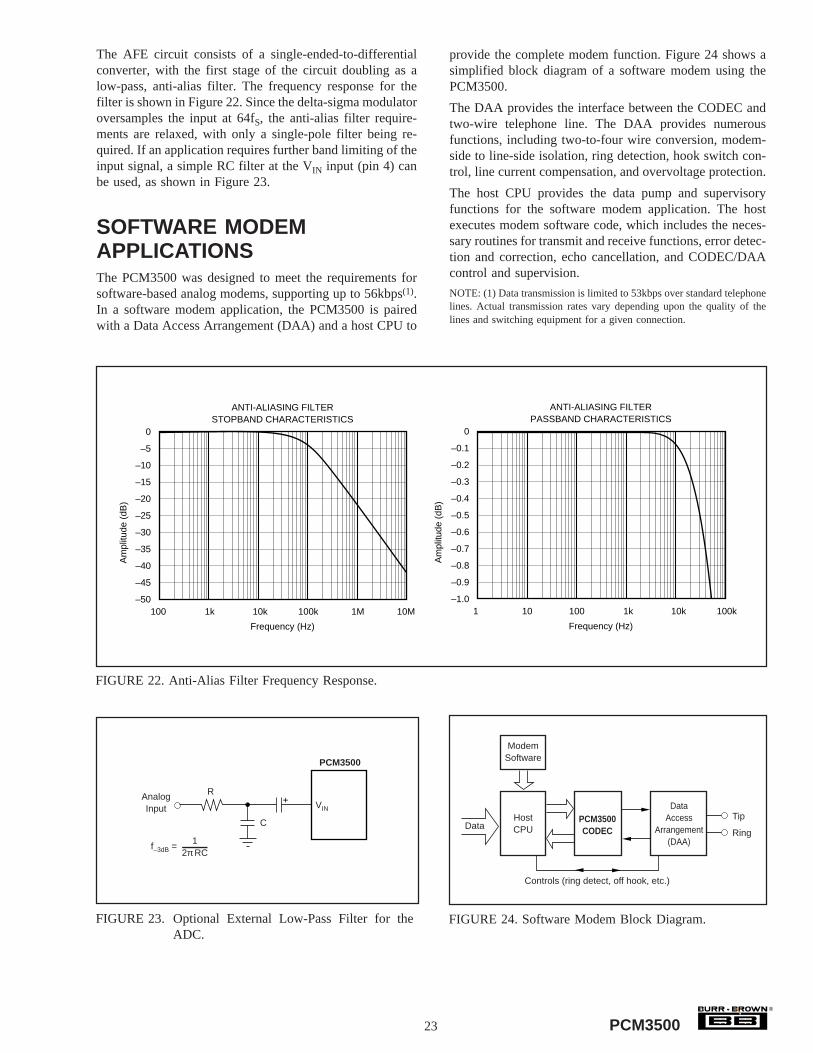
The AFE circuit consists of a single-ended-to-differentialconverter, with the first stage of the circuit doubling as alow-pass, anti-alias filter. The frequency response for thefilter is shown in Figure 22. Since the delta-sigma modulatoroversamples the input at 64fS, the anti-alias filter require-ments are relaxed, with only a single-pole filter being re-quired. If an application requires further band limiting of theinput signal, a simple RC filter at the VIN input (pin 4) canbe used, as shown in Figure 23.
SOFTWARE MODEMAPPLICATIONSThe PCM3500 was designed to meet the requirements forsoftware-based analog modems, supporting up to 56kbps(1).In a software modem application, the PCM3500 is pairedwith a Data Access Arrangement (DAA) and a host CPU to
provide the complete modem function. Figure 24 shows asimplified block diagram of a software modem using thePCM3500.
The DAA provides the interface between the CODEC andtwo-wire telephone line. The DAA provides numerousfunctions, including two-to-four wire conversion, modem-side to line-side isolation, ring detection, hook switch con-trol, line current compensation, and overvoltage protection.
The host CPU provides the data pump and supervisoryfunctions for the software modem application. The hostexecutes modem software code, which includes the neces-sary routines for transmit and receive functions, error detec-tion and correction, echo cancellation, and CODEC/DAAcontrol and supervision.
NOTE: (1) Data transmission is limited to 53kbps over standard telephonelines. Actual transmission rates vary depending upon the quality of thelines and switching equipment for a given connection.
FIGURE 22. Anti-Alias Filter Frequency Response.
FIGURE 23. Optional External Low-Pass Filter for theADC.
FIGURE 24. Software Modem Block Diagram.
+ VIN
PCM3500
AnalogInput
R
C
f–3dB = 12π RC
HostCPU
Controls (ring detect, off hook, etc.)
ModemSoftware
PCM3500CODEC
DataAccess
Arrangement(DAA)
DataTip
Ring
®
24PCM3500
FIG
UR
E 2
5. M
odem
AF
E A
pplic
atio
n C
ircui
t.
HLD
R
LED
CT
HLD
CA
P
HK
P
HK
N
LIN
PW
R
HLF
WV
LR1
LR2
EN
D
CE
N
C1A
VD
D
VS
S
SR
VC
T
SR
VA
N
HIN
VFC
AP
ON
HK
MC
TXA
N
TXC
T
C2
BIA
SE
N
C1B
1 2 3 4 5 6 7 8 9 10 11 12
24 23 22 21 20 19 18 17 16 15 14 13
U1
DL2
07IL
388
8 7 6 5
1 2 3 4
R5
150k
Ω
R6
150k
Ω
C1
15nF
C1
15nF
C3
150n
F
C4
27nF
R2
10M
Ω
D2
Brid
ge
R1
16.5
Ω1%
R9
3.9Ω
R4
356k
Ω
Q2
TN25
40S
OT8
9Q
1M
MB
T652
0S
OT2
3
R3
10M
Ω
C23
0.33
µF25
0V
R20
15kΩ C
151n
F
L 2LI
0805
D12
1R
P310
0BA7
0
RV1
L 1LI
0805
D12
1R
D1
CM
PZD
A18
V
C14
1nF
C8
15nF
C2
150n
FC
947
0pF
C 7 68nF
C 10
470p
FIL
388
U4
U3
1 2 3 4
8 7 6 5
RIN
G
TIP F1
F125
0T
R19
2.4k
Ω1W
, 201
0
R16
6.8M
Ω
R18
12Ω
Q3
FZT6
05
Q4
BC
817-
40
C22
22µF
, 35V
R14
0Ω
+
+
C1B
VR
EF
C2
RX
CT
RX
AN
ON
HK
ML
ON
HK
M
HIN
SR
VA
N
SR
VC
T
TXM
P
VD
D
C1A
LSTA
T
RN
G
OFF
HK
L
OFF
HK
RX
OU
T
AC
RE
F
TXB
IAS
AU
DIN
AU
DO
UT
VS
S
LED
CT
1 2 3 4 5 6 7 8 9 10 11 12
24 23 22 21 20 19 18 17 16 15 14 13
U2
DM
207
VIN
VO
UT
VC
OM
4 22 1
U5
PC
M35
00
R10
10kΩ R
725
.5kΩ R13
27kΩ
C17
4.7n
F
R14
22kΩ
RIN
GD
+3.3
V to
7V
OH
–
R8
121k
Ω
C 5 15nF
C18
1µF
C20
10µF
ISOLATION BARRIER ISOLATION BARRIER
NO
TE
S: A
ll re
sist
ors
are
0.1W
, 5%
, 080
5, u
nles
s ot
herw
ise
note
d.A
ll ca
paci
tors
val
ues
are
10%
, unl
ess
othe
rwis
e no
ted.
O
ptio
nal c
ompo
nent
s.
®
25 PCM3500
Software Modem AFE Application Circuit
Figure 25 shows an applications circuit which utilizes thePCM3500 and the DAA2000 from Infineon Technologies(Siemens) to implement a complete modem AFE. TheDAA2000 provides modem-side (DM207) and line-side(DL207) interfaces, with optical isolation separating thefunctions. The PCM3500 is connected to the modem-side ofthe DAA2000. The PCM3500’s serial interface and hard-ware mode controls are connected to the host CPU.
THEORY OF OPERATIONADC SECTION
The PCM3500 A/D converter consists of two referencecircuits, a mono single-to-differential converter, a fully dif-ferential 5th-order delta-sigma modulator, a decimation fil-ter (including digital high pass), and a serial interface circuit.The block diagram on the front page of this data sheetillustrates the architecture of the ADC section, Figure 21shows the single-to-differential converter, and Figure 26illustrates the architecture of the 5th-order delta-sigma modu-lator and transfer functions.
An internal reference circuit with three external capacitorsprovides all reference voltages which are required by theADC, which defines the full-scale range for the converter.The internal single-to-differential voltage converter savesthe design, space and extra parts needed for external cir-cuitry required by many delta-sigma converters. The internalfull-differential signal processing architecture provides a
wide dynamic range and excellent power supply rejectionperformance. The input signal is sampled at a 64xoversampling rate, eliminating the need for a sample-and-hold circuit, and simplifying anti-alias filtering require-ments. The 5th-order delta-sigma noise shaper consists offive integrators which use a switched-capacitor topology, acomparator, and a feedback loop consisting of a one-bitDAC. The delta-sigma modulator shapes the quantizationnoise, shifting it out of the audio band in the frequencydomain. The high order of the modulator enables it torandomize the modulator outputs, reducing idle tone levels.
The 64fS one-bit data stream from the modulator is con-verted to 1fS, 16-bit data words by the decimation filter,which also acts as a low-pass filter to remove the shapedquantization noise. The DC components can be removed bya high-pass filter function contained within the decimationfilter.
DAC SECTION
The delta-sigma DAC section of PCM3500 is based on a 5-level amplitude quantizer and a 3rd-order noise shaper. Thissection converts the oversampled input data to 5-level delta-sigma format. A block diagram of the 5-level delta-sigmamodulator is shown in Figure 27. This 5-level delta-sigmamodulator has the advantage of stability and clock jittersensitivity over the typical one-bit (2 level) delta-sigmamodulator. The combined oversampling rate of the delta-sigma modulator and the internal 8x interpolation filter is64fS for a 512fS system clock. The theoretical quantizationnoise performance of the 5-level delta-sigma modulator isshown in Figure 28.
++
–+
++
5th SW-CAPIntegrator
4th SW-CAPIntegrator
3rd SW-CAPIntegrator
2nd SW-CAPIntegrator
1st SW-CAPIntegrator
++
++
–++
–
1-BitDAC
H(z)
Qn(z)
Analog InX(z)
Digital OutY(z)
Y(z) = STF(z) • X(z) + NTF(z) • Qn(z)Signal Transfer FunctionNoise Transfer Function
PCM3500E ACTIVE SSOP DB 24 58 Green (RoHS &no Sb/Br)
CU NIPDAU Level-1-260C-UNLIM
PCM3500E/2K ACTIVE SSOP DB 24 2000 Green (RoHS &no Sb/Br)
CU NIPDAU Level-1-260C-UNLIM
PCM3500E/2KG4 ACTIVE SSOP DB 24 2000 Green (RoHS &no Sb/Br)
CU NIPDAU Level-1-260C-UNLIM
PCM3500EG4 ACTIVE SSOP DB 24 58 Green (RoHS &no Sb/Br)
CU NIPDAU Level-1-260C-UNLIM
(1) The marketing status values are defined as follows:ACTIVE: Product device recommended for new designs.LIFEBUY: TI has announced that the device will be discontinued, and a lifetime-buy period is in effect.NRND: Not recommended for new designs. Device is in production to support existing customers, but TI does not recommend using this part ina new design.PREVIEW: Device has been announced but is not in production. Samples may or may not be available.OBSOLETE: TI has discontinued the production of the device.
(2) Eco Plan - The planned eco-friendly classification: Pb-Free (RoHS) or Green (RoHS & no Sb/Br) - please checkhttp://www.ti.com/productcontent for the latest availability information and additional product content details.TBD: The Pb-Free/Green conversion plan has not been defined.Pb-Free (RoHS): TI's terms "Lead-Free" or "Pb-Free" mean semiconductor products that are compatible with the current RoHS requirementsfor all 6 substances, including the requirement that lead not exceed 0.1% by weight in homogeneous materials. Where designed to be solderedat high temperatures, TI Pb-Free products are suitable for use in specified lead-free processes.Green (RoHS & no Sb/Br): TI defines "Green" to mean Pb-Free (RoHS compatible), and free of Bromine (Br) and Antimony (Sb) based flameretardants (Br or Sb do not exceed 0.1% by weight in homogeneous material)
(3) MSL, Peak Temp. -- The Moisture Sensitivity Level rating according to the JEDEC industry standard classifications, and peak soldertemperature.
Important Information and Disclaimer:The information provided on this page represents TI's knowledge and belief as of the date that it isprovided. TI bases its knowledge and belief on information provided by third parties, and makes no representation or warranty as to theaccuracy of such information. Efforts are underway to better integrate information from third parties. TI has taken and continues to takereasonable steps to provide representative and accurate information but may not have conducted destructive testing or chemical analysis onincoming materials and chemicals. TI and TI suppliers consider certain information to be proprietary, and thus CAS numbers and other limitedinformation may not be available for release.
In no event shall TI's liability arising out of such information exceed the total purchase price of the TI part(s) at issue in this document sold by TIto Customer on an annual basis.
IMPORTANT NOTICETexas Instruments Incorporated and its subsidiaries (TI) reserve the right to make corrections, modifications, enhancements, improvements,and other changes to its products and services at any time and to discontinue any product or service without notice. Customers shouldobtain the latest relevant information before placing orders and should verify that such information is current and complete. All products aresold subject to TI’s terms and conditions of sale supplied at the time of order acknowledgment.TI warrants performance of its hardware products to the specifications applicable at the time of sale in accordance with TI’s standardwarranty. Testing and other quality control techniques are used to the extent TI deems necessary to support this warranty. Except wheremandated by government requirements, testing of all parameters of each product is not necessarily performed.TI assumes no liability for applications assistance or customer product design. Customers are responsible for their products andapplications using TI components. To minimize the risks associated with customer products and applications, customers should provideadequate design and operating safeguards.TI does not warrant or represent that any license, either express or implied, is granted under any TI patent right, copyright, mask work right,or other TI intellectual property right relating to any combination, machine, or process in which TI products or services are used. Informationpublished by TI regarding third-party products or services does not constitute a license from TI to use such products or services or awarranty or endorsement thereof. Use of such information may require a license from a third party under the patents or other intellectualproperty of the third party, or a license from TI under the patents or other intellectual property of TI.Reproduction of TI information in TI data books or data sheets is permissible only if reproduction is without alteration and is accompaniedby all associated warranties, conditions, limitations, and notices. Reproduction of this information with alteration is an unfair and deceptivebusiness practice. TI is not responsible or liable for such altered documentation. Information of third parties may be subject to additionalrestrictions.Resale of TI products or services with statements different from or beyond the parameters stated by TI for that product or service voids allexpress and any implied warranties for the associated TI product or service and is an unfair and deceptive business practice. TI is notresponsible or liable for any such statements.TI products are not authorized for use in safety-critical applications (such as life support) where a failure of the TI product would reasonablybe expected to cause severe personal injury or death, unless officers of the parties have executed an agreement specifically governingsuch use. Buyers represent that they have all necessary expertise in the safety and regulatory ramifications of their applications, andacknowledge and agree that they are solely responsible for all legal, regulatory and safety-related requirements concerning their productsand any use of TI products in such safety-critical applications, notwithstanding any applications-related information or support that may beprovided by TI. Further, Buyers must fully indemnify TI and its representatives against any damages arising out of the use of TI products insuch safety-critical applications.TI products are neither designed nor intended for use in military/aerospace applications or environments unless the TI products arespecifically designated by TI as military-grade or "enhanced plastic." Only products designated by TI as military-grade meet militaryspecifications. Buyers acknowledge and agree that any such use of TI products which TI has not designated as military-grade is solely atthe Buyer's risk, and that they are solely responsible for compliance with all legal and regulatory requirements in connection with such use.TI products are neither designed nor intended for use in automotive applications or environments unless the specific TI products aredesignated by TI as compliant with ISO/TS 16949 requirements. Buyers acknowledge and agree that, if they use any non-designatedproducts in automotive applications, TI will not be responsible for any failure to meet such requirements.Following are URLs where you can obtain information on other Texas Instruments products and application solutions:Products ApplicationsAmplifiers amplifier.ti.com Audio www.ti.com/audioData Converters dataconverter.ti.com Automotive www.ti.com/automotiveDSP dsp.ti.com Broadband www.ti.com/broadbandClocks and Timers www.ti.com/clocks Digital Control www.ti.com/digitalcontrolInterface interface.ti.com Medical www.ti.com/medicalLogic logic.ti.com Military www.ti.com/militaryPower Mgmt power.ti.com Optical Networking www.ti.com/opticalnetworkMicrocontrollers microcontroller.ti.com Security www.ti.com/securityRFID www.ti-rfid.com Telephony www.ti.com/telephonyRF/IF and ZigBee® Solutions www.ti.com/lprf Video & Imaging www.ti.com/video