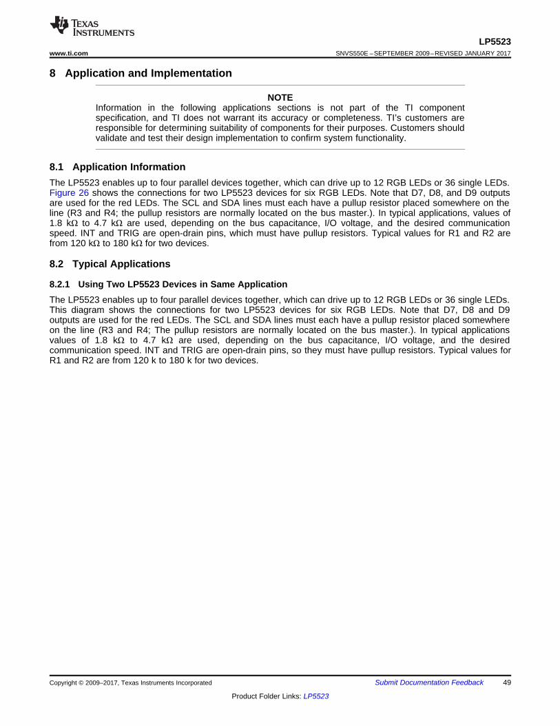
LP5523 D1 D2 D4 D7 VOUT COUT 1 μF C2 0.47 μF ASEL0 ASEL1 GND MCU SCL SDA EN CLK TRIG INT CIN 1 μF VIN = 2.7 V TO 5.5 V VDD C1 0.47 μF C1+ C1- C2+ C2- GPO B G R D3 D8 B G R B G R D6 D5 D9 LP5523 D2 D3 D1 VOUT COUT 1 μF ASEL0 ASEL1 GND MCU SCL SDA EN CLK TRIG INT CIN 1 μF VIN = 2.7 V TO 5.5 V VDD C1+ C1- C2+ C2- GPO D6 D5 D4 D9 D8 D7 RGB LED APPLICATION WLED APPLICATION NOTE: D7, D8 AND D9 POWERED DIRECTLY FROM VIN C2 0.47 μF C1 0.47 μF Product Folder Order Now Technical Documents Tools & Software Support & Community An IMPORTANT NOTICE at the end of this data sheet addresses availability, warranty, changes, use in safety-critical applications, intellectual property matters and other important disclaimers. PRODUCTION DATA. LP5523 SNVS550E – SEPTEMBER 2009 – REVISED JANUARY 2017 LP5523 Nine-Channel RGB- and White-LED Driver With Internal Program Memory and Integrated Charge Pump – DSBGA Package 1 1 Features 1• Three Independent Program Execution Engines, Nine Programmable Outputs with 25.5-mA Full- Scale Current, 8-Bit Current Setting Resolution, and 12-Bit PWM Control Resolution • Adaptive High-Efficiency 1×/1.5× Fractional Charge Pump - Efficiency Up to 94% • LED Drive Efficiency Up to 93% • Charge Pump With Soft Start and Overcurrent and Short-Circuit Protection • Built-in LED Test • 200-nA Typical Standby Current • Automatic Power-Save Mode I VDD = 10 μA (Typical) • Two-Wire I 2 C-Compatible Control Interface • Flexible Instruction Set • Large SRAM Program Memory • Small Application Circuit • Source (High-Side) Drivers • Architecture Supports Color Control 2 Applications • Fun Lights and Indicator Lights • LED Backlighting • Haptic Feedback • Programmable Current Source 3 Description The LP5523 is a 9-channel LED driver designed to produce lighting effects for mobile devices. A high- efficiency charge pump enables LED driving over full Li-Ion battery voltage range. The device is equipped with an internal program memory, which allows operation without processor control. The LP5523 maintains excellent efficiency over a wide operating range by autonomously selecting the best charge-pump gain based on LED forward voltage requirements. The LP5523 is able to automatically enter power-save mode when LED outputs are not active, thus lowering idle current consumption down to 10 μA (typical). The LP5523 has an I 2 C-compatible control interface with four pin selectable addresses. The device has a flexible general purpose output (GPO), which can be used as a digital control pin for other devices. INT pin can be used to notify processor when a lighting sequence has ended (interrupt function). Also, the device has a trigger input interface, which allows synchronization, for example, between multiple LP5523 devices. The device requires only four small, low-cost ceramic capacitors. The LP5523 is available in a tiny 25-pin DSBGA package (0.4-mm pitch). Device Information (1) PART NUMBER PACKAGE BODY SIZE (NOM) LP5523 DSBGA (25) 2.26 mm × 2.26 mm (1) For all available packages, see the orderable addendum at the end of the data sheet. Typical Application
Transcript
LP5523
D1
D2
D4
D7
VOUT
COUT
1 µF
C2
0.47 µF
ASEL0
ASEL1
GND
MCU
SCL
SDA
EN
CLK
TRIG
INT
CIN
1 µF
VIN = 2.7 V TO 5.5 VVDD
C1
0.47 µF
C1+ C1- C2+ C2-
GPO
B
G
R
D3
D8
B
G
R
B
G
R
D6
D5
D9
LP5523
D2
D3
D1
VOUT
COUT
1 µF
ASEL0
ASEL1
GND
MCU
SCL
SDA
EN
CLK
TRIG
INT
CIN
1 µF
VIN = 2.7 V TO 5.5 VVDD
C1+ C1- C2+ C2-
GPOD6
D5
D4
D9
D8
D7
RGB LED APPLICATION
WLED APPLICATION
NOTE: D7, D8 AND D9 POWERED DIRECTLY FROM VIN
C2
0.47 µF
C1
0.47 µF
Product
Folder
Order
Now
Technical
Documents
Tools &
Software
Support &Community
An IMPORTANT NOTICE at the end of this data sheet addresses availability, warranty, changes, use in safety-critical applications,intellectual property matters and other important disclaimers. PRODUCTION DATA.
LP5523SNVS550E –SEPTEMBER 2009–REVISED JANUARY 2017
LP5523 Nine-Channel RGB- and White-LED Driver With InternalProgram Memory and Integrated Charge Pump – DSBGA Package
1
1 Features1• Three Independent Program Execution Engines,
Nine Programmable Outputs with 25.5-mA Full-Scale Current, 8-Bit Current Setting Resolution,and 12-Bit PWM Control Resolution
• Adaptive High-Efficiency 1×/1.5× FractionalCharge Pump - Efficiency Up to 94%
• LED Drive Efficiency Up to 93%• Charge Pump With Soft Start and Overcurrent and
IVDD = 10 µA (Typical)• Two-Wire I2C-Compatible Control Interface• Flexible Instruction Set• Large SRAM Program Memory• Small Application Circuit• Source (High-Side) Drivers• Architecture Supports Color Control
2 Applications• Fun Lights and Indicator Lights• LED Backlighting• Haptic Feedback• Programmable Current Source
3 DescriptionThe LP5523 is a 9-channel LED driver designed toproduce lighting effects for mobile devices. A high-efficiency charge pump enables LED driving over fullLi-Ion battery voltage range. The device is equippedwith an internal program memory, which allowsoperation without processor control.
The LP5523 maintains excellent efficiency over awide operating range by autonomously selecting thebest charge-pump gain based on LED forwardvoltage requirements. The LP5523 is able toautomatically enter power-save mode when LEDoutputs are not active, thus lowering idle currentconsumption down to 10 µA (typical).
The LP5523 has an I2C-compatible control interfacewith four pin selectable addresses. The device has aflexible general purpose output (GPO), which can beused as a digital control pin for other devices. INT pincan be used to notify processor when a lightingsequence has ended (interrupt function). Also, thedevice has a trigger input interface, which allowssynchronization, for example, between multipleLP5523 devices.
The device requires only four small, low-cost ceramiccapacitors. The LP5523 is available in a tiny 25-pinDSBGA package (0.4-mm pitch).
Device Information(1)
PART NUMBER PACKAGE BODY SIZE (NOM)LP5523 DSBGA (25) 2.26 mm × 2.26 mm
(1) For all available packages, see the orderable addendum atthe end of the data sheet.
9 Power Supply Recommendations ...................... 5310 Layout................................................................... 54
10.1 Layout Guidelines ................................................. 5410.2 Layout Example .................................................... 54
11 Device and Documentation Support ................. 5511.1 Device Support .................................................... 5511.2 Receiving Notification of Documentation Updates 5511.3 Community Resources.......................................... 5511.4 Trademarks ........................................................... 5511.5 Electrostatic Discharge Caution............................ 5511.6 Glossary ................................................................ 55
12 Mechanical, Packaging, and OrderableInformation ........................................................... 55
4 Revision HistoryNOTE: Page numbers for previous revisions may differ from page numbers in the current version.
Changes from Revision D (May 2013) to Revision E Page
• Changed title of data sheet for SEO ..................................................................................................................................... 1• Added Device Information and Pin Configuration and Functions sections, ESD Ratings and Thermal Information
tables, Feature Description, Device Functional Modes, Application and Implementation, Power SupplyRecommendations, Layout, Device and Documentation Support, and Mechanical, Packaging, and OrderableInformation sections................................................................................................................................................................ 1
• Changed RθJA value from "87°C/W" to "60.9°C/W" ................................................................................................................ 5• Added values in the Thermal Information table to align with JEDEC standards. .................................................................. 5
Changes from Revision C (April 2013) to Revision D Page
• Changed layout of National Semiconductor data sheet to TI format.................................................................................... 53
(1) A: Analog Pin G: Ground Pin P: Power Pin I: Input Pin I/O: Input/Output Pin O: Output Pin OD: Open Drain Pin
5 Pin Configuration and Functions
YFQ Package25-Pin DSBGA
Top View
YFQ Package25-Pin DSBGABottom View
Pin Functions (1)
PINTYPE DESCRIPTION
NO. NAMEA1 D1 A Current source output 1A2 D2 A Current source output 2A3 VOUT A Charge pump outputA4 C2− A Flying capacitor 2 negative terminalA5 C2+ A Flying capacitor 2 positive terminalB1 D3 A Current source output 3B2 D4 A Current source output 4B3 ASEL1 I Serial interface address select inputB4 C1− A Flying capacitor 1 negative terminalB5 C1+ A Flying capacitor 1 positive terminalC1 D5 A Current source output 5C2 D6 A Current source output 6C3 ASEL0 I Serial interface address select inputC4 EN I EnableC5 VDD P Input power supplyD1 D7 A Current source output 7 - powered from VDD
D2 D8 A Current source output 8 - powered from VDD
D3 INT OD/O Interrupt for microcontroller unit. Leave unconnected if not usedD4 CLK I 32 kHz clock input. Connect to ground if not usedD5 GND G GroundE1 D9 A Current source output 9 - powered from VDD
E2 GPO O General purpose output. Leave unconnected if not usedE3 TRIG I/OD Trigger. Connect to ground if not used.E4 SDA I/OD Serial interface dataE5 SCL I Serial interface clock
(1) Stresses beyond those listed under Absolute Maximum Ratings may cause permanent damage to the device. These are stress ratingsonly, which do not imply functional operation of the device at these or any other conditions beyond those indicated under RecommendedOperating Conditions. Exposure to absolute-maximum-rated conditions for extended periods may affect device reliability.
(2) If Military/Aerospace specified devices are required, contact the TI Sales Office/Distributors for availability and specifications.(3) All voltages are with respect to the potential at the GND pin.
6 Specifications
6.1 Absolute Maximum Ratingsover operating free-air temperature range (unless otherwise noted) (1) (2) (3)
MIN MAX UNITVDD –0.3 6 VVoltage on D1 to D9, C1−, C1+, C2–, C+, VOUT –0.3 VDD + 0.3 V with 6 V maximum VContinuous power dissipation Internally limitedJunction temperature, TJ-MAX 125 °CStorage temperature, Tstg –65 150 °C
(1) JEDEC document JEP155 states that 500-V HBM allows safe manufacturing with a standard ESD control process.(2) JEDEC document JEP157 states that 250-V CDM allows safe manufacturing with a standard ESD control process.
6.2 ESD RatingsVALUE UNIT
V(ESD) Electrostatic discharge
Human-body model (HBM), perANSI/ESDA/JEDEC JS-001 (1)
All pins except D1 to D9 ±2500
VPins D1 to D9 ±8000
Charged-device model (CDM), per JEDECspecification JESD22-C101 (2) All pins ±1000
Machine model All pins 250
(1) All voltages are with respect to the potential at the GND pin.(2) In applications where high power dissipation and/or poor package thermal resistance is present, the maximum ambient temperature may
have to be derated. Maximum ambient temperature (TA-MAX) is dependent on the maximum operating junction temperature (TJ-MAX-OP =125°C), the maximum power dissipation of the device in the application (PD-MAX), and the junction-to ambient thermal resistance of thepart/package in the application (RθJA), as given by the following equation: TA-MAX = TJ-MAX-OP – (RθJA × PD-MAX).
6.3 Recommended Operating Conditionsover operating free-air temperature range (unless otherwise noted) (1) (2)
MIN MAX UNITVDD input voltage 2.7 5.5 VVoltage on logic pins (input or output pins) 0 VDD VRecommended charge pump load current 0 100 mAJunction temperature, TJ –30 125 °CAmbient temperature, TA
(1) For more information about traditional and new thermal metrics, see Semiconductor and IC Package Thermal Metrics.(2) Junction-to-ambient thermal resistance is highly application and board-layout dependent. In applications where high maximum power
dissipation exists, special care must be paid to thermal dissipation issues in board design.
(1) The Electrical Characteristics tables list ensured specifications under Recommended Operating Conditions except as otherwise modifiedor specified by the Electrical Characteristics conditions and/or notes. Typical specifications are estimations only and are not ensured.
(2) All voltages are with respect to the potential at the GND pin.(3) Minimum and maximum limits are ensured by design, test, or statistical analysis.(4) Low-ESR surface-mount ceramic capacitors (MLCCs) used in setting electrical characteristics.
6.5 Electrical CharacteristicsUnless otherwise noted: typical limits are for TA = 25°C; minimum and maximum limits apply over the operating ambienttemperature range (−30°C < TA < +85°C), specifications apply to the Functional Block Diagram with: VDD = 3.6 V, VEN = 1.65V, COUT = 1 µF, CIN = 1 µF, C1–2 = 0.47 µF. (1) (2) (3) (4)
PARAMETER TEST CONDITIONS MIN TYP MAX UNIT
IVDD
Standby supply current
VEN = 0V, CHIP_EN=0 (bit),external 32-kHz clock running or notrunning
0.2 µA
CHIP_EN=0 (bit), external 32 kHzclock not running 1 µA
(1) The Electrical Characteristics tables list ensured specifications under Recommended Operating Conditions except as otherwise modifiedor specified by the Electrical Characteristics conditions and/or notes. Typical specifications are estimations only and are not ensured.
(2) All voltages are with respect to the potential at the GND pin.(3) Minimum and maximum limits are ensured by design, test, or statistical analysis.(4) Turnon time is measured from the moment the charge pump is activated until the VOUT crosses 90% of its target value.
6.6 Charge Pump Electrical CharacteristicsUnless otherwise noted: typical limits are for TA = 25°C; minimum and maximum limits apply over the operating ambienttemperature range (−30°C < TA < +85°C). See (1) (2) (3)
PARAMETER TEST CONDITIONS MIN TYP MAX UNIT
ROUT Charge pump output resistanceGain = 1.5× 3.5
ΩGain = 1× 1
ƒSW Switching frequency 1.25 MHz
IGND Ground currentGain = 1.5× 1.2
mAGain = 1× 0.3
tON VOUT turnon time (4) VDD = 3.6 V, IOUT = 60 mA 100 µs
(1) The Electrical Characteristics tables list ensured specifications under Recommended Operating Conditions except as otherwise modifiedor specified by the Electrical Characteristics conditions and/or notes. Typical specifications are estimations only and are not ensured.
(2) All voltages are with respect to the potential at the GND pin.(3) Minimum and maximum limits are ensured by design, test, or statistical analysis.(4) Output current accuracy is the difference between the actual value of the output current and programmed value of this current. Matching
is the maximum difference from the average. For the constant current outputs on the part (D1 to D9), the following are determined: themaximum output current (MAX), the minimum output current (MIN), and the average output current of all outputs (AVG). Two matchingnumbers are calculated: (MAX – AVG) / AVG and (AVG – MIN) / AVG. The largest number of the two (worst case) is considered thematching figure. Note that some manufacturers have different definitions in use.
(5) Saturation voltage is defined as the voltage when the LED current has dropped 10% from the value measured at VOUT – 1 V.
6.7 LED Driver Electrical CharacteristicsUnless otherwise noted limits apply for TA = 25°C. See (1) (2) (3)
IMAX Maximum source current Outputs D1 to D9 25.5 mA
IOUT Output current accuracy (4) Output current set to 17.5 mA −4% 4%−30°C < TA < +85°C –5% 5%
IMATCH Matching (4) Output current set to 17.5 mA 1% 2.5%ƒLED LED switching frequency 312 HzVSAT Saturation voltage (5) Output current set to 17.5 mA 45 100 mV
(1) The Electrical Characteristics tables list ensured specifications under Recommended Operating Conditions except as otherwise modifiedor specified by the Electrical Characteristics conditions and/or notes. Typical specifications are estimations only and are not ensured.
(2) All voltages are with respect to the potential at the GND pin.(3) Minimum and maximum limits are ensured by design, test, or statistical analysis.(4) Total unadjusted error includes offset, full-scale, and linearity errors.
6.8 LED Test Electrical CharacteristicsUnless otherwise noted limits apply for TA = 25°C. See (1) (2) (3)
PARAMETER TEST CONDITIONS MIN TYP MAX UNITLSB Least significant bit 30 mVEABS Total unadjusted error (4) VIN_TEST = 0 V to VDD < ±3 ±4 LSBtCONV Conversion time 2.7 msVIN_TEST DC voltage range 0 5 V
(1) The Electrical Characteristics tables list ensured specifications under Recommended Operating Conditions except as otherwise modifiedor specified by the Electrical Characteristics conditions and/or notes. Typical specifications are estimations only and are not ensured.
(2) All voltages are with respect to the potential at the GND pin.(3) Minimum and maximum limits are ensured by design, test, or statistical analysis.(4) Low-ESR surface-mount ceramic capacitors (MLCCs) used in setting electrical characteristics.(5) The I2C host must allow at least 500 µs before sending data to the LP5523 after the rising edge of the enable line.
6.9 Logic Interface CharacteristicsUnless otherwise noted: typical limits are for TA = 25°C; minimum and maximum limits apply over the operating ambienttemperature range (−30°C < TA < +85°C).See (1) (2) (3) (4)
PARAMETER TEST CONDITIONS MIN TYP MAX UNITLOGIC INPUT ENVIL Input low level 0.5 VVIH Input high level 1.2 VII Input current −1 1 µAtDELAY Input delay (5) 2 µsLOGIC INPUT SCL, SDA, TRIG, CLK, ASEL0, ASEL1VIL Input low level 0.2 × VEN VVIH Input high level 0.8 × VEN VII Input current −1 1 µALOGIC OUTPUT SDA, TRIG, INTVOL Output low level IOUT = 3 mA (pullup current) 0.3 0.5 VIL Output leakage current VOUT = 2.8 V 1 µALOGIC OUTPUT GPOVOL Output low level IOUT = 3 mA 0.3 0.5 VVOH Output high level IOUT = −2 mA VDD − 0.5 VDD − 0.3IL Output leakage current VOUT = 2.8 V 1 µA
(1) The Electrical Characteristics tables list ensured specifications under Recommended Operating Conditions except as otherwise modifiedor specified by the Electrical Characteristics conditions and/or notes. Typical specifications are estimations only and are not ensured.
(2) All voltages are with respect to the potential at the GND pin.(3) Minimum and maximum limits are ensured by design, test, or statistical analysis.(4) Specification is ensured by design and is not tested in production. VEN = 1.65 V to VDD.(5) The ideal external clock signal for the LP5523 is a 0 V to VEN 25% to 75% duty-cycle square wave. At frequencies above 32.7 kHz,
program execution is faster, and at frequencies below 32.7 kHz program execution is slower.
6.10 Recommended External Clock Source ConditionsUnless otherwise noted limits apply for TA = 25°C. See (1) (2) (3) (4) (5)
MIN NOM MAX UNITLOGIC INPUT CLKƒCLK Clock frequency 32.7 kHztCLKH High time 6 µstCLKL Low time 6 µstr Clock rise time, 10% to 90% 2 µstf Clock fall time, 90% to 10% 2 µs
(1) The Electrical Characteristics tables list ensured specifications under Recommended Operating Conditions except as otherwise modifiedor specified by the Electrical Characteristics conditions and/or notes. Typical specifications are estimations only and are not ensured.
(2) All voltages are with respect to the potential at the GND pin.(3) Minimum and maximum limits are ensured by design, test, or statistical analysis.(4) Minimum and maximum limits are ensured by design, test, or statistical analysis.(5) Specification is ensured by design and is not tested in production. VEN = 1.65 V to VDD.
6.11 Serial Bus Timing Parameters (SDA, SCL)Unless otherwise noted limits apply for TA = 25°C. See (1) (2) (3) (4) (5)
MIN MAX UNITfSCL Clock frequency 400 kHz1 Hold time (repeated) START condition 0.6 µs2 Clock low time 1.3 µs3 Clock high time 600 ns4 Setup TIME FOR A REPEATED START condition 600 ns5 Data hold time 50 ns6 Data setup time 100 ns7 Rise time of SDA and SCL 20+0.1 Cb 300 ns8 Fall time of SDA and SCL 15+0.1 Cb 300 ns9 Set-up time for STOP condition 600 ns10 Bus free time between a STOP and a START condition 1.3 µsCb Capacitive load parameter for each bus line.
Load of one picofarad corresponds to one nanosecond.10 200 ns
Figure 3. Charge Pump 1.5× Efficiency vs Load Current Figure 4. Charge Pump Output Voltage (1.5×) as a Functionof Load Current at Four Input Voltage Levels
6 × 1-mA Load 6 Nichia NSCW100 WLEDs on D1 To D6
Figure 5. Gain Change Hysteresis Loop At Factory Settings
Load = 6 × Nichia NSCW100 WLEDs on D1 To D6 at 100% PWM
Figure 6. Effect of Adaptive Hysteresis on the Width of theHysteresis Loop
17.5-mA CurrentSee note 4 in LED Driver Electrical Characteristics
Figure 7. LED Current Matching Distribution
17.5-mA CurrentSee note 4 in LED Driver Electrical Characteristics
7.1 OverviewThe LP5523 is a fully integrated lighting management unit for producing lighting effects for mobile devices. TheLP5523 includes all necessary power management, high-side current sources, temperature compensation, two-wire control interface and programmable pattern generators. The overall maximum current for each driver is setby an 8-bit register.
The LP5523 controls LED luminance with a pulse width modulation (PWM) scheme with a resolution of 12 bits.Also, the temperature compensation is done by PWM.
7.3.1 ProgrammingThe LP5523 provides flexibility and programmability for dimming and sequencing control. Each LED can becontrolled directly and independently through the serial bus, or LED drivers can be grouped together for pre-programmed flashing patterns.
The LP5523 has three independent program execution engines, so it is possible to form three independentlyprogrammable LED banks. LED drivers can be grouped based on their function so that, for example, the firstbank of drivers can be assigned to the keypad illumination, the second bank to the funlights, and the third groupto the indicator LED(s).
Each bank can contain 1 to 9 LED driver outputs. Instructions for program execution engines are stored in theprogram memory. The total amount of the program memory is 96 instructions, and the user can allocate thememory as required by the engines.
7.3.2 LED Error DetectionThe LP5523 has built-in LED error detection. Error detection does not only detect open and short circuit, butprovides an opportunity to measure the VF of the LEDs. The test event is activated by a serial interface write, andthe results can be read through the serial interface during the next cycle. This feature can also be addressed tomeasure the voltage on VDD, VOUT, and INT pins. Typical example usage includes monitoring battery voltageor using INT pin as a light sensor interface.
7.3.3 Energy EfficiencyWhen charge-pump automatic mode selection is enabled, the LP5523 monitors the voltage over the drivers of D1to D6 so that the device can select the best charge-pump gain and maintain good efficiency over the wholeoperating voltage range. The red LED element of an RGB LED typically has a forward voltage of about 2 V. Forthat reason, the outputs D7, D8, and D9 are internally powered by VDD, since battery voltage is high enough todrive red LEDs over the whole operating voltage range. This allows the driving of three RGB LEDs with goodefficiency because the red LEDs do not load the charge pump. The LP5523 is able to automatically enter power-save mode when LED outputs are not active, thus lowering idle current consumption down to 10 µA (typical).Also, during the down time of the PWM cycle (constant current output status is low), additional power savingscan be achieved when the PWM Powersave feature is enabled.
7.3.4 Temperature CompensationThe luminance of an LED is typically a function of its temperature even though the current flowing through theLED remains constant. Because luminance is temperature dependent, many LED applications require some formof temperature compensation to decrease luminance and color purity variations due to temperature changes. TheLP5523 has a built-in temperature-sensing element, and PWM duty cycle of the LED drivers changes linearly inrelationship to changes in temperature. User can select the slope of the graph (31 slopes) based on the LEDcharacteristics (see Figure 13). This compensation can be done either constantly, or only right after the devicewakes up from power-save mode, to avoid error due to self-heating of the device. Linear compensation isconsidered to be practical and accurate enough for most LED applications.
Compensation is effective over the temperature range −40°C to +90°C.
7.3.5 Charge Pump Operational Description
7.3.5.1 OverviewThe LP5523 includes a pre-regulated switched-capacitor charge pump with a programmable voltagemultiplication of 1× and 1.5×. In 1.5× mode, by combining the principles of a switched-capacitor charge pumpand a linear regulator, a regulated 4.5-V output is generated from the Li-Ion input voltage range. A two-phasenon-overlapping clock generated internally controls the operation of the charge pump. During the charge phase,both flying capacitors (C1 and C2) are charged from input voltage. In the pump phase that follows, the flyingcapacitors are discharged to output. A traditional switched-capacitor charge pump operating in this manner usesswitches with very low on-resistance, ideally 0 Ω, to generate an output voltage that is 1.5× the input voltage.The LP5523 regulates the output voltage by controlling the resistance of the input-connected pass-transistorswitches in the charge pump.
7.3.5.2 Output ResistanceAt lower input voltages, the charge pump output voltage may degrade due to effective output resistance (ROUT) ofthe charge pump. The expected voltage drop can be calculated by using a simple model for the charge pumpshown in Figure 14.
Figure 14. Charge Pump Output Resistance Model
The model shows a linear pre-regulation block (REG), a voltage multiplier (1.5×), and an output resistance(ROUT). Output resistance models the output voltage drop that is inherent to switched capacitor converters. Theoutput resistance is 3.5 Ω (typical), and it is a function of switching frequency, input voltage, capacitance value ofthe flying capacitor, internal resistances of the switches, and ESR of the flying capacitors. When the outputvoltage is in regulation, the regulator in the model controls the voltage V’ to keep the output voltage equal to 4.5V (typical).
Feature Description (continued)With increased output current, the voltage drop across ROUT increases. To prevent drop in output voltage, thevoltage drop across the regulator is reduced, V’ increases, and VOUT remains at 4.5 V. When the output currentincreases to the point that there is zero voltage drop across the regulator, V’ equals the input voltage, and theoutput voltage is on the edge of regulation. Additional output current causes the output voltage to fall out ofregulation, so that the operation is similar to a basic open-loop 1.5× charge pump. In this mode, output currentresults in output voltage drop proportional to the output resistance of the charge pump. The out-of-regulationoutput voltage can be approximated by: VOUT = 1.5 × VIN – IOUT × ROUT.
7.3.5.3 Controlling The Charge PumpThe charge pump is controlled with two CP_MODE bits in MISC register (address 36H). When both of the bitsare low, the charge pump is disabled, and output voltage is pulled down with an internal 300 kΩ (typ.) resistor.The charge pump can be forced to bypass mode, so the battery voltage is connected directly to the currentsources; in 1.5×mode output voltage is boosted to 4.5 V. In automatic mode, charge-pump operation mode isdetermined by saturation of constant current drivers, as described in LED Forward Voltage Monitoring.
7.3.5.4 LED Forward Voltage MonitoringWhen the charge-pump automatic mode selection is enabled, voltages over LED drivers D1 to D6 are monitored.(Note: Power input for current source outputs D7, D8 and D9 are internally connected to the VDD pin.) If the D1to D6 drivers do not have enough headroom, charge-pump gain is set to 1.5×. Driver saturation monitor does nothave a fixed voltage limit, since saturation voltage is a function of temperature and current. Charge pump gain isset to 1×, when battery voltage is high enough to supply all LEDs.
In automatic gain change mode, the charge pump is switched to bypass mode (1×), when LEDs are inactive forover 50 ms.
7.3.5.5 Gain Change HysteresisCharge-pump-gain control utilizes digital filtering to prevent supply voltage disturbances (for example, thetransient voltage on the power supply during the GSM burst) from triggering unnecessary gain changes.Hysteresis is provided to prevent periodic gain changes (which could occur due to LED driver) and charge-pumpvoltage drop in 1× mode. The hysteresis of the gain change is user-configurable; default setting is factory-programmable. Flexible configuration ensures that hysteresis can be minimized or set to desired level in eachapplication.
LED forward voltage monitoring and gain control block diagram is shown in Figure 15.
Figure 15. Forward Voltage Monitoring and Gain Control Block
Feature Description (continued)7.3.6 LED Driver Operational Description
7.3.6.1 OverviewThe LP5523 LED drivers are constant-current sources. Output current can be programmed by control registersup to 25.5 mA. The overall maximum current is set by 8-bit output current control registers with 100-μA step size.Each of the 9 LED drivers has a separate output-current control register.
The LED luminance pattern (dimming) is controlled with PWM (pulse width modulation) technique, which hasinternal resolution of 12 bits (8-bit control can be seen by user). PWM frequency is 312 Hz. See Figure 16.
Figure 16. LED Pattern and Current Control Principle
LED dimming is controlled according to a logarithmic or linear scale, see Figure 17. A logarithmic or linearscheme can be set for both the program execution engine control and direct PWM control. Note: if thetemperature compensation is active, the maximum PWM duty cycle is limited to 50% at 25°C. This is required toallow enough headroom for temperature compensation over the whole temperature range −40°C to +90°C.
Figure 17. Logarithmic vs Linear Dimming
7.3.6.2 Powering LEDsThe LP5523 is very suitable for white LED and general purpose applications, and it is particularly well suited touse with RGB LEDs. The device architecture is optimized for use with three RGB LEDs. Typically, the red LEDshave forward voltages below 2 volts, thus red LEDs can be powered directly from VDD. In the LP5523 device theD7, D8, and D9 drivers are powered from the battery voltage (VDD), not from the charge-pump output. D1 to D6drivers are internally connected to the charge-pump output, and these outputs can be used for driving green andblue (VF = 2.7 V to 3.7 V typical) or white LEDs. Of course, D7, D8, and D9 outputs can be used for green, blueor white LEDs if the VDD voltage is high enough.
An RGB LED configuration example is given in Typical Applications.
Feature Description (continued)7.3.6.3 Controlling The High-Side LED Drivers1. Direct PWM Control: All LP5523 LED drivers, D1 to D9, can be controlled independently through the two-wire
serial I2C-compatible interface. For each high-side driver there is a PWM control register. Direct PWM controlis active by default.
2. Controlling by Program Execution Engines: Engine control is used when the user wants to createprogrammed sequences. The program execution engine has a higher priority than direct control registers.Therefore, if the user has set the PWM register to a certain value, it is automatically overridden when theprogram execution engine controls the driver. LED control and program execution engine operation isdescribed in Control Register Details.
3. Master Fader Control: In addition to LED-by-LED PWM register control, the LP5523 is equipped with so-called master fader control, which allows the user to fade in or fade out multiple LEDs by writing to only oneregister. This is a useful function to minimize serial-bus traffic between the MCU and the LP5523. TheLP5523 has three master fader registers, so it is possible to form three master fader groups.
7.4.1 Modes Of OperationRESET In the RESET mode all the internal registers are reset to the default values. Reset is always
entered if Reset Register (3DH) is written FFH or internal Power-On Reset is active. Power-OnReset (POR) activates during the chip startup or when the supply voltage VDD fall below 1.5V (typ.).Once VDD rises above 1.5V (typ.), POR deactivates, and the device continues to the STANDBYmode. CHIP_EN control bit is low after POR by default.
STANDBY: The STANDBY mode is entered if the register bit CHIP_EN or EN pin is LOW, and Reset is notactive. This is the low-power consumption mode, when all circuit functions are disabled. Mostregisters can be written in this mode if EN pin is risen to high so that control bits are effective rightafter the startup (see Control Register Details).
STARTUP: When CHIP_EN bit is written high and EN pin is high, the INTERNAL STARTUP SEQUENCEpowers up all the needed internal blocks (VREF, bias, oscillator etc.). Startup delay is 500 μs. If thechip temperature rises too high, the Thermal shutdown (TSD) disables the chip operation, and thechip waits in STARTUP mode until no thermal shutdown event is present.
NORMAL: During NORMAL mode the user controls the chip using the Control Registers.
POWER SAVE: In POWER-SAVE mode analog blocks are disabled to minimize power consumption. SeeAutomatic Power-Save Mode for further information.
Device Functional Modes (continued)7.4.1.1 Automatic Power-Save ModeAutomatic power-save mode is enabled when POWERSAVE_EN bit in register address 36H is 1. Almost allanalog blocks are powered down in power-save if an external clock signal is used. Only the charge-pumpprotection circuits remain active. However, if the internal clock has been selected, only charge pump and LEDdrivers are disabled during the power save; the digital part of the LED controller needs to stay active. In bothcases the charge pump enters the weak 1× mode. In this mode the charge pump utilizes a passive currentlimited keep-alive switch, which keeps the output voltage at the battery level. During the program executionLP5523 can enter power save if there is no PWM activity in any of the LED driver outputs. To prevent shortpower-save sequences during program execution, LP5523 has an instruction look-ahead filter. During programexecution engine 1, engine 2 and engine 3 instructions are constantly analyzed, and if there are time intervals ofmore than 50 ms in length with no PWM activity on LED driver outputs, the device enters power save. In power-save mode program execution continues uninterrupted. When an instruction that requires PWM activity isexecuted, a fast internal-startup sequence is started automatically.
7.4.1.2 PWM Power-Save ModePWM cycle power-save mode is enabled when register 36 bit [2] PWM_PS_EN is set to 1. In PWM power-savemode analog blocks are powered down during the "down time" of the PWM cycle. Which blocks are powereddown depends whether the external or internal clock is used. While the Automatic Power-Save Mode (seeabove) saves energy when there is no PWM activity at all, the PWM power-save mode saves energy duringPWM cycles. Like the automatic power-save mode, PWM power-save mode also works during programexecution. Figure 18 shows the principle of the PWM power-save technique. An LED on D9 output is driven at50% PWM, 5-mA current (top waveform). After PWM Power-save enable, the LED-current remains the same, butthe LP5523 input current drops down to an approximately 50-µA level when the LED is OFF, or to anapproximately 200-µA level when the charge-pump-powered output(s) are used.
7.5.1 I2C-Compatible Control InterfaceThe I2C-compatible synchronous serial interface provides access to the programmable functions and registers onthe device. This protocol uses a two-wire interface for bidirectional communications between the devicesconnected to the bus. The two interface lines are the Serial Data Line (SDA), and the Serial Clock Line (SCL).Every device on the bus is assigned a unique address and acts as either a Master or a Slave depending onwhether it generates or receives the serial clock SCL. The SCL and SDA lines should each have a pullup resistorplaced somewhere on the line and remain HIGH even when the bus is idle. Note: CLK pin is not used for serialbus data transfer.
7.5.1.1 Data ValidityThe data on SDA line must be stable during the HIGH period of the clock signal (SCL). In other words, state ofthe data line can only be changed when clock signal is LOW.
Figure 19. Data Validity Diagram
7.5.1.2 Start and Stop ConditionsSTART and STOP conditions classify the beginning and the end of the data transfer session. A START conditionis defined as the SDA signal transitioning from HIGH to LOW while SCL line is HIGH. A STOP condition isdefined as the SDA transitioning from LOW to HIGH while SCL is HIGH. The bus master always generatesSTART and STOP conditions. The bus is considered to be busy after a START condition and free after a STOPcondition. During data transmission, the bus master can generate repeated START conditions. First START andrepeated START conditions are equivalent, function-wise.
7.5.1.3 Transferring DataEvery byte put on the SDA line must be eight bits long, with the most significant bit (MSB) being transferred first.Each byte of data has to be followed by an acknowledge bit. The acknowledge related clock pulse is generatedby the master. The master releases the SDA line (HIGH) during the acknowledge clock pulse. The LP5523 pullsdown the SDA line during the 9th clock pulse, signifying an acknowledge. The LP5523 generates anacknowledge after each byte has been received.
There is one exception to the “acknowledge after every byte” rule. When the master is the receiver, it mustindicate to the transmitter an end of data by not acknowledging (“negative acknowledge”) the last byte clockedout of the slave. This “negative acknowledge” still includes the acknowledge clock pulse (generated by themaster), but the SDA line is not pulled down.
After the START condition, the bus master sends a chip address. This address is seven bits long followed by aneighth bit which is a data direction bit (READ or WRITE). The LP5523 address is defined with ASEL0 and ASEL1pins, and it is 32h when ASEL1 and ASEL0 are connected to GND. For the eighth bit, a “0” indicates a WRITEand a “1” indicates a READ. The second byte selects the register to which the data is written. The third bytecontains data to write to the selected register.
(HEX) WRITE/READGND GND 32 64/65GND VEN 33 66/67VEN GND 34 68/69VEN VEN 35 6A/6B
Figure 20. LP5523 Chip Address
This data pattern writes temperature information to the TEMPERATURE WRITE register (40h).
Figure 21. Write Cycle (W = Write; SDA = 0), Id = Chip Address = 32h for LP5523
This data pattern reads temperature information from the TEMPERATURE READ register (3Fh). When a READfunction is to be accomplished, a WRITE function must precede the READ function.
Figure 22. Read Cycle (R = Read; SDA = 1), Id = Chip Address = 32h for LP5523
7.5.1.4.1 Control Register Write Cycle• Master device generates start condition.• Master device sends slave address (7 bits) and the data direction bit (r/w = 0).• Slave device sends acknowledge signal if the slave address is correct• Master sends control register address (8 bits).• Slave sends acknowledge signal.• Master sends data byte to be written to the addressed register.• Slave sends acknowledge signal.• If master sends further data bytes, the slave’s control register address is incremented by one after
acknowledge signal. In order to reduce program load time, the LP5523 supports address auto incrementation.Register address is incremented after each 8 data bits. For example, the whole program memory page canbe written in one serial bus write sequence. Note: serial bus address auto increment is not supported forregister addresses from 16 to 1E.
• Write cycle ends when the master creates stop condition.
7.5.1.4.2 Control Register Read Cycle• Master device generates a start condition.• Master device sends slave address (7 bits) and the data direction bit (r/w = 0).• Slave device sends acknowledge signal if the slave address is correct• Master sends control register address (8 bits).• Slave sends acknowledge signal.• Master device generates repeated start condition.• Master sends the slave address (7 bits) and the data direction bit (r/w = 1).• Slave sends acknowledge signal if the slave address is correct.• Slave sends data byte from addressed register.• If the master device sends an acknowledge signal, the control register address is incremented by one. Slave
device sends data byte from addressed register.• Read cycle ends when the master does not generate acknowledge signal after data byte and generates stop
condition
7.5.1.4.3 Auto-Increment Feature
The auto-increment feature allows writing several consecutive registers within one transmission. Every time an 8-bit word is sent to the LP5523, the internal address index counter is incremented by one, and the next register iswritten. Example below (Table 2) shows writing sequence to two consecutive registers. Auto-increment feature isenabled by writing EN_AUTO_INCR bit high in the MISC register (addr 36h). Note: serial bus address autoincrement is not supported for register addresses from 16 to 1E.
7.6.1 Register SetThe LP5523 is controlled by a set of registers through the two-wire serial interface port. Some register bits arereserved for future use. Table 3 lists device registers, their addresses and their abbreviations. A more detaileddescription is given in Control Register Details.
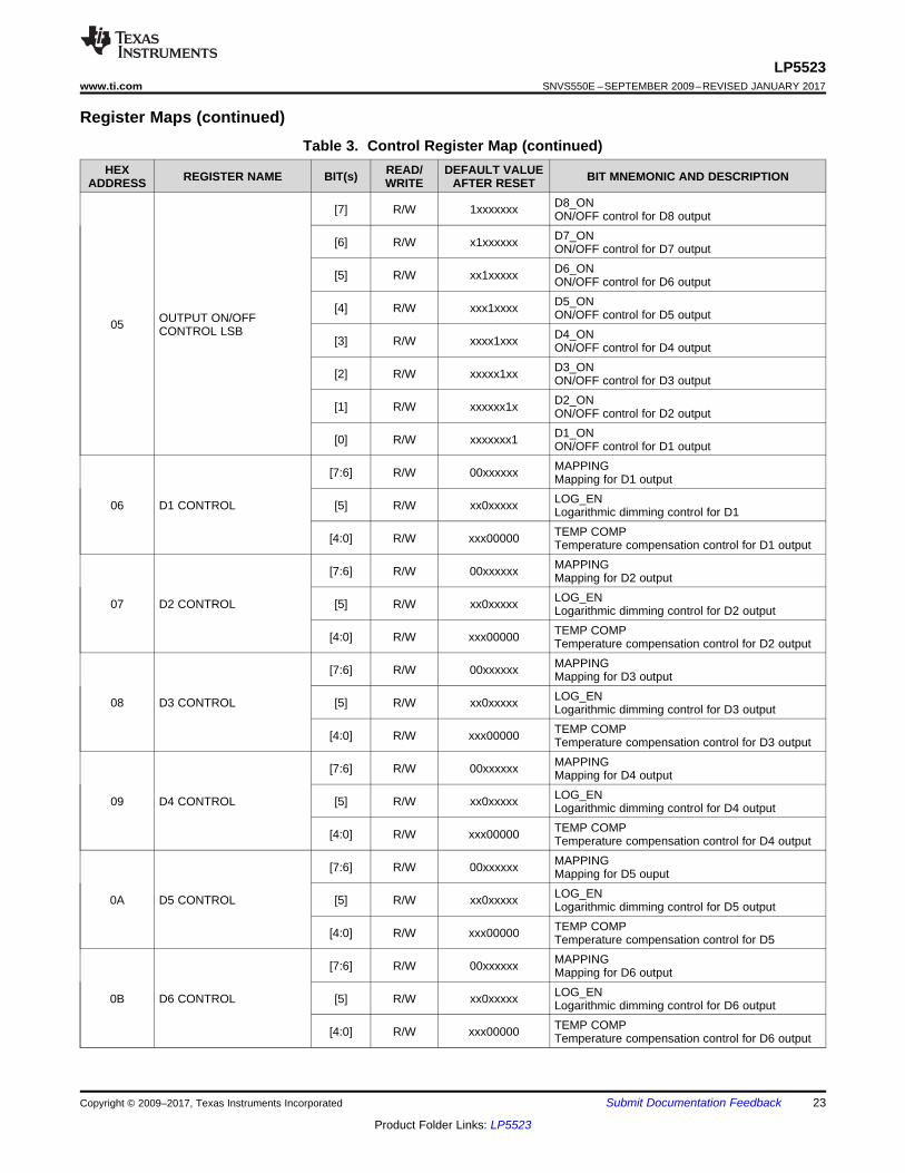
Table 3. Control Register MapHEX
ADDRESS REGISTER NAME BIT(s) READ/WRITE
DEFAULT VALUEAFTER RESET BIT MNEMONIC AND DESCRIPTION
00 ENABLE / ENGINECNTRL1
[6] R/W x0xxxxxxCHIP_EN0 = LP5523 not enabled1 = LP5523 enabled
[5:4] R/W xx00xxxx ENGINE1_EXECEngine 1 program execution control
[3:2] R/W xxxx00xx ENGINE2_EXECEngine 2 program execution control
[1:0] R/W xxxxxx00 ENGINE3_EXECEngine 3 program execution control
01 ENGINE CNTRL2
[5:4] R/W xx00xxxx ENGINE1_MODEENGINE 1 mode control
[3:2] R/W xxxx00xx ENGINE2_MODEENGINE 2 mode control
[1:0] R/W xxxxxx00 ENGINE3_MODEENGINE 3 mode control
02OUTPUTDIRECT/RATIOMETRICMSB
[0] R/W xxxxxxx0 D9_RATIO_ENEnables ratiometric dimming for D9 output.
03OUTPUTDIRECT/RATIOMETRICLSB
[7] R/W 0xxxxxxx D8_RATIO_ENEnables ratiometric dimming for D8 output.
[6] R/W x0xxxxxx D7_RATIO_ENEnables ratiometric dimming for D7 output.
[5] R/W xx0xxxxx D6_RATIO_ENEnables ratiometric dimming for D6 output.
[4] R/W xxx0xxxx D5_RATIO_ENEnables ratiometric dimming for D5 output.
[3] R/W xxxx0xxx D4_RATIO_ENEnables ratiometric dimming for D4 output.
[2] R/W xxxxx0xx D3_RATIO_ENEnables ratiometric dimming for D3 output.
[1] R/W xxxxxx0x D2_RATIO_ENEnables ratiometric dimming for D2 output.
[0] R/W xxxxxxx0 D1_RATIO_ENEnables ratiometric dimming for D1 output.
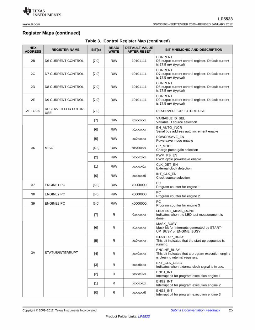
Register Maps (continued)Table 3. Control Register Map (continued)
HEXADDRESS REGISTER NAME BIT(s) READ/
WRITEDEFAULT VALUE
AFTER RESET BIT MNEMONIC AND DESCRIPTION
50 PROGRAM MEMORY00H/10H/20H/30H/40H/50H
[15:8] R/W 00000000
CMDEvery Instruction is 16-bit width.The LP5523 can store 96 instructions. Eachinstruction consists of 16 bits. Because oneregister has only 8 bits, one instruction requirestwo register addresses. In order to reduceprogram load time the LP5523 supports addressauto-incrementation. Register address isincremented after each 8 data bits. Thus thewhole program memory page can be written inone serial bus write sequence.
[2] R/W xxxxx0xx FORCE_1xActivates 1.5× to 1× timer.
7.6.2 Control Register Details00 ENABLE/ ENGINE CONTROL1• 00 - Bit [6] CHIP_EN
– 1 = internal start-up sequence powers up all the needed internal blocks and the device enters normalmode.
– 0 = standby mode is entered. Control registers can still be written or read, excluding bits[5:0] in reg 00(this register), registers 16h to 1E (LED PWM registers) and 37h to 39h (program counters).
• 00 — Bits [5:4] ENGINE1_EXEC– Engine 1 program execution control. Execution register bits define how the program is executed. Program
start address can be programmed to Program Counter (PC) register 37H.– 00 = hold: Hold causes the execution engine to finish the current instruction and then stop. Program
counter (PC) can be read or written only in this mode.– 01 = step: Execute the instruction at the location pointed by the PC, increment the PC by one and then
reset ENG1_EXEC bits to 00 (i.e. enter hold).– 10 = free run: Start program execution from the location pointed by the PC.– 11 = execute once: Execute the instruction pointed by the current PC value and reset ENG1_EXEC to 00
(that is, enter hold). The difference between step and execute once is that execute once does notincrement the PC.
• 00 — Bits [3:2] ENGINE2_EXEC– Engine 2 program execution control. Equivalent to above definition of control bits. Program start address
can be programmed to PC register 38H.• 00 — Bits [1:0] ENGINE3_EXEC
– Engine 3 program execution control. Equivalent to engine 1 control bits. Program start address can beprogrammed to PC register 39H.
01 ENGINE CONTROL2• Operation modes are defined in this register.
– Disabled: Engines can be configured to disabled mode each one separately.– Load program: Writing to program memory is allowed only when the engine is in load program operation
mode and engine busy bit (reg 3A) is not set. Serial bus master should check the busy bit before writing toprogram memory or allow at least 1ms delay after entering to load mode before memory write, to ensureinitalization. All the three engines are in hold while one or more engines are in load program mode. PWMvalues are frozen, also. Program execution continues when all the engines are out of load program mode.Load program mode resets the program counter of the respective engine. Load program mode can beentered from the disabled mode only. Entering load program mode from the run program mode is notallowed.
– Run Program:Run program mode executes the instructions stored in the program memory. Executionregister (ENG1_EXEC etc.) bits define how the program is executed (hold, step, free run or executeonce). Program start address can be programmed to the PC register. The PC is reset to zero when thePC’s upper limit value is reached.
– Halt: Instruction execution aborts immediately, and engine operation halts.– 01 — Bit [5:4] ENGINE1_MODE– 00 = disabled.– 01 = load program to SRAM, reset engine 1 PC.– 10 = run program as defined by ENGINE1_EXEC bits.– 11 = halts the engine.– 01 — Bits [3:2] ENGINE2_MODE– 00 = disabled.– 01 = load program to SRAM, reset engine 2 PC.– 10 = run program as defined by ENGINE2_EXEC bits.– 11 = halts the engine.– 01 — Bits [3:2] ENGINE3_MODE– 00 = disabled.– 01 = load program to SRAM, reset engine 3 PC.– 10 = run program as defined by ENGINE3_EXEC bits.– 11 = halts the engine.
02 OUTPUT DIRECT/RATIOMETRIC MSBA particular feature of the LP5523 is the ratiometric up/down dimming of the RGB LEDs. In other words, the LEDdriver PWM output varies in a ratiometric manner. By a ratiometric approach the emitted color of an RGB LEDremains the same regardless of the initial magnitudes of the R/G/B PWM outputs. For example, if the PWMoutput of the red LED output is doubled, the output of green LED is doubled also.• 02 — Bit [0] D9_RATIO_EN
– 1 = enables ratiometric dimming for D9 output.– 0 = disables ratiometric dimming for D9 output.
03 OUTPUT DIRECT/RATIOMETRIC LSB• 03 — Bit [7] D8_RATIO_EN
– 1 = enables ratiometric dimming for D8 output.– 0 = disables ratiometric dimming for D8 output.–
• 03 — Bit [0] D1_RATIO_EN to Bit [6] D7_RATIO_EN– The options for D1 output to D7 output are the same as previous: see 03 — Bit [7].–
– 1 = D8 output ON.– 0 = D8 output OFF.– Note: Engine mapping over rides this control.
• 05 — Bit [0] D1_ON to Bit [6] D7_ON– The options for D1 output to D7 output are the same as above — see the “05 — Bit [7]” section.
06 D1 CONTROLThis is the register used to assign the D1 output to the MASTER FADER group 1, 2, or 3, or none of them. Also,this register sets the correction factor for the D1 output temperature compensation and selects between linearand logarithmic PWM brightness adjustment. By using logarithmic PWM-scale the visual effect looks like linear.When the logarithmic adjustment is enabled, the device handles internal PWM values with 12-bit resolution. Thisallows very fine-grained PWM control at low PWM duty cycles.• 06 — Bit [7:6] MAPPING
– 00 = no master fader set, clears master fader set for D1. Default setting.– 01 = MASTER FADER1 controls the D1 output.– 10 = MASTER FADER2 controls the D1 output.– 11 = MASTER FADER3 controls the D1 output.– The duty cycle on D1 output is the D1 PWM register value (address 16H) multiplied with the value in the
MASTER FADER register.• 06 — Bit [5] LOG_EN
–– 0 = linear adjustment.– 1 = logarithmic adjustment.– This bit is effective for both the program execution engine control and direct PWM control.
• 06 — Bit [4:0] TEMP_COMP– The reference temperature is 25°C (that is, the temperature at which the compensation has no effect) and
the correction factor (slope) can be set in 0.1% 1/°C steps to any value between −1.5% 1/°C and +1.5%1/°C, with a default to 0.0% 1/°C.
TEMP_COMP BITS CORRECTION FACTOR (%)00000 Not activated - default setting after reset.11111 −1.5 1/°C11110 −1.4 1/°C
The PWM duty cycle at temperature T (in centigrade) can be obtained as follows: PWMF = [PWMS – (25 – T) ×correction factor × PWMS] / 2, where PWMF is the final duty cycle at temperature T, PWMS is the set PWM dutycycle (PWM duty cycle is set in registers 16H to 1EH) and the value of the correction factor is obtained from thetable above.
For example, if the set PWM duty cycle in register 16H is 90%, temperature T is −10°C, and the chosencorrection factor is 1.5% 1/°C, the final duty-cycle PWMF for D1 output is [90% – (25°C − (−10°C)) × 1.5% 1/°C ×90%] / 2 = [90% – 35 × 0.015 × 90%] / 2 = 21.4%. Default setting 00000 means that the temperaturecompensation is non-active and the PWM output (0 to 100%) is set solely by PWM registers D1 PWM to D9PWM.
07 D2 CONTROL to 0E D9 CONTROL• The control registers and control bits for D2 output to D9 output are similar to that given to D1, see previous
06 – Bit [5] and 06 – Bits [4:0].
16 D1 PWM• This is the PWM duty cycle control for D1 output. D1 PWM register is effective during direct control operation;
direct PWM control is active after power up by default. Note: serial bus address auto increment is notsupported for register addresses from 16 to 1E.– 16 — Bits [7:0] PWM
– These bits set the D1 output PWM as shown in Figure 23. Note: if the temperature compensation isactive, the maximum PWM duty cycle is 50% at 25°C. This is required to allow enough headroom fortemperature compensation over the temperature range −40°C to +90°C.
Figure 23. Direct PWM Control Bits vs PWM Duty Cycle
17 D2 PWM to 1E D9 PWM• PWM duty cycle control for outputs D2 to D9. The control registers and control bits for D2 output to D9 output
are similar to that given to D1.
26 D1 CURRENT CONTROL• D1 LED driver output current control register. The resolution is 8-bits and step size is 100 μA.
CURRENT bits OUTPUT CURRENT (TYPICAL)00000000 0.0 mA00000001 0.1 mA00000010 0.2 mA
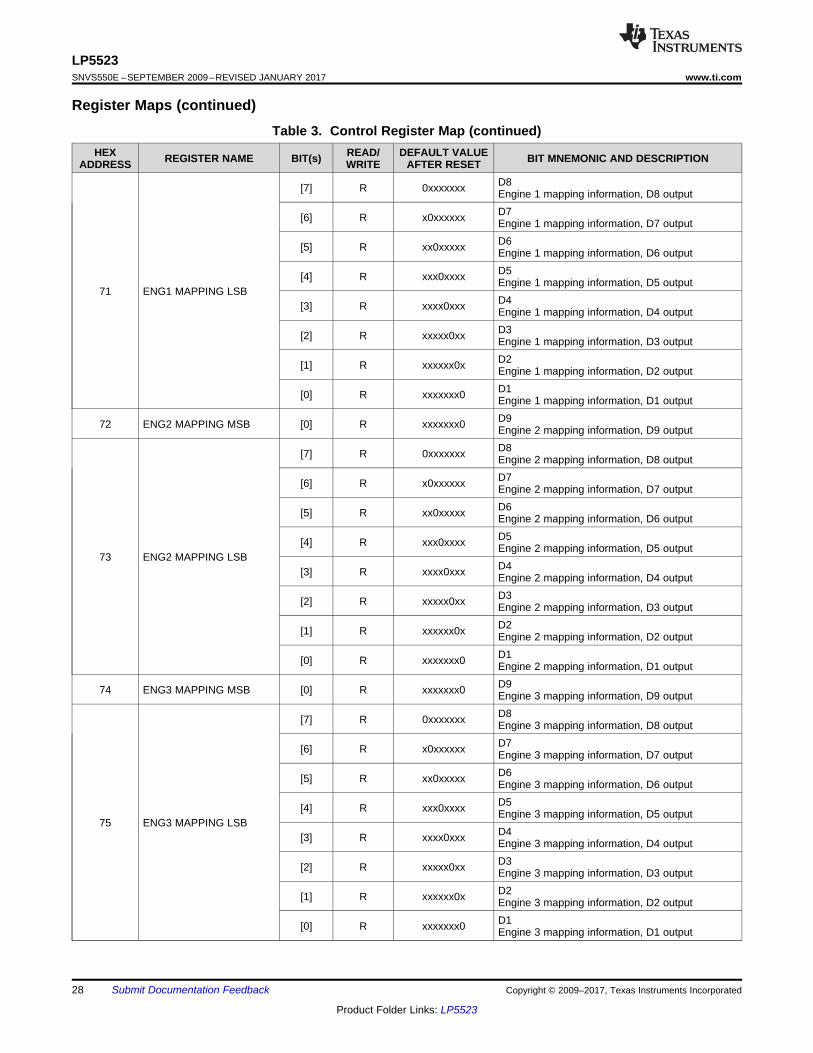
27 D2 CURRENT CONTROL to 2E D9 CURRENT CONTROL• The control registers and control bits for D2 output up to D9 output are similar to that given to D1 output.
36 MISC• This register contains miscellaneous control bits.
– 36 — Bit [7] VARIABLE_D_SEL– Variable D source selection– 1 = variable D source is the LED test ADC output (LED TEST ADC). This allows, for example, program
execution control with analog signal.– 0 = variable D source is the register 3C (VARIABLE).
– 36 — Bit [6] EN_AUTO_INCR– The automatic increment feature of the serial bus address enables a quick memory write of successive
registers within one transmission.– 1 = serial bus address automatic increment is enabled.– 0 = serial bus address automatic increment is disabled.
– 36 — Bit [5] POWERSAVE_EN– 1 = power save mode is enabled.– 0 = power save mode is disabled. See Automatic Power-Save Mode for further details.
– 36 — Bits [4:3] CP_MODE– Charge-pump-operation mode– 00 = OFF– 01 = forced to bypass mode (1×)– 10 = forced to 1.5× mode; output voltage is boosted to 4.5 V– 11 = automatic mode selection
– 36 — Bit [2] PWM_PS_EN– Enables PWM power-save operation. Significant power savings can be achieved, for example, during
ramp instruction.– 36 — Bits [1:0] CLK_DET_EN and INT_CLK_EN
– Program execution is clocked with internal 32.7-kHz clock or with an external clock. Clocking iscontrolled with bits INT_CLK_EN and CLK_DET_EN in the following way:
– 00 = forced external clock (CLK pin).– 01 = forced internal clock.– 10 = automatic selection.– 11 = internal clock.– External clock can be used if a clock signal is present on CLK-pin. External clock frequency must be
32.7 kHz for correct operation. If a higher or a lower frequency is used, it affects the program executionengine operation speed. The detector block does not limit the maximum frequency. External clockstatus can be checked with read only bit EXT_CLK_USED in register address 3A, when the externalclock detection is enabled (Bit [1] CLK_DET_EN = high).
– If external clock is not used in the application, CLK pin should be connected to GND to avoidoscillation on this pin and extra current consumption.
37 ENGINE1 PC• Program counter starting value for program execution engine 1; a value from 0000000 to 1011111. The
maximum value depends on program memory allocation between the three program execution engines.
38 ENGINE2 PC• 38 — Bits [6:0] PC
– Program counter starting value for program execution engine 2; a value from 0000000 to 1011111.
39 ENGINE3 PC• 39 — Bits [6:0] PC
– Program counter starting value for program execution engine 3; a value from 0000000 to 1011111.
3A STATUS/INTERRUPT• 3A — Bit [7] LEDTEST_MEAS_DONE
– This bit indicates when the LED test is done, and the result is written to the LED TEST ADC register.Typically the conversion takes 2.7 milliseconds to complete.
– 1 = LED test done.– 0 = LED test not done.– This bit is a read-only bit, and it is cleared (to 0) automatically after a read operation.
• 3A — Bit [6] MASK_BUSY– Mask bit for interrupts generated by STARTUP_BUSY or ENGINE_BUSY.– 1 = Interrupt events are masked; that is, no external interrupt is generated from STARTUP_BUSY or
ENGINE_BUSY event (default).– 0 = External interrupt are generated when STARTUP_BUSY or ENGINE_BUSY condition is no longer
true. Reading the register 3A clears the status bits [5:4] and releases INT pin to high state.• 3A — Bit [5] STARTUP_BUSY
– A status bit which indicates that the device is running the internal start-up sequence. See Modes OfOperation for details.
– 1 = internal start-up sequence running Note: STARTUP_BUSY = 1 always when CHIP_EN bit is 0.– 0 = internal start-up sequence completed
• 3A — Bit [4] ENGINE_BUSY– A status bit which indicates that a program execution engine is clearing internal registers. Serial bus
master should not write or read program memory, or registers 00H, 37H to 39H or 4CH to 4EH, when thisbit is set to 1.
– 1 = at least one of the engines is clearing internal registers– 0 = engine ready
• 3A — Bit [3] EXT_CLK_USED– 1 = external clock detected– 0 = external clock not detected– This bit is high when external clock signal on CLK pin is detected. CLK_DET_EN bit high in address 36
– 1 = interrupt set.– 0 = interrupt unset/cleared.– Interrupt bits for program execution engine 1, 2 and 3, respectively. These bits are set by END or INT
instruction. Reading the interrupt bit clears the interrupt.
3B GPOThe LP5523 has one general purpose output pin (GPO). The status of the pin can be controlled with this register.Also, INT pin can be configured to function as a GPO by setting the bit INT_CONF. When INT is configured tofunction as a GPO, output level is defined by the VDD voltage.• 3B — Bit [2] INT_CONF
– 0 = INT pin is set to function as an interrupt pin (default).– 1 = INT pin is configured to function as a GPO.
• 3B — Bit [1] GPO– 0 = GPO pin state is low.– 1 = GPO pin state is high.– GPO pin is a digital CMOS output, and no pulldown resistor is needed.
• 3B — Bit [0] INT_GPO– 0 = INT pin state is low (if INT_CONF = 1).– 1 = INT pin state is high (if INT_CONF = 1).– When the GPO function of the INT pin is disabled, it operates as an open drain pin. INT signal is active
low; that is, when an interrupt signal is sent, the pin is pulled to GND. External pullup resistor is neededfor proper functionality.
– These bits are used for storing a global 8-bit variable. Variable can be used to control program flow.
3D RESET• 3D — Bits [7:0] RESET
– Writing 11111111 into this register resets the LP5523. Internal registers are reset to the default values.Reading RESET register returns 00000000.
3E TEMP ADC CONTROL• 3E — Bit [7] TEMP_MEAS_BUSY
– 1 = temperature measurement active– 0 = temperature measurement done or not activated
• 3E — Bit [2] EN_TEMP_SENSOR– 1 = enables internal temperature sensor. Every time when EN_TEMP_SENSOR is written high a new
measurement period is started. The length of the measurement period depends on temperature. At 25°C ameasurement takes 20 milliseconds. Temperature can be read from register 3F.
– 0 = temp sensor disabled• 3E — Bit [1] CONTINUOUS _CONV
– This bit is effective when EN_TEMP_SENSOR = 1.– 1 = continuous temperature measurement. Not active when the device is in power save.– 0 = new temperature measurement period initiated during start-up or after exit from power-save mode.
• 3E — Bit [0] SEL_EXT_TEMP– 1 = temperature compensation source register addr 40H– 0 = temperature compensation source register addr 3FH
3F TEMPERATURE READ• 3F — Bits [7:0] TEMPERATURE
– These bits are used for storing an 8-bit temperature reading acquired from the internal temperaturesensor. This register is a read-only register. Temperature reading is stored in 8-bit two's complementformat — see the following table:
TEMPERATURE READ BITS TEMPERATURE INTERPRETATION (TYPICAL) (°C)11010111 −4111011000 −40
– These bits are used for storing an 8-bit temperature reading acquired from an external sensor, if such asensor is used. Temperature reading is stored in 8-bit two's complement format, like in 3FTEMPERATURE READ register.
NOTEWhen writing temperature data outside the range of the temperature compensation:Values greater than 89°C are set to 89°C; values less than −39°C are set to −39°C.
41 LED TEST CONTROL• LED test control register
– 41 — Bit [7] EN_LEDTEST_ADC– Writing this bit high (1) fires single LED test conversion. LED test measurement cycle is 2.7 milliseconds.
• 41 — Bit [6] EN_LEDTEST_INT– 1 = interrupt signal is sent to the INT pin when the LED test is accomplished.– 0 = no interrupt signal is sent to the INT pin when the LED test is accomplished.– Interrupt can be cleared by reading STATUS/INTERRUPT register 3A.
• 41 — Bit [5] CONTINUOUS_CONV– 1 = continuous LED test measurement. Not active in power-save mode.– 0 = continuous conversion is disabled.
• 41 — Bits [4:0] LED__TEST_CTRL– These bits are used for choosing the LED driver output to be measured. VDD, INT-pin, and charge-pump
01001 to 01110 Reserved01111 VOUT10000 VDD10001 INT-pin voltage
10010 to 11111 N/A
42 LED TEST ADC• 42 — Bits [7:0] LED_TEST_ADC
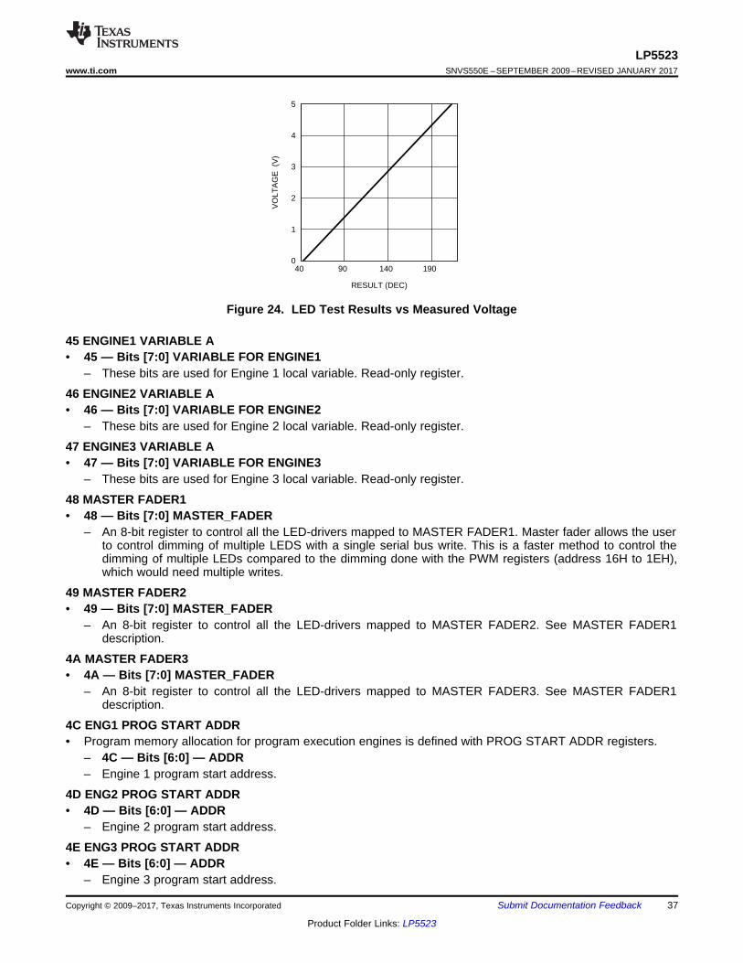
– This is used to store the LED test result. Read-only register. LED test ADC's least significant bitcorresponds to 30 mV. The measured voltage V (typical) is calculated as follows: V = (RESULT(DEC) ×0.03 – 1.478 V. For example, if the result is 10100110 = 166(DEC), the measured voltage is 3.5 V(typical). See Figure 24.
– These bits are used for Engine 3 local variable. Read-only register.
48 MASTER FADER1• 48 — Bits [7:0] MASTER_FADER
– An 8-bit register to control all the LED-drivers mapped to MASTER FADER1. Master fader allows the userto control dimming of multiple LEDS with a single serial bus write. This is a faster method to control thedimming of multiple LEDs compared to the dimming done with the PWM registers (address 16H to 1EH),which would need multiple writes.
49 MASTER FADER2• 49 — Bits [7:0] MASTER_FADER
– An 8-bit register to control all the LED-drivers mapped to MASTER FADER2. See MASTER FADER1description.
4A MASTER FADER3• 4A — Bits [7:0] MASTER_FADER
– An 8-bit register to control all the LED-drivers mapped to MASTER FADER3. See MASTER FADER1description.
4C ENG1 PROG START ADDR• Program memory allocation for program execution engines is defined with PROG START ADDR registers.
– These bits select the program memory page. The program memory is divided into six pages of 16instructions; thus, the total amount of the program memory is 96 instructions.
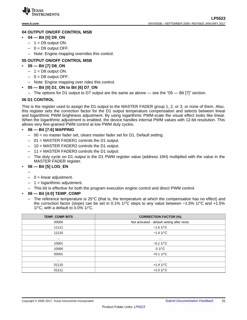
70H ENG1 MAPPING MSB• Valid engine 1-to-LED -mapping information can be read from ENG1 MAPPING register.• 70H — Bit [7] GPO
– 1 = GPO pin is mapped to the program execution engine 1.– 0 = GPO pin non-mapped to the program execution engine 1.
• 70H — Bit [0] D9– 1 = D9 pin is mapped to the program execution engine 1.– 0 = D9 pin non-mapped to the program execution engine 1.
71H ENG1 MAPPING LSB• 71H — Bit [7] D8
– 1 = D8 pin is mapped to the program execution engine 1.– 0 = D8 pin non-mapped to the program execution engine 1.
• 71H — Bit [6] D7– 1 = D7 pin is mapped to the program execution engine 1.– 0 = D7 pin non-mapped to the program execution engine 1.
• 71H — Bit [5] D6– 1 = D6 pin is mapped to the program execution engine 1.– 0 = D6 pin non-mapped to the program execution engine 1.
• 71H — Bit [4] D5– 1 = D5 pin is mapped to the program execution engine 1.– 0 = D5 pin non-mapped to the program execution engine 1.
• 71H — Bit [3] D4– 1 = D4 pin is mapped to the program execution engine 1.– 0 = D4 pin non-mapped to the program execution engine 1.
• 71H — Bit [2] D3– 1 = D3 pin is mapped to the program execution engine 1.– 0 = D3 pin non-mapped to the program execution engine 1.
• 71H — Bit [1] D2– 1 = D2 pin is mapped to the program execution engine 1.– 0 = D2 pin non-mapped to the program execution engine 1.
• 71H — Bit [0] D1– 1 = D1 pin is mapped to the program execution engine 1.– 0 = D1 pin non-mapped to the program execution engine 1.
72H ENG2 MAPPING MSB• Valid engine 2-to-LED-mapping information can be read from ENG2 MAPPING register.• 72H — Bit [7] GPO
– See description above for ENG1 MAPPING register.• 72H — Bit [0] D9
– See previous description for ENG1 MAPPING register.
73H ENG2 MAPPING LSB• 73H — Bit [7] D8 to Bit [0] D1• See previous description for ENG1 MAPPING register.
74H ENG3 MAPPING MSB• Valid engine 3-to-LED -mapping information can be read from ENG3 MAPPING register.
• 74H — Bit [7] GPO– See description above for ENG1 MAPPING register.
• 74H — Bit [0] D9– See description above for ENG1 MAPPING register.
75H ENG3 MAPPING LSB• 75H — Bit [7] D8 to Bit [0] D1
– See previous description for ENG1 MAPPING register.
76H GAIN_CHANGE_CTRL• With hysteresis and timer bits the user can optimize the charge pump performance to better meet the
requirements of the application at hand. Some applications need to be optimized for efficiency and othersneed to be optimized for minimum EMI, for example.
• 76H - Bits[7:6] THRESHOLD– Threshold voltage (typical) pre-setting. Bits set the threshold voltage at which the charge-pump gain
changes from 1.5× to 1×. The threshold voltage is defined as the voltage difference between highestvoltage output (D1 to D6) and input voltage VDD: VTHRESHOLD = VDD – MAX(voltage on D1 to D6).
– If VTHRESHOLD is larger than the set value (100 mV to 400 mV), the charge pump is in 1× mode.– 00 = 400 mV– 01 = 300 mV– 10 = 200 mV– 11 = 100 mV–
NOTEValues above are typical and should not be used as product-specification.
NOTEWriting to threshold [7:6] bits by the user overrides factory settings. Factory settings aren'tuser-accessible.
Gain-change hysteresis prevents the mode from toggling back and forth (1× -> 1.5× -> 1x...) , which wouldcause ripple on VIN and LED flicker. When the adaptive threshold is enabled, the width of the hysteresisregion depends on the choice of threshold bits (see above), saturation of the current sources, chargepump load current, PWM overlap and temperature.
• 76H - Bits [4:3] TIMER• A forced mode change from 1.5× to 1× is attempted at the interval specified with these bits. Mode change is
allowed if there is enough voltage over the LED drivers to ensure proper operation. Set FORCE_1x to 1 (seefollowing 76H - Bit [2] FORCE_1x) to activate this feature.– 00 = 5 ms– 01 = 10 ms– 10 = 50 ms– 11 = infinite. The charge pump switches gain from 1× mode to 1.5× mode only. The gain reset back to 1×
is enabled under certain conditions, for example in the powersave mode.•• Activates forced mode change. In forced mode, charge pump mode change from 1.5× to 1× is attempted at
the constant interval specified with the TIMER bits.– 1 = forced-mode changes enabled– 0 = forced-mode changes disabled
(1) This opcode is used with numerical operands.(2) This opcode is used with variables.
7.6.3 Instruction SetThe LP5523 has three independent programmable execution engines. All the program execution engines havetheir own program memory block allocated by the user. Note that in order to access program memory theoperation mode needs to be load program, at least for one of the three program execution engines. Programexecution is clocked with a 32.7-kHz clock. This clock can be generated internally or external 32-kHz clock canbe connected to CLK pin. Using external clock enables synchronization of LED timing to the external clocksignal.
Supported instruction set is listed in the following tables:
Table 4. LP5523 LED Driver Instructions
Inst. Bit[15]
Bit[14]
Bit[13]
Bit[12]
Bit[11]
Bit[10] Bit [9] Bit [8] Bit
[7] Bit [6] Bit [5] Bit [4] Bit [3] Bit [2] Bit [1] Bit [0]
ramp (1) 0 pre-scale step time sign number of increments
ramp (2) 1 0 0 0 0 1 0 0 0 0 pre-scale sign step time no. of
7.6.4.1 RampThis is the instruction useful for smoothly changing from one PWM value into another PWM value on the D1 toD9 outputs; in other words, generating ramps (with a negative or positive slope). The LP5523 allowsprogramming very fast and very slow ramps.
Ramp instruction generates a PWM ramp, using the effective PWM value as a starting value. At each ramp stepthe output is incremented/decremented by one unit, unless the number of increments is 0. Time span for oneramp step is defined with prescale bit [14] and step time bits [13:9]. Prescale = 0 sets 0.49 ms cycle time andprescale = 1 sets 15.6 ms cycle time; so the minimum time span for one step is 0.49 ms (prescale × step timespan = 0.49 ms × 1) and the maximum time span is 15.6 ms × 31 = 484 ms/step.
Number of increments value defines how many steps are taken during one ramp instruction; increment maximumvalue is 255d, which corresponds increment from zero value to the maximum value. If PWM reachesminimum/maximum value (0/255) during the ramp instruction, ramp instruction is executed to the end regardlessof saturation. This enables ramp instruction to be used as a combined ramp and wait instruction. Note: Rampinstruction is wait instruction when the increment bits [7:0] are set to zero.
(1) Valid for numerical operands.(2) Valid for variables.
Programming ramps with variables is very similar to programming ramps with numerical operands. The onlydifference is that step time and number of increments are captured from variable registers, when the instructionexecution is started. If the variables are updated after starting the instruction execution, it has no effect oninstruction execution. Again, at each ramp step the output is incremented/decremented by one unless incrementis 0. Time span for one step is defined with prescale and step time bits. Step time is defined with variable A, B, Cor D. Variables A, B and C are set with ld-instruction. Variable D is a global variable and can be set by writing theVARIABLE register (address 3C). LED TEST ADC register (address 42) can be used as a source for the variableD, as well. Note: Variable A is the only local variable that can be read throughout the serial bus. Of course, thevariable stored in 3CH can be read (and written) as well.
Setting register 06H, 07H, or 08H bit LOG_EN high/low sets logarithmic (1) or linear ramp (0). By using thelogarithmic ramp setting the visual effect appears like a linear ramp, because the human eye behaves in alogarithmic way.
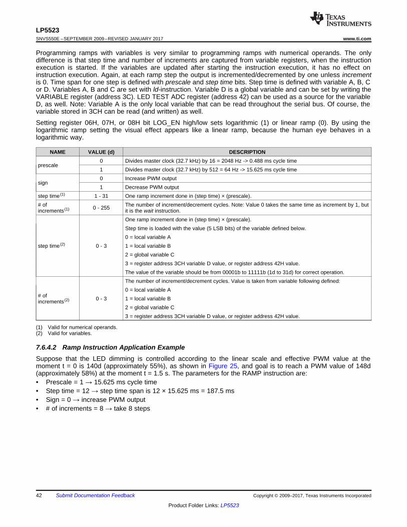
NAME VALUE (d) DESCRIPTION
prescale0 Divides master clock (32.7 kHz) by 16 = 2048 Hz -> 0.488 ms cycle time1 Divides master clock (32.7 kHz) by 512 = 64 Hz -> 15.625 ms cycle time
sign0 Increase PWM output1 Decrease PWM output
step time (1) 1 - 31 One ramp increment done in (step time) × (prescale).# ofincrements (1) 0 - 255 The number of increment/decrement cycles. Note: Value 0 takes the same time as increment by 1, but
it is the wait instruction.
step time (2) 0 - 3
One ramp increment done in (step time) × (prescale).Step time is loaded with the value (5 LSB bits) of the variable defined below.0 = local variable A1 = local variable B2 = global variable C3 = register address 3CH variable D value, or register address 42H value.The value of the variable should be from 00001b to 11111b (1d to 31d) for correct operation.
# ofincrements (2) 0 - 3
The number of increment/decrement cycles. Value is taken from variable following defined:0 = local variable A1 = local variable B2 = global variable C3 = register address 3CH variable D value, or register address 42H value.
7.6.4.2 Ramp Instruction Application ExampleSuppose that the LED dimming is controlled according to the linear scale and effective PWM value at themoment t = 0 is 140d (approximately 55%), as shown in Figure 25, and goal is to reach a PWM value of 148d(approximately 58%) at the moment t = 1.5 s. The parameters for the RAMP instruction are:• Prescale = 1 → 15.625 ms cycle time• Step time = 12 → step time span is 12 × 15.625 ms = 187.5 ms• Sign = 0 → increase PWM output• # of increments = 8 → take 8 steps
(1) Valid for numerical operands.(2) Valid for variables.
Figure 25. Example of Ramp Instruction
7.6.4.3 Set_PWMThis instruction is used for setting the PWM value on the outputs D1 to D9 without any ramps. Set PWM outputvalue from 0 to 255 with PWM value bits [7:0]. Instruction execution takes sixteen 32 kHz clock cycles (=488 µs).
NAME VALUE (d) DESCRIPTIONPWM value (i) (1) 0 - 255 PWM output duty cycle 0 - 100%
variable (ii) (2) 0 - 3
0 = local variable A1 = local variable B2 = global variable C3 = register address 3CH variable D value, or register address 42H value.
7.6.4.4 WaitWhen a wait instruction is executed, the engine is set in wait status, and the PWM values on the outputs arefrozen.
NAME VALUE (d) DESCRIPTION
prescale0 Divide master clock (32.7 kHz) by 16 which means 0.488-ms cycle time.1 Divide master clock (32 768 Hz) by 512 which means 15.625-ms cycle time.
time 1 - 31 Total wait time is = (time) × (prescale). Maximum 484 ms, minimum 0.488 ms.
7.6.5 LED Mapping InstructionsThese instructions define the engine-to-LED mapping. The mapping information is stored in a table, which isstored in the SRAM (program memory of the LP5523). LP5523 has three program execution engines which canbe mapped to 9 LED drivers or to one GPO pin. One engine can control one or multiple LED drivers. There aretotally eleven instructions for the engine-to-LED-driver control: mux_ld_start, mux_map_start, mux_ld_end,mux_sel, mux_clr, mux_map_next, mux_map_prev, mux_ld_next, mux_ld_prev, mux_ld_addr andmux_map_addr.
MUX_LD_START; MUX_LD_ENDMux_ld_start and mux_ld_end define the mapping table location in the memory.
NAME VALUE (d) DESCRIPTIONSRAM address 0-95 Mapping table start/end address
MUX_MAP_STARTMux_map_start defines the mapping table start address in the memory, and the first row of the table is activated(mapped) at the same time.
NAME VALUE (d) DESCRIPTIONSRAM address 0-95 Mapping table start address
MUX_SELWith mux_sel instruction one, and only one, LED driver (or the GPO-pin) can be connected to a programexecution engine. Connecting multiple LEDs to one engine is done with the mapping table. After the mappinghas been released from an LED, PWM register value still controls the LED brightness. If the mapping is releasedfrom the GPO pin, serial bus control takes over the GPO state.
MUX_CLRMux_clr clears engine-to-driver mapping. After the mapping has been released from an LED, the PWM registervalue still controls the LED brightness. If the mapping is released from the GPO pin, serial bus control takes overthe GPO state.
MUX_MAP_NEXTThis instruction sets the next row active in the mapping table each time it is called. For example, if the 2nd row isactive at this moment, after mux_map_next instruction call the 3rd row is active. If the mapping table endaddress is reached, activation rolls to the mapping table start address next time when the mux_map_nextinstruction is called. Engine does not push a new PWM value to the LED driver output before set_pwm or rampinstruction is executed. If the mapping has been released from an LED, the value in the PWM register stillcontrols the LED brightness. If the mapping is released from the GPO pin, serial bus control takes over the GPOstate.
MUX_LD_NEXTSimilar than the mux_map_next instruction, but only the index pointer is set to point to the next row; that is, nomapping is set, and the engine-to-LED-driver connection is not updated.
This instruction sets the previous row active in the mapping table each time it is called. For example, if the 3rdrow is active at this moment, after mux_map_prev instruction call the 2nd row is active. If the mapping table startaddress is reached, activation rolls to the mapping table end address next time the mux_map_prev instruction iscalled. Engine does not push a new PWM value to the LED driver output before set_pwm or ramp instruction isexecuted. If the mapping has been released from an LED, the value in the PWM register still controls the LEDbrightness. If the mapping is released from the GPO pin, serial bus control takes over the GPO state.
MUX_LD_PREVSimilar than the mux_map_prev instruction, but only the index pointer is set to point to the previous row; that is,no mapping is set, and the engine-to-LED-driver connection is not updated.
MUX_MAP_ADDRMux_map_addr sets the index pointer to point the mapping table row defined by bits [6:0] and sets the rowactive. Engine does not push a new PWM value to the LED driver output before set_pwm or ramp instruction isexecuted. If the mapping has been released from an LED, the value in the PWM register still controls the LEDbrightness. If the mapping is released from the GPO pin, serial bus control takes over the GPO state.
NAME VALUE (d) DESCRIPTIONSRAM address 0-95 Any SRAM address containing mapping data.
MUX_LD_ADDRMux_ld_addr sets the index pointer to point the mapping table row defined by bits [6:0], but the row is not setactive.
NAME VALUE (d) DESCRIPTIONSRAM address 0-95 Any SRAM address containing mapping data.
(1) Valid for numerical operands.(2) Valid for variables.
7.6.6 Branch InstructionsBRANCHBranch instruction is mainly indented for repeating a portion of the program code several times. Branchinstruction loads step number value to program counter. Loop count parameter defines how many times theinstructions inside the loop are repeated. The LP5523 supports nested looping; that is, loop inside loop. Thenumber of nested loops is not limited. Instruction takes sixteen 32 kHz clock cycles.
NAME ACCEPTED VALUE (d) DESCRIPTIONloop count (1) 0-63 The number of loops to be done. 0 means an infinite loop.step number 0-95 The step number to be loaded to program counter.
loop count (2) 0-3
Selects the variable for loop count value. Loop count is loaded with the value of thevariable defined below.0 = local variable A1 = local variable B2 = global variable C3 = register address 3CH variable D value, or register address 42H value
INTSend interrupt to processor by pulling the INT pin down and setting corresponding status bit high. Interrupt canbe cleared by reading interrupt bits in STATUS/INTERRUPT register at address 3A.
0 No interrupt is sent. PWM register values remain intact.
1
Reset program counter value to 0 and send interrupt to processor by pulling the INT pin downand setting corresponding status bit high to notify that program has ended. PWM registervalues remains intact. Interrupt can be cleared by reading interrupt bits inSTATUS/INTERRUPT register at address 3A.
reset
0 Reset program counter value to 0 and hold. PWM register values remains intact.
1
Reset program counter value to 0 and hold. PWM register values of the non-mapped driversremains. PWM register values of the mapped drivers is set to 0000 0000.On completion of int instruction with this bit set to 1 the master fader registers are set to zeroas follows: Program execution engine 1 sets MASTER FADER 1 (48H) to zero, engine 2 setsMASTER FADER 2 (49H) to zero and engine 3 sets MASTER FADER 3 (4AH) to zero.
RSTRst instruction resets Program Counter register (address 37H, 38H, or 39H) and continues executing theprogram from the program start address defined in 4C-4E. Instruction takes sixteen 32 kHz clock cycles. Notethat default value for all program memory registers is 0000H, which is the rst instruction.
ENDEnd program execution. Instruction takes sixteen 32-kHz clock cycles.
TRIGGERWait or send triggers can be used to, for example, synchronize operation between the program executionengines. Send trigger instruction takes sixteen 32 kHz clock cycles and wait for trigger takes at least sixteen 32kHz clock cycles. The receiving engine stores the triggers which have been sent. Received triggers are clearedby wait for trigger instruction. Wait for trigger instruction is executed until all the defined triggers have beenreceived. (Note: several triggers can be defined in the same instruction.)
External trigger input signal must stay low for at least two 32 kHz clock cycles to be executed. Trigger outputsignal is three 32 kHz clock cycles long. External trigger signal is active low; that is, when trigger is sent/receivedthe pin is pulled to GND. Send external trigger is masked; that is, the device that has sent the trigger does notrecognize it. If send and wait external trigger are used on the same instruction, the send external trigger isexecuted first, then the wait external trigger.
NAME VALUE (d) DESCRIPTION
wait for trigger 0 - 31Wait for trigger from the engine(s). Several triggers can be defined in the same instruction. Bit[7] engages engine 1, bit [8] engine 2, bit [9] engine 3 and bit [12] is for external trigger I/O.Bits [10] and [11] are not in use.
send a trigger 0 - 31Send a trigger to the engine(s). Several triggers can be defined in the same instruction. Bit [1]engages engine 1, bit [2] engine 2, bit [3] engine 3 and bit [6] is for external trigger I/O. Bits [4]and [5] are not in use.
The LP5523 instruction set includes the following conditional jump instructions: jne (jump if not equal); jge (jumpif greater or equal); jl (jump if less); je (jump if equal). If the condition is true, a certain number of instructions areskipped (that is, the program jumps forward to a location relative to the present location). If condition is false, thenext instruction is executed.
NAME VALUE (d) DESCRIPTIONnumber of instructions to beskipped if the operation returnstrue.
0 - 31 The number of instructions to be skipped when the statement is true. Note: value 0means redundant code.
variable 1 0 - 3
Defines the variable to be used in the test:0 = local variable A1 = local variable B2 = global variable C3 = register address 3CH variable, or register address 42H value.
Defines the variable to be used in the test:0 = local variable A1 = local variable B2 = global variable C3 = register address 3CH variable, or register address 42H value.
7.6.7 Arithmetic InstructionsLDThis instruction is used to assign a value into a variable; the previous value in that variable is overwritten. Eachof the engines have two local variables, called A and B. The variable C is a global variable.
(1) Valid for numerical operands.(2) Valid for variables.
ADDOperator either adds 8-bit value to the current value of the target variable, or adds the value of the variable 1 (A,B, C or D) to the value of the variable 2 (A, B, C or D) and stores the result in the register of variable A, B or C.Variables overflow from 255 to 0.
NAME VALUE (d) DESCRIPTION8-bit value (1) 0 - 255 The value to be added.
(1) Valid for numerical operands.(2) Valid for variables.
SUBSUB Operator either subtracts 8-bit value from the current value of the target variable, or subtracts the value ofthe variable 2 (A, B, C or D) from the value of the variable 1 (A, B, C or D) and stores the result in the register oftarget variable (A, B or C). Variables overflow from 0 to 255.
NAME VALUE (d) DESCRIPTION8-bit value (1) 0 - 255 The value to be added.
NOTEInformation in the following applications sections is not part of the TI componentspecification, and TI does not warrant its accuracy or completeness. TI’s customers areresponsible for determining suitability of components for their purposes. Customers shouldvalidate and test their design implementation to confirm system functionality.
8.1 Application InformationThe LP5523 enables up to four parallel devices together, which can drive up to 12 RGB LEDs or 36 single LEDs.Figure 26 shows the connections for two LP5523 devices for six RGB LEDs. Note that D7, D8, and D9 outputsare used for the red LEDs. The SCL and SDA lines must each have a pullup resistor placed somewhere on theline (R3 and R4; the pullup resistors are normally located on the bus master.). In typical applications, values of1.8 kΩ to 4.7 kΩ are used, depending on the bus capacitance, I/O voltage, and the desired communicationspeed. INT and TRIG are open-drain pins, which must have pullup resistors. Typical values for R1 and R2 arefrom 120 kΩ to 180 kΩ for two devices.
8.2 Typical Applications
8.2.1 Using Two LP5523 Devices in Same ApplicationThe LP5523 enables up to four parallel devices together, which can drive up to 12 RGB LEDs or 36 single LEDs.This diagram shows the connections for two LP5523 devices for six RGB LEDs. Note that D7, D8 and D9outputs are used for the red LEDs. The SCL and SDA lines must each have a pullup resistor placed somewhereon the line (R3 and R4; The pullup resistors are normally located on the bus master.). In typical applicationsvalues of 1.8 kΩ to 4.7 kΩ are used, depending on the bus capacitance, I/O voltage, and the desiredcommunication speed. INT and TRIG are open-drain pins, so they must have pullup resistors. Typical values forR1 and R2 are from 120 k to 180 k for two devices.
The LP5523 requires 4 external capacitors for proper operation. Surface-mount multi-layer ceramic capacitorsare recommended. Tantalum and aluminium capacitors are not recommended because of their high ESR. Forthe flying capacitors (C1 and C2) always use multi-layer ceramic capacitors. These capacitors are small,inexpensive, and have very low equivalent series resistance (ESR < 20 mΩ typical). Ceramic capacitors withX7R or X5R temperature characteristic are preferred for use with the LP5523. These capacitors have tightcapacitance tolerance (as good as ±10%) and hold their value over temperature (X7R: ±15% over −55°C to+125°C; X5R: ±15% over −55°C to +85°C). Capacitors with Y5V or Z5U temperature characteristic are generallynot recommended for use with the LP5523. Capacitors with these temperature characteristics typically have widecapacitance tolerance (+80%, −20%) and vary significantly over temperature (Y5V: +22%, −82% over −30°C to+85°C range; Z5U: +22%, −56% over 10°C to 85°C range). Under some conditions, a nominal 1 μF Y5V or Z5Ucapacitor could have a capacitance of only 0.1 μF. Such detrimental deviation is likely to cause Y5V and Z5Ucapacitors to fail to meet the minimum capacitance requirements of the LP5523.
For proper operation it is necessary to have at least 0.24 µF of effective capacitance for each of the flyingcapacitors under all operating conditions. The output capacitor COUT directly affects the magnitude of the outputripple voltage. In general, the higher the value of COUT, the lower the output ripples magnitude. For properoperation TI recommends having at least 0.50 µF of effective capacitance for CIN and COUT under all operatingconditions. The voltage rating of all four capacitors must be 6.3 V; 10 V is recommended.
Table 8 lists recommended external components from some leading ceramic capacitor manufacturers. It isstrongly recommended that the LP5523 circuit be thoroughly evaluated early in the design-in process with themass-production capacitors of choice. This helps ensure that any variability in capacitance does not negativelyimpact circuit performance.
Table 8. Recommended External ComponentsMODEL TYPE VENDOR VOLTAGE RATING PACKAGE SIZE
Figure 27. Line Transient and Charge-Pump AutomaticGain Change (1.5× To 1×)
6 LEDs at 1 mA ,100% PWM
Figure 28. Line Transient and Charge-Pump AutomaticGain Change (1× To 1.5×)
8.2.2 Driving Haptic Feedback with LP5523
Figure 29. Example Schematic – Vibra Motor
Figure 29 depicts an example schematic for LP5523 driving a vibra motor. A vibra motor can be used for hapticfeedback with touch screens and also for normal vibra operation (call indication, etc.). Battery-powered D8 andD9 outputs are used for controlling the H-driver (Microchip TC442x-series or equivalent), which drives the vibramotor. (The remaining outputs D1 to D7 can be used for LED driving, of course.) With H-driver the rotationdirection of the vibra motor can be changed. For vibra operation user can load several programs to the LP5523program memory in order to get interesting vibration effects, with changing frequency, ramps, etc.
If the application processor has controls for a vibra motor they can be connected to H-Driver INA and INB asshown in Figure 29. In this case the vibra can be controlled directly with application processor and also withLP5523. If application processor control is not needed, then the 100-kΩ resistors should be connected to GND.
A simple waveform for H-driver control is shown in Figure 30. At first the motor rotates in CW direction for 30 ms,following a rotation of 30 ms in CCW direction. The sequence is started when the TRIG signal is pulled down(active low signal). the TRIG signal is received from the touch screen controller. After the sequence is executed,the LP5523 waits for another TRIG signal to start the sequence again. TRIG signal timing is not critical; it doesnot have to be pulled down for the whole sequence duration like in the example. For call indication, etc. purposesthe program can be changed; for example, rotation times can be adjusted to get desired haptic reaction. Directcontrol of D8 and D9 output is also possible through the control registers, if programming is not desired.
Figure 30. H-Driver Control Waveform
9 Power Supply RecommendationsThe device is designed to operate from an input voltage supply range between 2.7 V and 5.5 V. In a typicalapplication this is from single Li-ion battery cell. This input supply must be well regulated and able to withstandmaximum input current and maintain stable voltage without voltage drop even at load transition condition (start-up or rapid brightness change). The resistance of the input supply rail must be low enough that the input currenttransient does not cause drop below a 2.7-V level in the LP5523 supply voltage.
10.1 Layout GuidelinesPlace capacitors as close as possible to the LP5523 device to minimize the current loops. Example of LP5523PCB layout and component placement is seen in Figure 31.
11.1.1 Third-Party Products DisclaimerTI'S PUBLICATION OF INFORMATION REGARDING THIRD-PARTY PRODUCTS OR SERVICES DOES NOTCONSTITUTE AN ENDORSEMENT REGARDING THE SUITABILITY OF SUCH PRODUCTS OR SERVICESOR A WARRANTY, REPRESENTATION OR ENDORSEMENT OF SUCH PRODUCTS OR SERVICES, EITHERALONE OR IN COMBINATION WITH ANY TI PRODUCT OR SERVICE.
11.2 Receiving Notification of Documentation UpdatesTo receive notification of documentation updates, navigate to the device product folder on ti.com. In the upperright corner, click on Alert me to register and receive a weekly digest of any product information that haschanged. For change details, review the revision history included in any revised document.
11.3 Community ResourcesThe following links connect to TI community resources. Linked contents are provided "AS IS" by the respectivecontributors. They do not constitute TI specifications and do not necessarily reflect TI's views; see TI's Terms ofUse.
TI E2E™ Online Community TI's Engineer-to-Engineer (E2E) Community. Created to foster collaborationamong engineers. At e2e.ti.com, you can ask questions, share knowledge, explore ideas and helpsolve problems with fellow engineers.
Design Support TI's Design Support Quickly find helpful E2E forums along with design support tools andcontact information for technical support.
11.4 TrademarksE2E is a trademark of Texas Instruments.All other trademarks are the property of their respective owners.
11.5 Electrostatic Discharge CautionThis integrated circuit can be damaged by ESD. Texas Instruments recommends that all integrated circuits be handled withappropriate precautions. Failure to observe proper handling and installation procedures can cause damage.
ESD damage can range from subtle performance degradation to complete device failure. Precision integrated circuits may be moresusceptible to damage because very small parametric changes could cause the device not to meet its published specifications.
11.6 GlossarySLYZ022 — TI Glossary.
This glossary lists and explains terms, acronyms, and definitions.
12 Mechanical, Packaging, and Orderable InformationThe following pages include mechanical, packaging, and orderable information. This information is the mostcurrent data available for the designated devices. This data is subject to change without notice and revision ofthis document. For browser-based versions of this data sheet, refer to the left-hand navigation.
LP5523TM/NOPB ACTIVE DSBGA YFQ 25 250 Green (RoHS& no Sb/Br)
SNAGCU Level-1-260C-UNLIM -30 to 85 5523
LP5523TMX/NOPB ACTIVE DSBGA YFQ 25 3000 Green (RoHS& no Sb/Br)
SNAGCU Level-1-260C-UNLIM -30 to 85 5523
(1) The marketing status values are defined as follows:ACTIVE: Product device recommended for new designs.LIFEBUY: TI has announced that the device will be discontinued, and a lifetime-buy period is in effect.NRND: Not recommended for new designs. Device is in production to support existing customers, but TI does not recommend using this part in a new design.PREVIEW: Device has been announced but is not in production. Samples may or may not be available.OBSOLETE: TI has discontinued the production of the device.
(2) Eco Plan - The planned eco-friendly classification: Pb-Free (RoHS), Pb-Free (RoHS Exempt), or Green (RoHS & no Sb/Br) - please check http://www.ti.com/productcontent for the latest availabilityinformation and additional product content details.TBD: The Pb-Free/Green conversion plan has not been defined.Pb-Free (RoHS): TI's terms "Lead-Free" or "Pb-Free" mean semiconductor products that are compatible with the current RoHS requirements for all 6 substances, including the requirement thatlead not exceed 0.1% by weight in homogeneous materials. Where designed to be soldered at high temperatures, TI Pb-Free products are suitable for use in specified lead-free processes.Pb-Free (RoHS Exempt): This component has a RoHS exemption for either 1) lead-based flip-chip solder bumps used between the die and package, or 2) lead-based die adhesive used betweenthe die and leadframe. The component is otherwise considered Pb-Free (RoHS compatible) as defined above.Green (RoHS & no Sb/Br): TI defines "Green" to mean Pb-Free (RoHS compatible), and free of Bromine (Br) and Antimony (Sb) based flame retardants (Br or Sb do not exceed 0.1% by weightin homogeneous material)
(3) MSL, Peak Temp. - The Moisture Sensitivity Level rating according to the JEDEC industry standard classifications, and peak solder temperature.
(4) There may be additional marking, which relates to the logo, the lot trace code information, or the environmental category on the device.
(5) Multiple Device Markings will be inside parentheses. Only one Device Marking contained in parentheses and separated by a "~" will appear on a device. If a line is indented then it is a continuationof the previous line and the two combined represent the entire Device Marking for that device.
(6) Lead/Ball Finish - Orderable Devices may have multiple material finish options. Finish options are separated by a vertical ruled line. Lead/Ball Finish values may wrap to two lines if the finishvalue exceeds the maximum column width.
Important Information and Disclaimer:The information provided on this page represents TI's knowledge and belief as of the date that it is provided. TI bases its knowledge and belief on informationprovided by third parties, and makes no representation or warranty as to the accuracy of such information. Efforts are underway to better integrate information from third parties. TI has taken andcontinues to take reasonable steps to provide representative and accurate information but may not have conducted destructive testing or chemical analysis on incoming materials and chemicals.TI and TI suppliers consider certain information to be proprietary, and thus CAS numbers and other limited information may not be available for release.
In no event shall TI's liability arising out of such information exceed the total purchase price of the TI part(s) at issue in this document sold by TI to Customer on an annual basis.
A. All linear dimensions are in millimeters. Dimensioning and tolerancing per ASME Y14.5M-1994.B. This drawing is subject to change without notice.
NOTES:
4215084/A 12/12
D0.600±0.075
E
D: Max =
E: Max =
2.29 mm, Min =
2.29 mm, Min =
2.23 mm
2.23 mm
IMPORTANT NOTICE
Texas Instruments Incorporated (TI) reserves the right to make corrections, enhancements, improvements and other changes to itssemiconductor products and services per JESD46, latest issue, and to discontinue any product or service per JESD48, latest issue. Buyersshould obtain the latest relevant information before placing orders and should verify that such information is current and complete.TI’s published terms of sale for semiconductor products (http://www.ti.com/sc/docs/stdterms.htm) apply to the sale of packaged integratedcircuit products that TI has qualified and released to market. Additional terms may apply to the use or sale of other types of TI products andservices.Reproduction of significant portions of TI information in TI data sheets is permissible only if reproduction is without alteration and isaccompanied by all associated warranties, conditions, limitations, and notices. TI is not responsible or liable for such reproduceddocumentation. Information of third parties may be subject to additional restrictions. Resale of TI products or services with statementsdifferent from or beyond the parameters stated by TI for that product or service voids all express and any implied warranties for theassociated TI product or service and is an unfair and deceptive business practice. TI is not responsible or liable for any such statements.Buyers and others who are developing systems that incorporate TI products (collectively, “Designers”) understand and agree that Designersremain responsible for using their independent analysis, evaluation and judgment in designing their applications and that Designers havefull and exclusive responsibility to assure the safety of Designers' applications and compliance of their applications (and of all TI productsused in or for Designers’ applications) with all applicable regulations, laws and other applicable requirements. Designer represents that, withrespect to their applications, Designer has all the necessary expertise to create and implement safeguards that (1) anticipate dangerousconsequences of failures, (2) monitor failures and their consequences, and (3) lessen the likelihood of failures that might cause harm andtake appropriate actions. Designer agrees that prior to using or distributing any applications that include TI products, Designer willthoroughly test such applications and the functionality of such TI products as used in such applications.TI’s provision of technical, application or other design advice, quality characterization, reliability data or other services or information,including, but not limited to, reference designs and materials relating to evaluation modules, (collectively, “TI Resources”) are intended toassist designers who are developing applications that incorporate TI products; by downloading, accessing or using TI Resources in anyway, Designer (individually or, if Designer is acting on behalf of a company, Designer’s company) agrees to use any particular TI Resourcesolely for this purpose and subject to the terms of this Notice.TI’s provision of TI Resources does not expand or otherwise alter TI’s applicable published warranties or warranty disclaimers for TIproducts, and no additional obligations or liabilities arise from TI providing such TI Resources. TI reserves the right to make corrections,enhancements, improvements and other changes to its TI Resources. TI has not conducted any testing other than that specificallydescribed in the published documentation for a particular TI Resource.Designer is authorized to use, copy and modify any individual TI Resource only in connection with the development of applications thatinclude the TI product(s) identified in such TI Resource. NO OTHER LICENSE, EXPRESS OR IMPLIED, BY ESTOPPEL OR OTHERWISETO ANY OTHER TI INTELLECTUAL PROPERTY RIGHT, AND NO LICENSE TO ANY TECHNOLOGY OR INTELLECTUAL PROPERTYRIGHT OF TI OR ANY THIRD PARTY IS GRANTED HEREIN, including but not limited to any patent right, copyright, mask work right, orother intellectual property right relating to any combination, machine, or process in which TI products or services are used. Informationregarding or referencing third-party products or services does not constitute a license to use such products or services, or a warranty orendorsement thereof. Use of TI Resources may require a license from a third party under the patents or other intellectual property of thethird party, or a license from TI under the patents or other intellectual property of TI.TI RESOURCES ARE PROVIDED “AS IS” AND WITH ALL FAULTS. TI DISCLAIMS ALL OTHER WARRANTIES ORREPRESENTATIONS, EXPRESS OR IMPLIED, REGARDING RESOURCES OR USE THEREOF, INCLUDING BUT NOT LIMITED TOACCURACY OR COMPLETENESS, TITLE, ANY EPIDEMIC FAILURE WARRANTY AND ANY IMPLIED WARRANTIES OFMERCHANTABILITY, FITNESS FOR A PARTICULAR PURPOSE, AND NON-INFRINGEMENT OF ANY THIRD PARTY INTELLECTUALPROPERTY RIGHTS. TI SHALL NOT BE LIABLE FOR AND SHALL NOT DEFEND OR INDEMNIFY DESIGNER AGAINST ANY CLAIM,INCLUDING BUT NOT LIMITED TO ANY INFRINGEMENT CLAIM THAT RELATES TO OR IS BASED ON ANY COMBINATION OFPRODUCTS EVEN IF DESCRIBED IN TI RESOURCES OR OTHERWISE. IN NO EVENT SHALL TI BE LIABLE FOR ANY ACTUAL,DIRECT, SPECIAL, COLLATERAL, INDIRECT, PUNITIVE, INCIDENTAL, CONSEQUENTIAL OR EXEMPLARY DAMAGES INCONNECTION WITH OR ARISING OUT OF TI RESOURCES OR USE THEREOF, AND REGARDLESS OF WHETHER TI HAS BEENADVISED OF THE POSSIBILITY OF SUCH DAMAGES.Unless TI has explicitly designated an individual product as meeting the requirements of a particular industry standard (e.g., ISO/TS 16949and ISO 26262), TI is not responsible for any failure to meet such industry standard requirements.Where TI specifically promotes products as facilitating functional safety or as compliant with industry functional safety standards, suchproducts are intended to help enable customers to design and create their own applications that meet applicable functional safety standardsand requirements. Using products in an application does not by itself establish any safety features in the application. Designers mustensure compliance with safety-related requirements and standards applicable to their applications. Designer may not use any TI products inlife-critical medical equipment unless authorized officers of the parties have executed a special contract specifically governing such use.Life-critical medical equipment is medical equipment where failure of such equipment would cause serious bodily injury or death (e.g., lifesupport, pacemakers, defibrillators, heart pumps, neurostimulators, and implantables). Such equipment includes, without limitation, allmedical devices identified by the U.S. Food and Drug Administration as Class III devices and equivalent classifications outside the U.S.TI may expressly designate certain products as completing a particular qualification (e.g., Q100, Military Grade, or Enhanced Product).Designers agree that it has the necessary expertise to select the product with the appropriate qualification designation for their applicationsand that proper product selection is at Designers’ own risk. Designers are solely responsible for compliance with all legal and regulatoryrequirements in connection with such selection.Designer will fully indemnify TI and its representatives against any damages, costs, losses, and/or liabilities arising out of Designer’s non-compliance with the terms and provisions of this Notice.