IEEE TRANSACTIONSONELECTRON DEVICES, VOL. ED-18, NO. 7, JULY 1971 [lo] H. W. Thim,[‘Computerstudy of bulk G;As devices with ran-Gunneffect,” Electron. Lett., vo!. 2, June 1966, pp. 194-195. [ll] H. W. Thim and K. Kuykawa, “Quenched bulk GaAs oscillators [12] J. E. Caroll, “Nonuniform motion of high-field domains in the 1969, pp. 537-542. 439 dom one-dimensional doping fluctuations, J. Appl. Phys., vol. [13] K. Kurokawa, “Transient behavlor of high-field domains in bulk 39, July 1968, pp. 3897-3904. semiconductors,” Proc. IEEE (Lett.), vol. 55, Sept. 1967, with doping gradients, J. AppZ. Phys., vol. 40, Feb. 1969, [14] H. D. Rees, Time response of the high-field electron distribu- pp. 1615-161$. pp. 904-906. tion function in GaAs,” IBX J. Res. Develop., vol. 13, Sept. LSA Relaxation Oscillator Principles Abstract-Oversized n-GaAs diodes operating in the LSA mode with doping-to-frequency ratios inthe 1-5X10⁶ s/cm3 range are investigated in circuits that contain a short-circuited high impedance transmission line foreshortened to resonate the electronic parallel capacitance of the diode. By comparing computer simulations with experiments, such diodes are shown to operate in a nonsinusoidal LSA relaxation mode which offers good efficiency, effective space- charge control, and a fast buildup of the oscillations; details of the computerprogram are alsogiven. A simpleanalysis is developed which defines the inductive and capacitive time constants controlling the voltage waveshape and explains the frequency tuning with bias voltage and the effective space-charge control. The analysis is shown to be suitable for oscillator design purposes. I. INTRODUCTIOX A experimental and theoretical investigation of oversized n-GaAs diodes operating in the LSA mode with doping-to-frequency ratios in the 1-5 x10⁵ s/cm3 range will be discussed in this paper. The LSA mode was first proposed by Copeland [l]. Forasinusoidalvoltagewaveshapeacrossthediode, Copeland [2] later calculated the usable range for the doping-to-frequency ratio to 2 X 10⁴-2 X lo5 s/cm3 and the maximum attainable dc to RF conversion efficiency to 18 percent for a doping-to-frequency ratio of 6 X lo4 s/cm3, As the experimental efficiencies for a long time were considerably lower than the predicted 18 percent, Copeland [3] and Thim and Kurokawa [4], [5] in- vestigated in computer simulations the degradation of the efficiency for the sinusoidal LSA mode caused by spatial variations of the doping density in the LSA diode. Those simulations could account for thelow efficiencies observed, but it remained to be explained that the best experimental efficiencies were normally obtained with doping-to-frequency ratios well above the predicted optimal value [6] and that a strong content of higher harmonics in the device voltage waveshape was ob- conducted while the authors were with Cayuga Associates, Inc., Manuscript received September 14, 1970. Part of this research was Ithaca, N. Y., and Cornel1 University, Ithaca, N. Y. P. Jeppesen is wlth the Laboratory of Electromagnetic Theory, Technical University of Denmark, Lyngby, Denmark. B. I. Jeppsson is with the Microwave Institute, Royal Insti- tute of Technology, Stockholm, Sweden. served [7]. In his LSA oscillator theory, Copeland [Z] hadforeseen that the usable range for the doping-to- frequency ratio as well as the maximum attainable efficiency would depend on the voltage waveshape. Accordingly, it was proposed by the authors [8] that the diodes in the experiments referred to above, oper- ated in an LSA mode, or in a mode with an accumula- tion layer sweeping through most of the active region in a short diode, as computer simulations in a multi- resonant circuit revealed that LSA oscillations could be retained for doping-to-frequency ratios up to about 1 X lo8 s/cm3 with some sacrifice in efficiency. Shortly thereafter, Reynolds et al. [9] reported an experimental efficiency around 30 percent at L-band frequencies using a doping-to-frequency ratio in the 2-5 X lo5 s/cm3 range. Simultaneously, Copeland [lo] performed numerical calculations, where a voltage waveshape was dictated acrossthediode,andhefoundthatwithapeak-to- valley ratio of 2.8, 30 percent efficiency appeared possi- ble by using the proper second harmonic tuning and that doping-to-frequency ratios below 1 X lo5 s/cm3 should beusedinordertoobtainspace-chargecontrol. The predicted efficiency agrees very well with those ob- tained experimentally, but the method of dictating the preferable voltage waveshape across the diode does not solve the problem of synthesizing the corresponding microwave circuit. It is the purpose of this paper to analyze LSA diodes with doping-to-frequency ratios in the 1-5 X lo5 s/cm3 range and which are mounted in circuits that contain a short-circuited high impedance transmission line foreshortened to resonate the electronic parallel capaci- tance of the diode. As pointed out briefly in an earlier letter [ll], such diodes may operate in a nonsinusoidal LSA relaxation mode which offers good efficiency, effec- tive space-charge control, and a fast buildup of the oscillations. The LSA relaxation mode will be investigated by comparing experimental results with results from com- puter simulations and from a simple analytical analysis. In Section I1 of this paper, the first high peak power
Transcript
IEEE TRANSACTIONS ON ELECTRON DEVICES, VOL. ED-18, NO. 7, JULY 1971
[lo] H. W . Thim, [‘Computer study of bulk G;As devices with ran- Gunn effect,” Electron. Lett., vo!. 2 , June 1966, pp. 194-195.
[ll] H. W . Thim and K. Kuykawa, “Quenched bulk GaAs oscillators
[12] J. E. Caroll, “Nonuniform motion of high-field domains in the 1969, pp. 537-542.
439
dom one-dimensional doping fluctuations, J . A p p l . Phys., vol. [13] K. Kurokawa, “Transient behavlor of high-field domains in bulk 39, July 1968, pp. 3897-3904. semiconductors,” Proc. IEEE (Lett.), vol. 55, Sept. 1967,
with doping gradients, J . AppZ. Phys., vol. 40, Feb. 1969, [14] H. D. Rees, Time response of the high-field electron distribu- pp. 1615-161$.
pp. 904-906. tion function in GaAs,” I B X J . Res. Develop., vol. 13, Sept.
LSA Relaxation Oscillator Principles
Abstract-Oversized n-GaAs diodes operating in the LSA mode with doping-to-frequency ratios in the 1-5X10⁶ s/cm3 range are investigated in circuits that contain a short-circuited high impedance transmission line foreshortened to resonate the electronic parallel capacitance of the diode. By comparing computer simulations with experiments, such diodes are shown to operate in a nonsinusoidal LSA relaxation mode which offers good efficiency, effective space- charge control, and a fast buildup of the oscillations; details of the computer program are also given. A simple analysis is developed which defines the inductive and capacitive time constants controlling the voltage waveshape and explains the frequency tuning with bias voltage and the effective space-charge control. The analysis is shown to be suitable for oscillator design purposes.
I. INTRODUCTIOX
A experimental and theoretical investigation of oversized n-GaAs diodes operating in the LSA mode with doping-to-frequency ratios in the
1-5 x10⁵ s/cm3 range will be discussed in this paper. The LSA mode was first proposed by Copeland [l].
For a sinusoidal voltage waveshape across the diode, Copeland [2] later calculated the usable range for the doping-to-frequency ratio to 2 X 10⁴-2 X lo5 s/cm3 and the maximum attainable dc to RF conversion efficiency to 18 percent for a doping-to-frequency ratio of 6 X l o4 s/cm3, As the experimental efficiencies for a long time were considerably lower than the predicted 18 percent, Copeland [ 3 ] and Thim and Kurokawa [4], [5] in- vestigated in computer simulations the degradation of the efficiency for the sinusoidal LSA mode caused by spatial variations of the doping density in the LSA diode. Those simulations could account for the low efficiencies observed, but it remained to be explained that the best experimental efficiencies were normally obtained with doping-to-frequency ratios well above the predicted optimal value [6] and that a strong content of higher harmonics in the device voltage waveshape was ob-
conducted while the authors were with Cayuga Associates, Inc., Manuscript received September 14, 1970. Part of this research was
Ithaca, N. Y., and Cornel1 University, Ithaca, N. Y. P. Jeppesen is wlth the Laboratory of Electromagnetic Theory,
Technical University of Denmark, Lyngby, Denmark. B. I. Jeppsson is with the Microwave Institute, Royal Insti-
tute of Technology, Stockholm, Sweden.
served [7]. In his LSA oscillator theory, Copeland [ Z ] had foreseen that the usable range for the doping-to- frequency ratio as well as the maximum attainable efficiency would depend on the voltage waveshape. Accordingly, it was proposed by the authors [8] that the diodes in the experiments referred to above, oper- ated in an LSA mode, or in a mode with an accumula- tion layer sweeping through most of the active region in a short diode, as computer simulations in a multi- resonant circuit revealed that LSA oscillations could be retained for doping-to-frequency ratios up to about 1 X lo8 s/cm3 with some sacrifice in efficiency. Shortly thereafter, Reynolds et al. [9] reported an experimental efficiency around 30 percent at L-band frequencies using a doping-to-frequency ratio in the 2-5 X lo5 s/cm3 range. Simultaneously, Copeland [lo] performed numerical calculations, where a voltage waveshape was dictated across the diode, and he found that with a peak-to- valley ratio of 2.8, 30 percent efficiency appeared possi- ble by using the proper second harmonic tuning and that doping-to-frequency ratios below 1 X lo5 s/cm3 should be used in order to obtain space-charge control. The predicted efficiency agrees very well with those ob- tained experimentally, but the method of dictating the preferable voltage waveshape across the diode does not solve the problem of synthesizing the corresponding microwave circuit.
I t is the purpose of this paper to analyze LSA diodes with doping-to-frequency ratios in the 1-5 X lo5 s/cm3 range and which are mounted in circuits that contain a short-circuited high impedance transmission line foreshortened to resonate the electronic parallel capaci- tance of the diode. As pointed out briefly in an earlier letter [ll], such diodes may operate in a nonsinusoidal LSA relaxation mode which offers good efficiency, effec- tive space-charge control, and a fast buildup of the oscillations.
T h e LSA relaxation mode will be investigated by comparing experimental results with results from com- puter simulations and from a simple analytical analysis. In Section I1 of this paper, the first high peak power
44.0 IEEE TRANSACTIONS ON ELECTRON DEVICES, JULY 1971
I S A relaxation oscillator is discussed along with some experimental results. Because of the simplicity of this oscillator, it serves well to illustrate the technique of simulating, in a computer, the internal space-charge dynamics within the LSA diode and the diode-circuit interaction. Thus, Section I1 is concluded by a descrip- tion of the computer program, details of which are given in Appendix I. In Section 111, results obtained from the computer simulations are given with emphasis on the mode of operation and selective harmonic load- ing. Section IV is devoted to a simple analysis of the I S A relaxation oscillator and expressions for the voltage waveshape are given; the derivation is outlined in Appendix 11. The simple analysis is shown to explain the basic features of the LSA relaxation mode and to give results in quantitative agreement with experiments and computer simulations. Concluding remarks are contained in Section V.
11. MODEL OF THE FIRST LSA RELAXATION OSCILLATOR
A . The First LSA Relaxation Oscillator Several kilowatts of peak powers have been obtained
from many times oversized LSA diodes with doping- to-frequency ratios in the 1-5 X 10⁶ s/cm3 range [11]- [13]. The diodes were mounted in the X-band wave- guide post structure circuit shown in Fig. l(a) and were oscillating with a fundamental frequency at L band, which could be detected by the magnetic coupling loop inserted through the waveguide wall. Oscillations at the third or fourth harmonic frequency were above the waveguide cutoff frequency and could be tuned with the sliding short behind the diode and the slide screw tuner in front. The best results obtained with three different diodes are summarized in Table I for later use. Here no is the doping density, L, is the length of active region, fl and f4 are the fundamental and fourth harmonic frequencies, PI and Pd are the funda- mental and fourth harmonic output powers, and 71 and 774 are the fundamental and fourth harmonic efficiencies.
B. Model f o r the Oscillator Circuit An equivalent diagram of the waveguide post struc-
ture circuit is shown in Fig. 1 (b). Transmission line 1 represents the slab line formed by the circular post across the waveguide and the side walls. I t has the characteristic impedance Z ~ = 2 0 0 a, the length IL = c / ( 4 f ~ ) where c = 3 X 10'0 cm/s is the velocity of light and f L = 7.5 GHz. At microwave frequencies, i t is al- most short-circuited by Rw = 0.1 a which represents the low impedance wavetrap. The battery voltage VB and transmission line 1 determine primarily the mode of operation and the fundamental frequency. The load- ing of the diode introduced by the coupling loop is represented by RL= 1 ka. Transmission line 2 is of secondary importance for the mode of operation and represents the X-band waveguide. Waveguide disper- sion has been neglected since this phenomenon is not
TABLE I EXPERIXENTAL RESULTS FROM LSA DIODES IK THE
CIRCUIT IX FIG. 1 (a)
no X La (x1013 cm-2) (GHzj .f1 (GHzj s/cmx) (W) (W) (g) (g) f 4 (X106 P I PC
nolf1
3.5 5.3
1.75 7.00 3.6 6000 1.75 7.00 6.0 1450
14.6
4.6 1.75 7.00 4.0 2100 5 . 1 4.0
~
of central importance for the mode of operation. In the experiments, the third or fourth harmonic signals propagating in the waveguide were just above cutoff; hence Z H = 2 ka was chosen for the characteristic im- pedance of transmission line 2. The combined effect of the sliding piston and the slide screw tuner is repre- sented by RT in this model.
I t is convenient to represent the overall load im- pedance presented to the diode by a resistance R ( f ) in parallel with an inductance L ( f ) [Fig. l(c)] both of which depend on the frequency f.
For a small VSWR =RT/ZH, transmission line 2 causes only a negligible perturbation of the overall load impedance. Then equal loading at the fundamental frequency (n = 1) and a t the lowest higher harmonics (n=2,3) results as illustrated in Fig. 2 for the param- eters tabulated in Table 11, line 1. For higher VSWR selective loading, for example at the third harmonic, (n = 3 ) may occur; this is illustrated in Fig. 2 for the parameters in Table 11, line 3.
C. Tvansmiss ion L ine Wave Dynamics In order to perform time domain computer simula-
tions, the circuit must be treated in the time domain and this is done by considering the voltage waves propagat-
JEPPESEN AND JEPPSSON: LSA RELAXATION OSCILLATOR PRINCIPLES 441
(4)
FREQUENCY /fL
Fig. 2. Normalized parallel load resistance versus normalized fre- quency for equivalent diagram in Fig. l(b). Important circuit parameters are given in Table 11, lines 1 and 3.
TABLE I1 CIRCUIT PARAMETERS [FIG. 1 (b)] FOR COMPUTER SIMULATIONS
Fig. 3. Propagating voltage waves alter an arbitrary number of reflections.
ing on the transmission lines as sketched in Fig. 3, where the voltage waves are shown schematically after an arbitrary number of reflections. For the voltage wave propagating on transmission line 1 in the positive direc- tion, Vl,(t) denotes the voltage of this wave at plane A at time t. Since there is no distortion of this wave as i t propagates from plane A to 2 3 , the voltage of this wave a t plane B at time t is Vlpjt- Z L / C ) . By using a similar notation for the other voltage waves Vln(t), Vl,(t-ZL/c), . . , V,,(t -ZR/c), the equations relating those waves t o the diode voltage V(t ) and current I ( t ) become
D. Basic Equations and Assumptions f o r the LSA Diode In order to study the behavior of an LSA diode in the
microwave circuit described above, the basic equations governing the one-dimensional movement of the elec- trons from the cathode to the anode have been used. T h e basic equations are the Poisson equation
and the continuity equation
where - q is the electron charge ( q > O ) ; e is the absolute permittivity of GaAs; D is the diffusion coefficient; x is the position; t is the time; no(%) is the doping density; % ( x , t ) is the electron density; E ( % , t ) is the electric field; and v ( E ) is the electron drift velocity. The x axis is oriented from cathode to anode, v(E) and V( t ) in the same direction, and E and I ( t ) in the opposite one.
As diffusion current densities are normally small com- pared to drift current densities in LSA diodes, the field dependence of the diffusion coefficient has been ne- glected and D = 200 cm2/s has been used.
The electron drift velocity-electric field characteristic has been approximated by [4]
\Eo/ v(E) = -
where pLg=SOOO cm2/Vs, os =0.85 X10⁷ crn/s, and Eo = 4000 V/cm.
The doping density no(%) appearing in (6) and (7) has been prescribed to represent the doping profile. I n the active region, nD(x) may contain a depletion notch, random fluctuations, or a gradient. The contact regions could be modelled by making E D very large in the con- tacts, but in the present investigation the mobility in the contacts was increased instead. This method is more convenient and does not invalidate the simulations
The problem of determining the time space variation of %(x, t ) and E ( x , t ) from ( 6 ) and (7) using the assump- tions above and using suitable initial and boundary conditions was solved numerically by approximating
442
the differential equations with difference equations. The numerical integration, which is outlined in Appendix I , is started when the battery voltage V B is connected to the circuit, and is continued through the first cycles until the starting transients have decayed and the stationary oscillation is reached, in which the diode voltage and current are periodic functions of time. The t ime period i s then determined and the diode voltage and current are Fourier-analyzed in order to determine the dc to R F conversion efficiencies and the electronic admit- tances at the fundamental and at the lowest higher harmonic frequencies.
111. RESULTS FROM COMPUTER SIMULATIONS
A . Equal Loading For the large-signal computer simulations of the first
high peak power LSA relaxation oscillator, diode input da ta were chosen in agreement with the experimental data in Section 11: nOLa =3.O X 1013 cm-2, no/fl = 1.9- 5.0 X lo5 s/cm3, and Ro = 5 a, where Ra is the low field resistance.
The circuit parameters were adjusted to provide equal loading at the fundamental and at the lowest higher harmonic frequencies. The circuit parameters are listed in Table 11, line 1 and R ( f ) versusf is plotted in Fig. 2 as mentioned earlier.
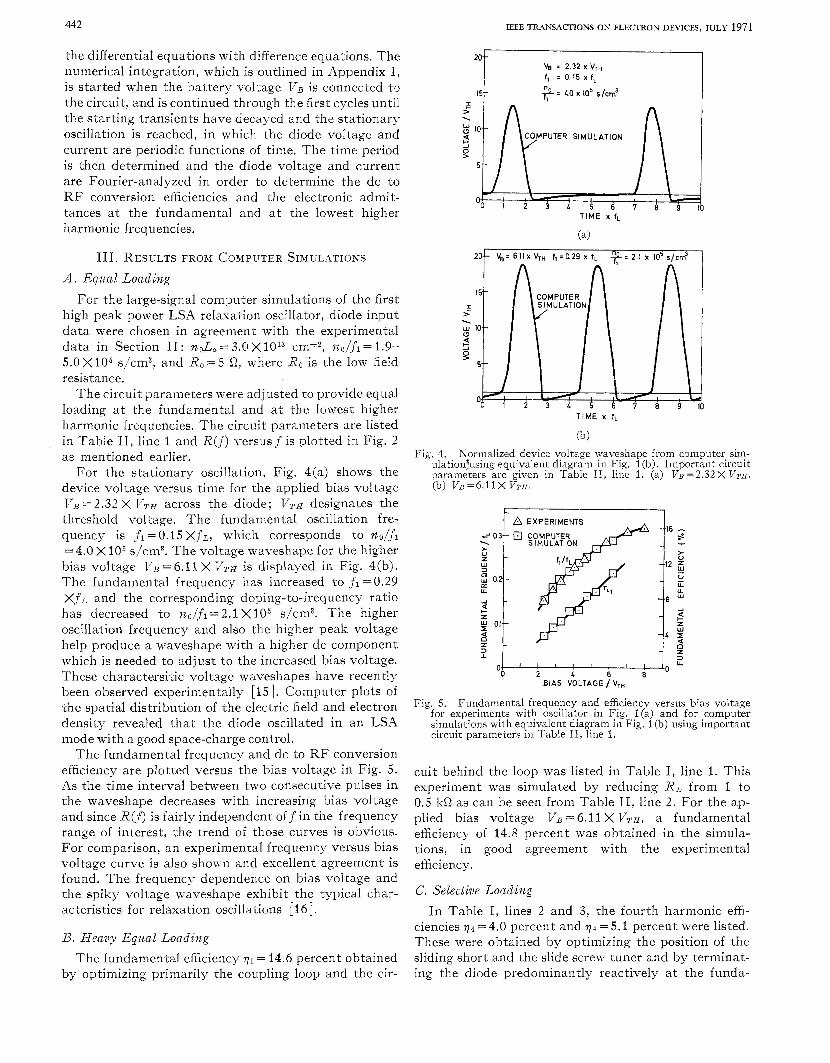
For the stationary oscillation, Fig. 4(a) shows the device voltage versus time for the applied bias voltage VB = 2.32 X VTH across the diode; VTH designates the .threshold voltage. The fundamental oscillation fre- quency is f1= 0.15 X f L , which corresponds to no/fi =4.0 X lo5 s/cm3. The voltage waveshape for the higher bias voltage V B = 6.11 x V T H is displayed in Fig. 4(b). The fundamental frequency has increased to f l=0.29 Xf L and the corresponding doping-to-frequency ratio has decreased, to no/fl= 2.1 XlOj s/cm3. The higher oscillation frequency and also the higher peak voltage help produce a waveshape with a higher dc component which is needed to adjust to the increased bias voltage. These charactersitic voltage waveshapes have recently been observed experimentally [15] . Computer plots of the spatial distribution of the electric field and electron density revealed that the diode oscillated in an LSA mode with a good space-charge control.
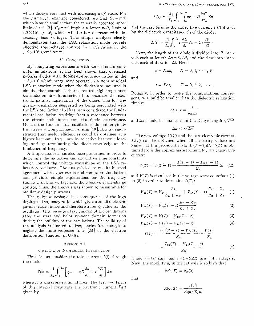
The fundamental frequency and dc to R F conversion efficiency a.re plotted versus the bias voltage in Fig. 5 . As the time interval between two consecutive pulses in the waveshape decreases with increasing bias voltage and since R( f ) is fairly independent off in the frequency range of interest, the trend of those curves is obvious. For comparison, an experimental frequency versus bias voltage curve is also shon-n and excellent agreement is found. The frequency dependence on bias voltage and the spiky voltage waveshape exhibit the typical char- acteristics for relaxation oscillations [16].
B. Heavy Equal Loading The fundamental efficiency q1 = 14.6 percent obtained
by optimizing primarily the coupling loop and the cir-
IEEE TRANSACTlONS ON ELECTRON DEVICES, JULY 1971
204 I
TIME x fL
( 4
201 & = 6.11 x V T ~ f, = 0.29 x f, 9: 2.1 x IO5 s/cm3
TIME X fL I
Fig, 4. Normalized device voltage waveshape from computer sim- u1ation:using equivalent diagram in Fig. 1 (b). Important circuit parameters are given in Table 11, line 1. (a) V ~ = 2 . 3 2 X VTH. (b) I / B = ~ . ~ ~ X I / T H .
L I
y 01
3 z U
EXPERIMENTS
COMPUTER
O L ' ! ' ! ' ! ' 2 4 6 U
BIAS VOLTAGE / VTH
Fig. 5 . Fundamental frequency and efficiency versus bias voltage for experiments with oscillator in Fig. l(a) and for computer simulations with equivalent diagram in Fig. 1 (b) using important circuit parameters 111 Table 11, line 1.
cuit behind the loop was listed in Table I , line 1. This experiment was simulated by reducing R L from 1 to 0.5 kQ as can be seen from Table 11, line 2 . For the ap- plied bias voltage V B = 6.11 X VTH, a fundamental efficiency of 14.8 percent was obtained in the simula- tions, in good agreement with the experimental efficiency.
C. Selective Loading In Table I , lines 2 and 3, the fourth harmonic effi-
ciencies q 4 = 4.0 percent and 7 4 = 5.1 percent were listed. These were obtained by optimizing the position of the sliding short and the slide screw tuner and by terminat- ing the diode predominantly reactively at the funda-
JEPPESEN AND JEPPSSON: LSA RELAXATION OSCILLATOR PRINCIPLES 443
mental frequency. In the interest of saving computer time, it was decided to simulate those experiments by loading the diode selectively at the third harmonic frequency using the circuit parameters given in Table 11, line 3. The corresponding curve for R ( f ) versus f is shown in Fig. 2.
For V , = 3.75 X VTH, the increase of RL from 1 to 4 kSZ reduced 71 from 6.4 to 2.0 percent. On the other hand, the selective loading increased 173 from 0.8 to 4.0 percent in good agreement with the experimental results. Note that in this computer simulation, the third harmonic efficiency exceeds the fundamental efficiency by a factor of 2.
D. Interpretation of Computer Simulations From the excellent agreement between the theoretical
and experimental fundamental frequency versus bias voltage and between theoretical and experimental efficiencies, i t is concluded that the oscillator operated in an LSA relaxation mode. The bias dependence of the fundamental frequency and efficiency is clearly under- stood and, intuitively, it is also seen that the spiky voltage waveshape provides an effective space-charge control. This will be shown in detail in the next section. The 15 percent efficiency which is shown here to be easily attainable has been improved to about 30 percent in other computer simulations [17].
The low-frequency oscillation suggested as being associated with the LSA oscillation [13] has been con- sidered the fundamental oscillation resulting from a resonance between the circuit inductance and the elec- tronic parallel capacitance of the diode. I t was demon- strated, however, that useful efficiency could be ob- tained a t a higher harmonic by selective loading and by terminating the diode reactively at the fundamental frequency.
IV. SIMPLE ANALYSIS OF THE LSA RELAXATION OSCILLATOR
A . Simplifying Assumptions When a many times oversized n-GaAs diode operates
in the LSA mode, the space-charge dynamics within the diode can be neglected. In the present analysis we shall therefore assume that the electric field is homogeneous throughout the active region of the diode. The voltage across the diode is then V = E L , at any instant of time and the total current through the diode has an elec- tronic contribution given by
I, = Anop(E)
and a capacitive contribution given by
dl/ A dl/ dt La d t
I - cop = E - _ _ . c -
Those two equations imply that the diode can be characterized by a nonlinear conductance in parallel with the dielectric capacitance Co as shown in Fig. 6(a). Furthermore. the electronic current-voltage char-
Fig. 6. ~ (a) Simple model of LSA diode. (b) Piecewise linear approxi-
charge. (c) and (d) Simple models of LSA oscillator. mation to current-voltage characteristic assuming zero space
acteristic will be approximated by a three-line char- acteristic as shown in Fig. 6(b).
Experimentally, the LSA relaxation mode was first obtained in the waveguide post structure circuit shown in Fig. l(a) and modelled in Fig. l (b) . The basic part in this circuit is the short-circuited slab line represented by transmission line 1. Hence, the equivalent diagram in Fig. 6(c) will be used in this simple analysis. With reference to Fig. 6, circuit and diode parameters were , uo = 8000 cm2/Vs, I T H / I ~ = 2 . 5 , V,/ VTH =6.0, no = 3.0 X10¹⁴ ~ m - ~ , Ro=5 Q , RL= 1 kQ, Z ~ = 2 0 0 0, and
f ~ = 7 . 5 GHz. Those data have been chosen in good agreement with data used in the experiments and in the computer simulations.
The length ZL of transmission line 1 is 1L = c/(4fL) = 1.0 cm. At a typical operating frequency f l = 1.75 GHz (see Table I) , line 1 is so short that i t can be approxi- mated by the equivalent inductance L [Fig. 6(d)] given by
The dielectric parallel capacitance of the diode is given by Co = e/(Ronoqpo) = 0.61 pF, which corresponds to the intrinsic resonance frequency f o = l/(27r X d L C 0 ) = 2.50 GHz.
B. Basic Equations f o r the Voltage Waveshape
As i t will be shown in the following, the simple anal- ysis will lead to the voltage waveshape shown in Fig. 7 for V B = 6.10 X VTH. For computational purposes, one period of the voltage waveshape has been divided into the five regions shown. For i = 1, 2 , . . . , 5 let t i denote the time spent in region i.
For each of the five intervals, the origin of the time
444 IEEE TRANSACTIONS ON ELECTRON DEVICES, JULY 1971
TIME x fi
0 1 2 3 L I’
0
REGION 1 2 3 L 5
Fig. 7 . One time period for device voltage divided into five regions and obtained from simple analysis using diode parameters in Section IV-A. Bias voltage: V~=6.10X VTH.
axis has been shifted to the beginning of the interval. As shown in detail in Appendix 11, the following expres- sions can then be derived by considering the important time constants.
Region 1:
Region 2 :
Region 3:
“t V, : 2.30 x V,, f, = 0.13 x f,
E 5 \ w
I-
o -l
> 0’
TIME x fL
TIME x fL
(b ) Fig. 8. Normalized device voltage waveshape from simple analysis
using diode parameters in Section I\‘-A. (a) V0=2.30X VTH. (b) Vo=d.lOX VTH.
where r L = L ( G O + G L ) s L G o = 1 3 3 0 ps; T L ‘ = L ( G ~ - G L ) r L G 1 = 1 6 0 ps; rc’= C o / ( G l - G L ) ~ C o / G 1 ~ 2 5 . 4 ps;
X 1 0 9 rad/s; G L = ~ / R L ; G o = l / R o ; and G1=0.12XGo.
C. Interpretation of Voltage Waveshape Equations
7,=CO/(Go+GL)~Co/Go=3.04 PS; ~ o = 1 / 2 / L C o = 1 5 . 7 2
The voltage waveshapes that can be calculated from the formulas just derived using the parameter values given above are plotted in Fig. 8 (a) and (b). Comparison with Fig. 4(a) and (b) shows that, qualitatively, the simple analysis leads to a similar voltage waveshape and as far as fundamental frequency and peak voltage are concerned, the quantitative agreement is satisfactory.
The fundamental efficiency for the simple analysis has also been calculated by Fourier analysis of the voltage and electronic current waveshapes. The electronic cur- rent was obtained from the voltage waveshape (Fig. 8) and from the three-line characteristic in Fig. 6(b). In Fig. 9, those efficiencies are compared, for various bias voltages, with the efficiencies in Fig. 5 ; the agreement is excellent. Finally, in Fig. 10, the fundamental fre- quency obtained from the simple analysis is compared, for various bias voltages, with experimental frequencies taken from Fig. 5 . Again, the agreement is satisfactory.
For the low bias voltage VB =2.30 x VTH considered in Fig. 8(a), the fundamental frequency was f l=O.97
JEPPESEN AND JEPPSSON: LSA RELAXATION OSCILLATOR PRINCIPLES 445
I= t
z U
0 SIMPLE ANALYSIS 0 SIMPLE ANALYSIS
OO 3 5 IO 15 BIAS VOLTAGE I VTH
Fig. 9. Fundamental efficiency versus bias voltage for computer simulation (data from Fig. 5 ) and for simple analysis using diode parameters in Section IV-A.
BIAS VOLTAGE ~ V T H
Fig. 10. Fundamental frequency versus bias voltage for experiments (data from Fig. 5 ) and for simple analysis using diode parameters in Section IV-A.
GHz, which is considerably smaller than the intrinsic resoaance frequency fo= 2.50 GHz. This is a conse- quence of the strong content of higher harmonics in the voltage waveshape according to van der Pol’s funda- mental relation [I61
m
n = l
where 1 Vnl is the amplitude of the nth harmonic volt- age component. At the frequency f1, the diode has the electronic parallel capacitance C1= 1 / (L4~2f1~) , which is related to Co according to
e1 - = 6.70. co
In this case, C1 is considerably larger than Co although no space charge was included in the present analysis.
Therefore, one should not uncritically use a high G/CO ratio as an indicator for space charge or domain forma- tion.
Referring to Fig. 8(b), when V B was increased to 6.10 X VTH, fi increased to 1.96 GHz, which corresponds to a lower harmonic content according to (10) and the smaller ratio C1/Co = 1.64 according to (11). Hence, CI decreases with increasing V B becausefl increases. More- over, the bias dependence of f1 can be understood from the following arguments. Figs. 7 and 8 show that tl and t s are the dominant contributions to the time period t,; therefore, t,s:’tl+t3. For bias voltages around V,, one can then obtain from (8) and (9) the approximate expression
The fact that C1 exceeds Co means, from a design point of view, that at fi the transmission line of the circuit should be foreshortened to resonate Cl=gCO where g = g(f, V B ) > 1 is a slow varying function off and VB. Hence,
which shows that f1 is proportional to (Xo/Z,)1’2 and inversely proportional to Z,1‘2 provided g(f1, V,) does not vary remarkably with fl. Those conclusions are in tentative agreement with experimental results [18].
The simple analysis can explain the essential features of the LSA relaxation oscillations. This suggests that space-charge accumulation is effectively suppressed in many times oversized diodes operating in the LSA relaxation mode. According to Copeland’s space-charge analysis [2] , when the electric field is in the negative differential mobility region, the space-charge growth can be characterized by the growth factor
TL’ I/, - VTH
T c VB - VTH G n = 2 ~
=-(-) ( K G > V B - V T H
2 GI no q P O V, - VTH
g Go > 1.
G, is proportional to (no/fl) and, for VB = 6.10 X V T H , no/fi = 1.5 X lo5 s/cm3, and g = 1.6, we find Gn = e2.5, which is acceptable compared to the generally accepted upper limit of e5 [ 2 ] . Keeping g and V B fixed, Gn=e5 implies an upper no/”1 limit of 5.1 X10⁶ s/cm3, which will further increase for higher bias voltages.
When the electric field is in the positive differential mobility region, the space-charge decay can be charac- terized by the growth factor
To VB - V T X
=exp[--(---) g f l e 2* In - V T N
1 no 4 PO
446 EEE TRANSACTIONS ON ELECTRON DEVICES, JULY 1971
which decays very fast with increasing no/fl ratio. For the numerical example considered, we find G, =e--79,
which is much smaller than the generally accepted upper limit of e+ [2]. G,=e-6 implies a lower no/f1 limit of 4.2 X10⁴ s/cm3, which will further decrease with de- creasing bias voltages. This simple analysis clearly demonstrates that the LSA relaxation mode provide effective space-charge control for no/fl ratios in the 1-5 X lo5 s/cm3 range.
V. CONCLUSION By comparing experiments with time domain com-
puter simulations, it has been shown tha t oversized n-GaAs diodes with doping-to-frequency ratios in the 1-5 X lo5 s/cm3 range may operate in a nonsinusoidal LSA relaxation mode when the diodes are mounted in circuits that contain a short-circuited high impedance transmission line foreshortened to resonate the elec- tronic parallel capacitance of the diode. The low-fre- quency oscillation suggested as being associated with the LSA oscillation [13] has been considered the funda- mental oscillation resulting from a resonance between the circuit inductance and the diode capacitance. Hence, the fundamental oscillations do not originate from free electron parametric effects [19]. I t was demon- strated that useful efficiencies could be obtained at a higher harmonic frequency by selective harmonic load- ing and by terminating the diode reactively a t the fundamental frequency.
A simple analysis has also been performed in order to determine the inductive and capacitive time constants which control the voltage waveshape of the LSA re- laxation oscillator. The analysis led to results in good agreement with experiments and computer simulations and provided simple explanations for the frequency tuning with bias voltage and the effective space-charge control. Thus, the analysis was shown to be suitable for oscillator design purposes.
The spiky waveshape is a consequence of the high doping-to-frequency ratio, which gives a small dielectric parallel capacitance and therefore a low Q value for the oscillator. This permits a fast buildup of the oscillations after the start and helps prevent domain formation during the buildup of the oscillations. The validity of the analysis is limited to frequencies low enough to neglect the finite response time [20] of the electron distribution function in GaAs.
APPENDIX I OUTLINE OF NUMERICAL INTEGRATION
First, let us consider the total current I ( t ) through the diode:
where A is the cross-sectional area. The first two terms of this integral constitute the electronic current l e ( t ) given by
and the last term is the capacitive current Ic( t ) drawn by the dielectric capacitance Co of the diode:
"SoL5 Z dV
L a at I,(t) = - E - dx = co- -
Next, the length of the diode is divided into P inter- vals each of length Ax =La/P , and the time into inter- vals each of duration At. Hence
x = X A x , X = O , l , * * * , P
and
t = T a t , T = 0, 1, 2, * * * . Roughly, in order to make the computations conver- gent, At should be smaller than the dielectric relaxation time T :
E At<T=---
Q.rzOP0
and Ax should be smaller than the Debye length Z/TT: Ax < dB;.
The new voltage V ( T ) and the new electronic current I ,(T) can be obtained when all necessary values are known at the precedent instant (T- 1)At. V ( T ) is ob- tained from the approximate formula for the capacitive current
I ( T - 1) - I,(T - 1) V ( T ) = V ( T - 1) + ___--___-
n At (12) LO
and V ( T) is then used in the voltage wave equations (1) to (5) in order to determine I ( T ) :
VZ,(T) - Vzn(T - s) - ( 3 ZH
where Y =ZL/(cAt) and s =LH/(cAt) are both integers. Kow, the mobility , u c in the cathode is so high tha t
YZ(O, T ) = ~ o ( 0 )
and
I ( T ) E(0, T) = ___- A q . r z D ( O ) P c
SEPPESEN AND SEPPSSON: LSA RELAXATION OSCILLATOR PRINCIPLES 447
and the numerical integration through the diode can now begin, keeping T constant. The electron density %(X, T ) in an arbitrary point x = X A x is obtained from old values in the neighboring points of the space-time grid according to
n ( X , T ) = % ( X , T - 1) f .(X + 1, T - 1) - 2 % ( X , T - 1) + % ( X - 1, T - 1)
(Ax)
2 Ax [%(X + 1, T - 1) % ( X , T - ~ ) ] v [ E ( X + 1, T - 1 ) ] - [%(X, T - 1) + % ( X - 1, T - ~ ) ] v [ E ( X , T - l ) ] -
which approximates the continuity equation (7). When n ( X , T ) has been determined, the electric field E ( X , T ) can be obtained from
f - 1) Ax (14) - 2 1
which approximates the Poisson equation (6). By sub- stituting X + l for X in (13) and (14), this procedure is continued until the anode is reached.
The integral of the electric field must equal V(T) given by (12). Any discrepancy may be removed by cor- recting the field distribution to [I41
P
V ( T ) - A X E E(X’, T ) X’=O
X = O , l , * * , P.
Having determined % ( X , T ) and E ( X , T ) for X = 0 , 1, 2, * - * , P , the electronic current I , (T ) is finally cal- culated from
L a X=l .(X, T ) - % ( X - 1, T )
- D Ax
V ( T ) , I ( T ) , and I ,(T) are now all determined, so T+l ,can be substituted for Tin (12) and the entire procedure is continued through the first cycles until the stationary oscillation is reached.
APPENDIX I1 -DERIVATION OF EQUATIONS FOR VOLTAGE WAVESHAPE
With reference to Fig. 7, the analysis is first divided
Part 1: When V( t ) 6 VTH, the governing equation be- into three parts as follows.
comes d2V Go + GL dV 1 1 -4- --+- dt
v = - co at LC0 LC0
VB
.which has the approximate solution
1 e- t iTL + - e - e / T c T C
T L 1
where rc = Co/ (G0+G~)SCo/Go = 3.04 ps and T L
= L ( G o f G ~ ) E L G o = 1 3 3 0 ps, because T ~ / T L = ~ . ~ X ~ O - ~ ((1.
Part 2 : When VTH< V(t) 5 V,,, the governing equa- tion becomes
d2V GI - GL dV 1 1 -- d t2 Co dt LC0 LC0
-+- v = - VB
which has the approximate solution
- T C ’ v ’ ( o ) [ e t / r ~ ’ - et/‘. ‘I, (16)
where rc ’=C~/(G1-G~)ECo/G1=25.4 ps and rL f = L ( G I - - G O S L G I = ~ ~ O ps, because r,’/rL’=O.16<<1,
Part 3: When V( t ) > Vu, the governing equation be- comes
which has the approximate solution
V’(0) V ( t ) 6 2 VB(1 - cos wol) + V(0) cos wot + - sin coot, (17) WO
where w o = l/v‘EO = 15.72 X lo9 rad/s, because LGL2/ (4Co) =2.74X10⁻³<<l.
One period of the voltage waveshape is now divided into the five regions shown in Fig. 7 ; for i = 1, 2, . . , 5, ti denotes the time spent in region i. For each interval, the origin of the time axis will be shifted to the beginning of the interval and the solution derived above will be provided with suitable initial conditions before being further simplified.
Region 1:
V( t ) 6 V T X , -- at
> 0.
Let P(0) = O and V’(0) = O ; since tl>>rc, we obtain from (15) the approximate solution
V( t ) E vB[1 - e - t / ~ ~ ] (18)
IEEE TRANSACTlONS ON ELECTRON DEVICES, JULY 1971
from which i t follows that from which it follows that
t d g 701 In 2
V’(t4) = - 2(V, - V T H )
Tc’
V ( t ) 5 V T H .
Region 5:
Set V(0) = VTa and V ( 0 ) = - 2 ( V u - V T H ) / T ~ ’ . From (15) we obtain the approximate solution
V( t ) VB + 2(V, - V T H ) 7 e - t ’ 7 c 7 0
T c
Region 2 :
Set V(0) = VTH and V’(0) = ( V B - V T ~ ) /TL; since tg<<TL’, we obtain from (16) the approximate solution
7; V ( t ) VTH + ( V , - V T H ) 7 e t i r e ’
T L
from which i t follows that
1 Region 3:
V(t) > v,. Set V(0) = I/, and V’(0) = ( V , - V T E ) / ~ c ’ , From (17)
we obtain the approximate solution
The maximum voltage voltage will be reached a t t =tm where
For both ranges of bias voltage, we find approximately tgE2tm. When V B = V , we find wOtm =.?r/2, wOt3 = T , and V’(t3) = - ( V , - VTH) /T~’ . Now, w0t3 varies slowly with Vi3 in good agreement with the computer results in Fig. 4(a) and (b), where the broadness of the voltage spikes is fairly independent of bias. Therefore, V’(t8) = - ( V u - V T H ) / T ~ ’ will be used as the initial value in the next region.
Set V(0) = V T H and V’(0) = - ( Vv - VTH) / T ~ ’ . Since t d < < ~ ~ ’ we obtain from (16) the approximate solution
Let ts denote the instant V(t ) reaches its minimum value; hence V’(t5) = O . Since 7,<t5<<rL we obtain ap- proximately
from (18), and for the voltage minimum we find
V m i n = V(t5) VTH - 2 ( V v - VTH) 7 ’ r c
Tc
For an electronic current peak-to-valley ratio around 2 , we find VminSO, and, for t>>re, (19) simplifies to (18). This justifies our original choice of initial conditions for region 1 and i t also shows that the approximate calcu- lation through one cycle is self-consistent.
REFERENCES [l] J. A. Copeland, “A new mode of operation for bulk negative
resistance oscillators,” Proc. IEEE (Lett.), vol. 54, Oct. 1966,
[3] -, :,Doping uniformity and geometry of LSA oscillator diodes, IEEE Trans. Electron Devices, vol. ED-14, Sept. 1967,
[4] H. W. Thim, ‘LComputer study of bulk Ga+ devices with ran- dom one-dimensional doping fluctuations, J . Appl. Phys.,
[SI H. W. Thim and K. Kurokawa, Quenched bulk GaAs oscilla- tors with doping gradients,” J . Appl. Phys., vol. 40, Feb. 1969, pp. 904-906.
[6] R. E. Berson, J . R. Pl land, and S. Y. Narayan, “Epitaxial GaAs Gunn oscillators, in 1967 Proc. 1st Biennial Cornell Conf., Engineering Applications of Electronic Phenomena, ,pp, 78-83.
[7] B. Jeppsson, P. Jeppesen, and L. ,f;. Eastman, High power hybrid mode oscillations in GaAs, in 1968 Proc. Int. Conf. Microwave and Optical Generation and Anzpli$cation, pp. 407- 413.
181 P. Jeppesen and B. Jeppsson, “Computer simulation of LSA oscillators with high doping to frequency ratios,” Proc. IEEE (Lett.), vol. 57, May 1969, pp. 795-796.
[9] J: R. Reynolds, B. F. Berson, and R. E. Enstrom, “High effi- ciency transferred electron oscillators,” Proc. IEEE (Lett.), vol. 57, Sept. 1969, pp. 1692-1693.
[lo] J . -4. Copeland, “LSA oscillator waveforms for high efficiency,”
[11] B. JeppssRn and P. Jeppesen, “A high power LSA relaxation Proc. IEEE (Lett.), vol. 57, Sept. 1969, pp. 1666-1667.
osclllator, Proc. IEEE (Lett.), vol. 57, June 1969, pp. 1218- 1219
pp. 1479-1480.
July 1967, pp. 3096-3101.
pp. 497-500.
V O ~ . 39, July 1968, pp. 3897-3904;l
.. [12] w:K. Kennedy, Jr., L. F. Eastman, and R. J . Gilbert, “LSA
IEEE TRANSACTIONS ON ELECTRON DEVICES, JULY 1971 449
operation of large volume bulk GaAs samples,” IEEE Trans. Electron Devices, vol. ED-14, Sept. 1967, pp. 500-504.
[13] R. H. Chilton and W. K. Kennedy, “Multiple frequency opera-
June 1968, pp. 1124-1125. tion associated with the LSA mode,” Proc. IEEE (Lett.), vol. 56,
11.51 R. Spltalnik, “Direct observation of LSA relaxation oscillations [14] J . A. Copeland, private communication.
in bulk gallium arsenide diodes,” in 1970 Proc. Int. Microwave
[I61 B. van der Pol, The nonlinear theory of electrical oscillations,” Symp., pp. 203;?34.
1171 B. Jeppsson and P. Jeppesen, LSA relaxation oscillation in a Proc. IRE, vol. 22, Sept. 1934, pp. 1051-1086.
[18] B. Jeppsson, “A study of high power pulsed LSA GaAs devices,” waveguide iris circuit,” this issue, pp. 432-439.
[19] H. D. Re::, “Free-electron parametric effects in GaAs Gunn in 1969 Proc. Int. Microwave Symp., pp. 143-148.
[20] -,. “T+e response of the high-field electron distribution oscillators, Electron. Lett., vol. 6, Jan. 1970, pp. 11-12.
functlon In GaAs,” IBM J . Res. Develop., vol. 13, Sept. 1969, pp. 537-542.
CorresDondence
A Simple Criterion for LSA Oscillation Abstract-In the LSA oscillation mode, a transferred-electron
diode behaves capacitively at any frequency. Theoretical calculations suggest that the equivalent capacitance decreases, and therefore the oscillation frequency increases, when either the bias or the temperature is increased. This is proposed as a criterion for determin- ing whether the oscillation is of the LSA type.
In this correspondence we tentatively propose a simple experi- mental criterion to distinguish between LSA oscillations [l ] and domain transit-time oscillations of a transferred-electron diode. Taking into account recently presented studies [2]-[5] as well as personal work to be presented in a more detailed paper, we consider here LSA regimes in a generalized sense as being large-signal oscilla- tions, for which the voltage swing across the diode is high enough so that for a significant fraction of each oscillation cycle the diodes finds itself in the positive differential resistance region of its characteristic, thereby dissipating any electron space charge that may have accumu- lated throughout the remaining part of the cycle. This definition includes many particular oscillation modes discussed in the past, and covers a very wide range of possible oscillation frequencies, e.g., from 1/3 to 3 times transit-time frequency. For any given diode the best possible efficiency is probably realized in such a regime of oscilla- tion.
One of the characteristic features of this type of operation is that the diodes always behave as a capacitive reactance, so that such oscil- lations are only possible with an inductive load. The capacitive be- havior is due to the following.
1) Assuming pure LSA conditions (no electron space charge), the nonlinearity of the v(E) characteristic enhances the cold diode capacitance [5]. This effect is not specific to the transferred-electron diode; it is encountered in all negative resistance devices having a N-shaped I-V characteristic.
2) Electron relaxation effects in the lower valley also lead to an enhancement of the cold capacitance [6].
The equivalent diode capacitance is a function of oscillation fre- quency, bias, and temperature as well as internal parameters such as doping profile. A detailed numerical analysis shows that it will de- crease tending toward the cold capacitance value CO = A .e/L, as the bias or the temperature increase. This can be qualitatively understood as follows.
1) The nonlinearity of the negative resistance has a smaller effect as the voltage swing extends over a larger portion of the characteris- tic.
2) The mean electron relaxation time is largest for electric fields near threshold and decreases a t higher electric fields, so that the mean effect becomes smaller as the voltage swing increases [6].
In contrast to this situation, when the alternating voltage swing is insufficient to ensure LSA operation, the oscillation frequency will normally be somewhere around domain transit-time frequency (ex- ceptions may occur for special doping profiles). Since the mean do- main velocity tends to decrease when either temperature or bias in- creases, so does the transit-time frequency and therefore the temper- ature and bias coefficients of oscillation frequency variations will be negative.
The sign of the oscillation frequency variation with respect to either bias or diode temperature is therefore proposed as a criterion to distinguish between domain (or low-signal, voltagewise) and LSA (or large-signal) diode operation.
As mentioned above, these considerations were verified by com- puter simulation using the Copeland model with a constant diffusion coefficient. This model does account for the nonlinear effects discussed above, but not for the electron relaxation effect which should increase somewhat the positive values of the temperature and bias coefficients.
Positive as well as negative coefficients were experimentally mea- sured in our laboratory on the same Gunn diode, coming from a series having especially good and well characterized parameters such as mobility, doping profile, contact resistance. The tuning conditions giving positive frequency variation were also those for which the efficiency was highest (up to 5-7 percent CW).
A corollary of the above discussion is that high efficiency, highly temperature- and bias-stable operation may be expected from Gunn diodes oscillating at transit-time frequency, on the border between LSA and transit-time regimes.
A. MIRCEA Laboratoires d’Electronique et
de Physique AppliquCe Limeil-BrCvannes, France
REFERENCES [I] J. A. Copeland. “A new mode of operation for bulk negative resistance oscil-
121 E. Jeppsson and P. Jeppesen, “A high power LSA relaxation oscillator,” Proc. lators,” Proc. I E E E (Lett.), vol. 54, Oct. 1966, pp. 1479-1480.
IEEE (Lett.). vol. 57. Tune 1969. nn. 12111-1219. 131 W.. ‘Cami,’ Jr.; “FirTher studyrof comii,uter simulation of near LSA GaAs
oscillations, presented at the GaAs Microwave Device Meeting, Washington
141 R. Spitalnik. “Analytic approach to the relaxation mode in bulk GaAs diodes,” Univ., St. Louis, Mo.. Jan. 1970.
presented at the Conf. on Microwave and Optical Generation and Amplifica- tion, Amsterdam, Sept. 1970, paper 20.3.
[SI J. deGroot and N. T. Vlaardingerbroek, “Some numerical results in modes of oscillation in a transferred-electron oscillator.” presented at the Conf. on Micro- wave and Optical Generation and Amplification. Amsterdam, Sept. 1970, paper 20.7.
[61 H. D. Rees. “Free-electron parametric effects in GaAs Gunn oscillators.” Elec- tron. Lett.. vol. 6, Jan. 1970, PP. 11-12. Manuscript received January 14. 1971.