LT3055 Series 1 3055fa For more information www.linear.com/LT3055 TYPICAL APPLICATION FEATURES DESCRIPTION 500mA, Linear Regulator with Precision Current Limit and Diagnostics The LT ® 3055 series are micropower, low noise, low dropout voltage (LDO) linear regulators. The devices supply 500mA of output current with a dropout voltage of 350mV. A 10nF bypass capacitor reduces output noise to 25μV RMS in a 10Hz to 100kHz bandwidth and soft starts the reference. The LT3055’s ±45V input voltage rating combined with its precision current limit and diagnostic functions make the IC an ideal choice for robust, high reliability applications. A single resistor programs the LT3055’s current limit, ac- curate to ±10% over a wide input voltage and temperature range. Another resistor programs the LT3055’s minimum output current monitor, useful for detecting open-circuit conditions. The current monitor function sources a current equal to 1/500th of output current. Logic fault pins assert low if the LT3055 is in current limit (FAULT2), operating below its minimum output current (FAULT1) or is in thermal limit (both FAULT1 and FAULT2). PWRGD indicates output regulation. The TEMP pin indicates average die temperature. The LT3055 optimizes stability and transient response with low ESR ceramic capacitors, requiring a minimum of 3.3μF. Internal protection circuitry includes current limit- ing, thermal limiting, reverse battery protection, reverse current protection and reverse output protection. The LT3055 is available in fixed output voltages of 3.3V and 5V, and as an adjustable device with an output voltage range from 0.6V to 40V. 5V Supply with 497mA Precision Current Limit, 10mA I MIN Precision Current Limit, R IMAX = 604Ω APPLICATIONS n Output Current: 500mA n Dropout Voltage: 350mV n Input Voltage Range: 1.8V to 45V n Programmable Precision Current Limit: ±10% n Output Current Monitor: 1/500th of I OUT n Programmable Minimum I OUT Monitor n Temperature Monitor: 10mV/°C n FAULT Indicator: Current Limit, Thermal Limit or Minimum I OUT n Low Noise: 25μV RMS (10Hz to 100kHz) n Adjustable Output (V REF = V OUT(MIN) = 0.6V) n Output Tolerance: ±2% Over Load, Line and Temperature n Stable with Low ESR, Ceramic Output Capacitors (3.3μF Minimum) n Shutdown Current: <1μA n Reverse Battery and Thermal Limit Protection n 16-Lead 4mm × 3mm DFN and MSOP Packages n Protected Antenna Supplies n Automotive Telematics n Industrial Applications (Trucks, Forklifts, etc.) n High Reliability Applications n Noise-Sensitive RF or DSP Supplies L, LT, LTC, LTM, Linear Technology and the Linear logo are registered trademarks and ThinSOT is a trademark of Linear Technology Corporation. All other trademarks are the property of their respective owners. + OUT SENSE LT3055-5 GND ADJ IN I MAX I MIN PWRGD SHDN 200k 200k 200k 1k (ADC FULL-SCALE = 1V) 604Ω (THRESHOLD = 497mA) 10nF 10μF 10μF 22nF 120k (THRESHOLD = 10mA) 0.1μF V IN 6V 5V I MON 0.1μF 10nF 3055 TA01a TO μP ADC TEMP REF/BYP TO μP ADC FAULT1 FAULT2 TEMPERATURE (°C) –75 CURRENT LIMIT FAULT THRESHOLD (mA) 510 530 550 125 3055 TA01b 490 470 500 520 540 480 460 450 –25 25 75 –50 150 0 50 100 175 V OUT(NOMINAL) = 5V V IN = 7V V IN = 5.6V
Transcript
LT3055 Series
13055fa
For more information www.linear.com/LT3055
TYPICAL APPLICATION
FEATURES DESCRIPTION
500mA, Linear Regulator with Precision Current Limit
and Diagnostics
The LT®3055 series are micropower, low noise, low dropout voltage (LDO) linear regulators. The devices supply 500mA of output current with a dropout voltage of 350mV. A 10nF bypass capacitor reduces output noise to 25μVRMS in a 10Hz to 100kHz bandwidth and soft starts the reference. The LT3055’s ±45V input voltage rating combined with its precision current limit and diagnostic functions make the IC an ideal choice for robust, high reliability applications.
A single resistor programs the LT3055’s current limit, ac-curate to ±10% over a wide input voltage and temperature range. Another resistor programs the LT3055’s minimum output current monitor, useful for detecting open-circuit conditions. The current monitor function sources a current equal to 1/500th of output current. Logic fault pins assert low if the LT3055 is in current limit (FAULT2), operating below its minimum output current (FAULT1) or is in thermal limit (both FAULT1 and FAULT2). PWRGD indicates output regulation. The TEMP pin indicates average die temperature.
The LT3055 optimizes stability and transient response with low ESR ceramic capacitors, requiring a minimum of 3.3μF. Internal protection circuitry includes current limit-ing, thermal limiting, reverse battery protection, reverse current protection and reverse output protection.
The LT3055 is available in fixed output voltages of 3.3V and 5V, and as an adjustable device with an output voltage range from 0.6V to 40V.
5V Supply with 497mA Precision Current Limit, 10mA IMIN
Precision Current Limit, RIMAX = 604Ω
APPLICATIONS
n Output Current: 500mAn Dropout Voltage: 350mVn Input Voltage Range: 1.8V to 45Vn Programmable Precision Current Limit: ±10%n Output Current Monitor: 1/500th of IOUTn Programmable Minimum IOUT Monitorn Temperature Monitor: 10mV/°Cn FAULT Indicator: Current Limit, Thermal Limit or
Minimum IOUTn Low Noise: 25μVRMS (10Hz to 100kHz)n Adjustable Output (VREF = VOUT(MIN) = 0.6V)n Output Tolerance: ±2% Over Load, Line and Temperaturen Stable with Low ESR, Ceramic Output Capacitors
(3.3μF Minimum)n Shutdown Current: <1μAn Reverse Battery and Thermal Limit Protectionn 16-Lead 4mm × 3mm DFN and MSOP Packages
n Protected Antenna Suppliesn Automotive Telematicsn Industrial Applications (Trucks, Forklifts, etc.)n High Reliability Applicationsn Noise-Sensitive RF or DSP SuppliesL, LT, LTC, LTM, Linear Technology and the Linear logo are registered trademarks and ThinSOT is a trademark of Linear Technology Corporation. All other trademarks are the property of their respective owners.
ABSOLUTE MAXIMUM RATINGSIN Pin Voltage .........................................................±50VOUT Pin Voltage ........................................... +40V, –50VInput-to-Output Differential Voltage ..............+50V, –40V ADJ Pin Voltage ......................................................±50VSENSE Pin Voltage ..................................................±50VSHDN Pin Voltage ...................................................±50VFAULT1, FAULT2, PWRGD Pin Voltage ............–0.3V, 50VIMON Pin Voltage ..............................................–0.3V, 7V IMIN Pin Voltage ...............................................–0.3V, 7V IMAX Pin Voltage ..............................................–0.3V, 7V
(Note 1)
12345678
ININ
SHDNFAULT1FAULT2PWRGD
TEMPIMON
161514131211109
OUTOUTADJ/SENSE**GND/ADJ*GNDREF/BYPIMAXIMIN
TOP VIEW
17GND
MSE PACKAGE16-LEAD PLASTIC MSOP
TJMAX = 125°C, θJA = 37°C/W, θJC = 5°C/W TO 10°C/WTJMAX = 150°C FOR H-GRADE
EXPOSED PAD (PIN 17) IS GND, MUST BE SOLDERED TO PCB
161514131211109
17GND
12345678
OUTOUTADJ/SENSE**GND/ADJ*GNDREF/BYPIMAX
IMIN
ININ
SHDNFAULT1FAULT2PWRGD
TEMPIMON
TOP VIEW
DE PACKAGE16-LEAD (4mm × 3mm) PLASTIC DFN
TJMAX = 125°C, θJA = 38°C/W, θJC = 4.3°C/W EXPOSED PAD (PIN 17) IS GND, MUST BE SOLDERED TO PCB
*PIN 13 IS GND FOR LT3055; PIN 13 IS ADJ FOR LT3055-3.3 AND LT3055-5.**PIN 14 IS ADJ FOR LT3055; PIN 14 IS SENSE FOR LT3055-3.3 AND LT3055-5.
PIN CONFIGURATION
TEMP Pin Voltage ............................................–0.3V, 7VREF/BYP Pin Voltage ...................................................1V Output Short-Circuit Duration .......................... IndefiniteOperating Junction Temperature Range (Notes 2, 3) E-, I-Grades ....................................... –40°C to 125°C MP-Grade .......................................... –55°C to 150°C H-Grade ............................................. –40°C to 150°CStorage Temperature Range .................. –65°C to 150°CLead Temperature: (Soldering, 10 sec) MSOP Package Only ......................................... 300°C
Consult LTC Marketing for parts specified with wider operating temperature ranges. *The temperature grade is identified by a label on the shipping container.Consult LTC Marketing for information on non-standard lead based finish parts.For more information on lead free part marking, go to: http://www.linear.com/leadfree/ For more information on tape and reel specifications, go to: http://www.linear.com/tapeandreel/
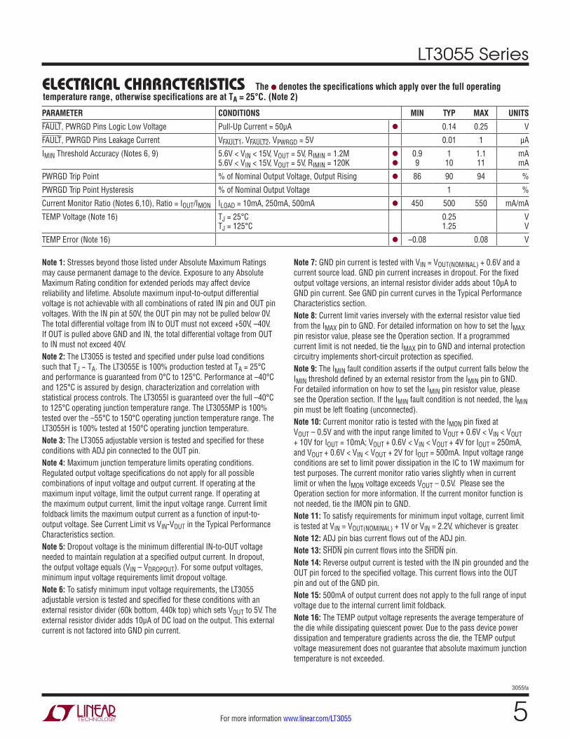
ELECTRICAL CHARACTERISTICS The l denotes the specifications which apply over the full operating temperature range, otherwise specifications are at TA = 25°C. (Note 2)
PARAMETER CONDITIONS MIN TYP MAX UNITS
Minimum Input Voltage (Note 3, 11) ILOAD = 500mA l 1.8 2.2 V
ELECTRICAL CHARACTERISTICS The l denotes the specifications which apply over the full operating temperature range, otherwise specifications are at TA = 25°C. (Note 2)
PARAMETER CONDITIONS MIN TYP MAX UNITS
FAULT, PWRGD Pins Logic Low Voltage Pull-Up Current = 50μA l 0.14 0.25 V
PWRGD Trip Point % of Nominal Output Voltage, Output Rising l 86 90 94 %
PWRGD Trip Point Hysteresis % of Nominal Output Voltage 1 %
Current Monitor Ratio (Notes 6,10), Ratio = IOUT/IMON ILOAD = 10mA, 250mA, 500mA l 450 500 550 mA/mA
TEMP Voltage (Note 16) TJ = 25°C TJ = 125°C
0.25 1.25
V V
TEMP Error (Note 16) l –0.08 0.08 V
Note 1: Stresses beyond those listed under Absolute Maximum Ratings may cause permanent damage to the device. Exposure to any Absolute Maximum Rating condition for extended periods may affect device reliability and lifetime. Absolute maximum input-to-output differential voltage is not achievable with all combinations of rated IN pin and OUT pin voltages. With the IN pin at 50V, the OUT pin may not be pulled below 0V. The total differential voltage from IN to OUT must not exceed +50V, –40V. If OUT is pulled above GND and IN, the total differential voltage from OUT to IN must not exceed 40V.Note 2: The LT3055 is tested and specified under pulse load conditions such that TJ ~ TA. The LT3055E is 100% production tested at TA = 25°C and performance is guaranteed from 0°C to 125°C. Performance at –40°C and 125°C is assured by design, characterization and correlation with statistical process controls. The LT3055I is guaranteed over the full –40°C to 125°C operating junction temperature range. The LT3055MP is 100% tested over the –55°C to 150°C operating junction temperature range. The LT3055H is 100% tested at 150°C operating junction temperature. Note 3: The LT3055 adjustable version is tested and specified for these conditions with ADJ pin connected to the OUT pin. Note 4: Maximum junction temperature limits operating conditions. Regulated output voltage specifications do not apply for all possible combinations of input voltage and output current. If operating at the maximum input voltage, limit the output current range. If operating at the maximum output current, limit the input voltage range. Current limit foldback limits the maximum output current as a function of input-to-output voltage. See Current Limit vs VIN-VOUT in the Typical Performance Characteristics section.Note 5: Dropout voltage is the minimum differential IN-to-OUT voltage needed to maintain regulation at a specified output current. In dropout, the output voltage equals (VIN – VDROPOUT). For some output voltages, minimum input voltage requirements limit dropout voltage.Note 6: To satisfy minimum input voltage requirements, the LT3055 adjustable version is tested and specified for these conditions with an external resistor divider (60k bottom, 440k top) which sets VOUT to 5V. The external resistor divider adds 10μA of DC load on the output. This external current is not factored into GND pin current.
Note 7: GND pin current is tested with VIN = VOUT(NOMINAL) + 0.6V and a current source load. GND pin current increases in dropout. For the fixed output voltage versions, an internal resistor divider adds about 10µA to GND pin current. See GND pin current curves in the Typical Performance Characteristics section.Note 8: Current limit varies inversely with the external resistor value tied from the IMAX pin to GND. For detailed information on how to set the IMAX pin resistor value, please see the Operation section. If a programmed current limit is not needed, tie the IMAX pin to GND and internal protection circuitry implements short-circuit protection as specified. Note 9: The IMIN fault condition asserts if the output current falls below the IMIN threshold defined by an external resistor from the IMIN pin to GND. For detailed information on how to set the IMIN pin resistor value, please see the Operation section. If the IMIN fault condition is not needed, the IMIN pin must be left floating (unconnected).Note 10: Current monitor ratio is tested with the IMON pin fixed at VOUT – 0.5V and with the input range limited to VOUT + 0.6V < VIN < VOUT + 10V for IOUT = 10mA; VOUT + 0.6V < VIN < VOUT + 4V for IOUT = 250mA, and VOUT + 0.6V < VIN < VOUT + 2V for IOUT = 500mA. Input voltage range conditions are set to limit power dissipation in the IC to 1W maximum for test purposes. The current monitor ratio varies slightly when in current limit or when the IMON voltage exceeds VOUT – 0.5V. Please see the Operation section for more information. If the current monitor function is not needed, tie the IMON pin to GND.Note 11: To satisfy requirements for minimum input voltage, current limit is tested at VIN = VOUT(NOMINAL) + 1V or VIN = 2.2V, whichever is greater.Note 12: ADJ pin bias current flows out of the ADJ pin.Note 13: SHDN pin current flows into the SHDN pin.Note 14: Reverse output current is tested with the IN pin grounded and the OUT pin forced to the specified voltage. This current flows into the OUT pin and out of the GND pin.Note 15: 500mA of output current does not apply to the full range of input voltage due to the internal current limit foldback.Note 16: The TEMP output voltage represents the average temperature of the die while dissipating quiescent power. Due to the pass device power dissipation and temperature gradients across the die, the TEMP output voltage measurement does not guarantee that absolute maximum junction temperature is not exceeded.
PIN FUNCTIONSIN (Pins 1, 2): Input. These pins supply power to the device. The LT3055 requires a local IN bypass capacitor if it is located more than six inches from the main input filter capacitor. In general, battery output impedance rises with frequency, so adding a bypass capacitor in battery-powered circuits is advisable. A bypass capacitor in the range of 1µF to 10µF is sufficient. See Input Capacitance and Stability in the Applications Information section for more information.
The LT3055 regulator withstands reverse voltages on the IN pins with respect to ground and the OUT pins. In the case of a reverse input, which can happen if a battery is plugged in backwards, the device acts as if there is a diode in series with its input. No reverse current flows into the regulator and no reverse voltage appears at the load.The device protects both itself and the load.
SHDN (Pin 3): Shutdown. Pulling the SHDN pin low puts the LT3055 into a low power state and turns the output off. Drive the SHDN pin with either logic or an open-collector/drain with a pull-up resistor. The resistor supplies the pull-up current to the open-collector/drain logic, normally several microamperes, and the SHDN pin current, typically less than 2μA. If unused, connect the SHDN pin to IN. The LT3055 does not function if the SHDN pin is not connected.
FAULT1 (Pin 4), FAULT2 (Pin 5): Fault Indicator Pins. FAULT1 and FAULT2 are open-collector logic pins. If the output current drops below the minimum current thresh-old, FAULT1 asserts low. If the output current exceeds the current limit threshold, FAULT2 asserts low. If the LT3055 enters thermal shutdown, both FAULT1 and FAULT2 assert low. The FAULT1 and FAULT2 pins are capable of sinking 50μA. There is no internal pull-up resistor; an external pull-up resistor must be used.
PWRGD (Pin 6): Power Good Pin. The PWRGD pin is an open-collector output that actively pulls low if the output is less than 90% of the nominal output value. The PWRGD pin is capable of sinking 50μA. There is no internal pull-up resistor, an external pull-up resistor must be used.
TEMP (Pin 7): Temperature Output. The TEMP pin outputs a voltage proportional to the average junction temperature. The pin voltage is 250mV for 25°C and has a slope of 10mV/°C.The TEMP pin output impedance is approximately 1500Ω. The TEMP pin is stable with no bypass capacitor or with a bypass capacitor with a value between 100pF and 1nF. A 100pF capacitor is recommended to improve TEMP pin power supply rejection. If not used, leave TEMP unconnected.
IMON (Pin 8): Output Current Monitor. This pin is the col-lector of a PNP current mirror that outputs 1/500th of the power PNP current. The IMON pin requires a small (22nF minimum) decoupling capacitor. In applications where the IMON pin is used in an external feedback network (current sharing, cable drop compensation, etc.) smaller bypass capacitance values may be used to ensure stability of the external feedback network. If not used, tie IMON to GND.
IMIN (Pin 9): Minimum Output Current Programming Pin. This pin is the collector of a PNP current mirror that outputs 1/2000th of the power PNP load current. This pin is also the input to the minimum output current fault com-parator. Connecting a resistor between IMIN and GND sets the minimum output current fault threshold. For detailed information on how to set the IMIN pin resistor value, please see the Operation section. A small external decoupling capacitor (10nF minimum) is required to improve IMIN PSRR. If minimum output current programming is not required, float the IMIN pin (unconnected).
IMAX (Pin 10): Precision Current Limit Programming Pin. This pin is the collector of a current mirror PNP that is 1/500th the size of the output power PNP. This pin is also the input to the current limit amplifier. Current limit threshold is set by connecting a resistor between the IMAX pin and GND. For detailed information on how to set the IMAX pin resistor value, please see the Operation section. The IMAX pin requires a 22nF decoupling capacitor to ground. If not used, tie IMAX to GND.
PIN FUNCTIONSREF/BYP (Pin 11): Bypass/Soft-Start. Connecting a capaci-tor from this pin to GND bypasses the LT3055’s reference noise and soft starts the reference. A 10nF bypass capaci-tor typically reduces output voltage noise to 25μVRMS in a 10Hz to 100kHz bandwidth. Soft-start time is directly proportional to BYP/SS capacitor value. If the LT3055 is placed in shutdown, BYP/SS is actively pulled low by an internal device to reset soft-start. If low noise or soft-start performance is not required, this pin must be left floating (unconnected). Do not drive this pin with any active cir-cuitry. Because the REF/BYP pin is the reference input to the error amplifier, stray capacitance at this point should be minimized. Special attention should be given to any stray capacitances that can couple external signals onto the REF/BYP pin producing undesirable output transients or ripple. A minimum REF/BYP capacitance of 100pF is recommended.
GND (LT3055: Pin 12, Pin 13, Exposed Pad Pin 17): Ground. The exposed pad of the DFN and MSOP pack-ages is an electrical connection to GND. To ensure proper electrical and thermal performance, solder Pin 17 to the PCB ground and tie it directly to Pins 12, 13. Connect the bottom of the output voltage setting resistor divider directly to GND (Pin 12) for optimum load regulation.
GND (LT3055-3.3, LT3055-5: Pin 12, Exposed Pad Pin 17): Ground. The exposed pad of the DFN and MSOP packages is an electrical connection to GND. To ensure proper electrical and thermal performance, solder Pin 17 to the PCB ground and tie it directly to Pin 12. Connect the bottom of the output voltage setting resistor divider directly to GND (Pin 12) for optimum load regulation.
IN
SHDN
3055 F01
RPOUT
VINSENSE
GND
LT3055-5
RP
+++LOAD
Figure 1. Kelvin Sense Connection
ADJ (LT3055: Pin 14): Adjust. This pin is the error amplifier’s inverting terminal. The typical bias current of 16nA flows out of the pin (see the ADJ pin Bias Current vs Temperature curve in the Typical Performance Characteristics section). The ADJ pin voltage is 600mV referenced to GND.
Connecting a capacitor from ADJ to OUT reduces output noise and improves transient response for output voltages greater than 600mV. See the Applications information sec-tion for calculating the value of the feedforward capacitor.
ADJ (LT3055-3.3, LT3055-5: Pin 13): Adjust. This pin is the error amplifier’s inverting terminal. The typical bias current of 16nA flows out of the pin (see the ADJ pin Bias Current vs Temperature curve in the Typical Performance Characteristics section). The ADJ pin voltage is 600mV referenced to GND.
Connecting a capacitor from ADJ to OUT reduces output noise and improves transient response for output voltages greater than 600mV. See the Applications information sec-tion for calculating the value of the feedforward capacitor.
SENSE (LT3055-3.3, LT3055-5: Pin 14): Sense. This pin is the top of the internal resistor divider network. SENSE should be connected directly to the load, as a Kelvin sense, for optimum load regulation and transient performance. Connecting this pin to the output pin, rather than directly to the load, can result in load regulation errors due to the current across the parasitic resistance of the PCB trace.
OUT (Pins 15,16): Output. These pins supply power to the load. Stability requirements demand a minimum 3.3μF ceramic output capacitor with an ESR < 1Ω to prevent oscillations. For output voltages less than 1.2V, a mini-mum 4.7µF ceramic output capacitor is required. Large load transient applications require larger output capaci-tors to limit peak voltage transients. See the Applications Information section for details on output capacitance and reverse output characteristics. Permissible output voltage range is 600mV to 40V.
The IMON pin is the collector of a PNP which mirrors the LT3055 output PNP at a ratio of 1:500 (see Block Diagram). There is additional circuitry which compensates for early voltage variation by regulating the collector of the IMON mirror PNP at the output voltage. This circuitry is active for VIMON ≤ (VOUT – 500mV). For the range where the
early voltage compensation circuit is active, calculate the output current from the simple equation:
IOUT = 500 •
VIMONRIMON
For VIMON > (VOUT-500mV), the IMON mirror PNP collec-tor is VIMON + VDSSAT (500mV at 500mA). Early voltage effects increase the IOUT to IMON ratio as VIMON increases.
OPERATIONIf the open-circuit detection function is not needed, the IMIN pin must be left floating (unconnected). A small de-coupling capacitor (10nF minimum) from IMIN to GND is required to improve IMIN pin power supply rejection and to prevent FAULT1 pin glitches. See the Typical Performance Characteristics section for additional information.
IMAX Pin Operation
The IMAX pin is the collector of a PNP which mirrors the LT3055 output PNP at a ratio of 1:500 (see Block Diagram). The IMAX pin is also the input to the precision current limit amplifier. If the output load increases to the point where it causes the IMAX pin voltage to reach 0.6V, the current limit amplifier takes control of the output regulation so that the IMAX pin regulates at 0.6V, regardless of the output voltage. The current limit threshold (ILIMIT) is set by connecting a resistor (RIMAX) from IMAX to GND:
RIMAX = 500 •
0.6VILIMIT
In cases where the IN to OUT differential voltage exceeds 10V, fold-back current limit lowers the internal current limit level, possibly causing it to override the external programmable current limit. See the Internal Current Limit vs VIN-VOUT graph in the Typical Performance Character-istics section.
The IMAX pin requires a 22nF decoupling capacitor. If the external programmable current limit is not needed, the IMAX pin must be connected to GND. The IMAX threshold is affected by power dissipation in the LT3055; it increases at a rate of approximately 0.5 percent per watt.
FAULT Pins Operation
The FAULT1 and FAULT2 pins are open-drain high voltage NMOS digital outputs. The FAULT1 pin asserts during a low current fault (open circuit). The FAULT2 pin asserts during a current limit fault (internal or externally programmed). Both FAULT1 and FAULT2 assert during thermal shutdown. There is no internal pull-up on the FAULT pins; an external pull-up resistor is required. The FAULT pins sink up to 50μA of pull-down current. Off state logic may be as high as 45V, regardless of the input voltage used.
VOUT (V)0
475
I OUT
:I IM
ON R
ATIO
(mA/
mA)
485
495
505
1 2 3 4
3055 F03a
515
525
VIN = 6VVIMON = 2.5VIOUT = 500mA (IN CURRENT LIMIT)
480
490
500
510
520
5
EARLY VOLTAGEEFFECTS
VIMON (V)0
475
I OUT
:I IM
ON R
ATIO
(mA/
mA)
485
495
505
1 2 3 4
3055 F03b
5
515
525VIN = 6VVOUT = 5VIOUT = 500mA
480
490
500
510
520
6
IMON MIRRORPNP SATURATING
EARLY VOLTAGEEFFECTS
Figure 3a. IOUT:IIMON Ratio vs VOUT
Figure 3b. IOUT:IIMON Ratio vs VIMON
In addition, if VIN – VIMON < 1V, the IMON mirror PNP saturates at high loads, causing the IOUT-to-IMON ratio to increase quickly. The IMON mirror ratio is affected by power dissipation in the LT3055; it increases at a rate of approximately 0.5 percent per watt.
Open-Circuit Detection (IMIN Pin)
The IMIN pin is the collector of a PNP which mirrors the LT3055 output PNP at a ratio of 1:2000 (see Block Diagram). The IMIN fault comparator asserts the FAULT1 pin if the IMIN pin voltage is below 0.6V. This low output current fault threshold voltage (IOPEN) is set by attaching a resistor from IMIN to GND:
STATUS FAULT1 FAULT2Open Circuit Low HighCurrent Limit High Low
Thermal Shutdown Low Low
Depending on the IMIN capacitance, BYP capacitance, and OUT capacitance, the FAULT pins may assert during start-up. Consideration should be given to masking the fault signals during start-up. The FAULT pin circuitry is inactive (not asserted) during shutdown and when the OUT pin is pulled above IN pin.
PWRGD Pin Operation
The PWRGD pin is an open-drain high voltage NMOS digital output. The PWRGD pin deasserts and becomes high impedance if the output rises above 90% of its nominal value. If the output falls below 89% of its nominal
value for more than 25μs, the PWRGD pin asserts low. The PWRGD comparator has 1% hysteresis and 25μs of deglitching. The PWRGD comparator has a dedicated reference that does not soft-start when a capacitor is added to the REF/BYP pin.
The use of a feed-forward capacitor, CFF, as shown in Fig-ure 5, can result in the ADJ pin being pulled artificially high during start- up transients, which causes the PWRGD flag to assert early. To avoid this problem, ensure that the REF/BYP capacitor is significantly larger than the feed-forward capacitor, causing REF/BYP time constant to dominate over the time constant of the resistor divider network.
Operation in Dropout
There may be some degradation of the current mirror ac-curacy for output currents less than 50mA when operating in dropout.
APPLICATIONS INFORMATIONThe LT3055 is a micropower, low noise and low dropout volt-age, 500mA linear regulator with micropower shutdown, programmable current limit, and diagnostic functions. The device supplies up to 500mA at a typical dropout voltage of 350mV and operates over a 2.2V to 45V input range.
A single external capacitor provides low noise reference performance and output soft-start functionality. For ex-ample, connecting a 10nF capacitor from the REF/BYP pin to GND lowers output noise to 25μVRMS over a 10Hz to 100kHz bandwidth. This capacitor also soft starts the reference and prevents output voltage overshoot at turn-on.
The LT3055’s quiescent current is merely 65μA but provides fast transient response with a minimum low ESR 3.3μF ceramic output capacitor. In shutdown, quiescent current is less than 1μA and the reference soft-start capacitor is reset.
The LT3055 optimizes stability and transient response with low ESR, ceramic output capacitors. The regulator does not require the addition of ESR as is common with other regulators. The LT3055 typically provides 0.1% line regulation and 0.1% load regulation. Internal protection circuitry includes reverse battery protection, reverse output protection, reverse current protection, current limit with fold-back and thermal shutdown.
This “bullet-proof” protection set makes it ideal for use in battery-powered, automotive and industrial systems.
In battery backup applications where the output is held up by a backup battery and the input is pulled to ground, the LT3055 acts like it has a diode in series with its output and prevents reverse current flow.
The adjustable LT3055 has an output voltage range of 0.6V to 40V. The output voltage is set by the ratio of two external resistors, as shown in Figure 4. The device servos the output to maintain the ADJ pin voltage at 0.6V referenced to ground. The current in R1 is then equal to 0.6V/R1, and the current in R2 is the current in R1 minus the ADJ pin bias current.
The ADJ pin bias current, 16nA at 25°C, flows from the ADJ pin through R1 to GND. Calculate the output voltage using the formula in Figure 4. The value of R1 should be no greater than 62k to provide a minimum 10μA load cur-rent so that output voltage errors, caused by the ADJ pin bias current, are minimized. Note that in shutdown, the output is turned off and the divider current is zero. Curves of ADJ Pin Voltage vs Temperature and ADJ Pin Bias Cur-rent vs Temperature appear in the Typical Performance Characteristics section.
The LT3055 is tested and specified with the ADJ pin tied to the OUT pin, yielding VOUT = 0.6V. Specifications for output voltages greater than 0.6V are proportional to the ratio of the desired output voltage to 0.6V: VOUT/0.6V. For example, load regulation for an output current change of 1mA to 500mA is 0.5mV (typical) at VOUT = 0.6V. At VOUT = 12V, load regulation is:
12V0.6V
• 0.5mV( ) = 10mV
Table 2 shows 1% resistor divider values for some common output voltages with a resistor divider current of 10μA.
The LT3055 regulator provides low output voltage noise over a 10Hz to 100kHz bandwidth while operat-ing at full load with the addition of a bypass capacitor (CREF/BYP) from the REF/BYP pin to GND. A high quality low leakage capacitor is recommended. This capacitor bypasses the internal reference of the regulator, provid-ing a low frequency noise pole for the internal reference. With the use of 10nF for CREF/BYP, output voltage noise decreases to as low as 25μVRMS when the output voltage is set for 0.6V. For higher output voltages (generated by using a feedback resistor divider), the output voltage noise gains up proportionately when using CREF/BYP.
To lower the higher output voltage noise, include a feed-forward capacitor (CFF) from VOUT to the ADJ pin. A high quality, low leakage capacitor is recommended. This capacitor bypasses the error amplifier of the regulator, providing an additional low frequency noise pole. With the use of 10nF for both CFF and CREF/BYP, output voltage noise decreases to 25μVRMS when the output voltage is set to 5V by a 10μA feedback resistor divider. If the cur-rent in the feedback resistor divider is doubled, CFF must also be doubled to achieve equivalent noise performance.
Higher values of output voltage noise can occur if care is not exercised with regard to circuit layout and testing. Crosstalk from nearby traces induces unwanted noise onto the LT3055’s output. Power supply ripple rejection
must also be considered. The LT3055 regulator does not have unlimited power supply rejection and passes a small portion of the input noise through to the output.
Using a feedforward capacitor (CFF) from VOUT to the ADJ pin has the added benefit of improving transient response for output voltages greater than 0.6V. With no feedforward capacitor, the settling time increases as the output voltage increases above 0.6V. Use the equation in Figure 5 to determine the minimum value of CFF to achieve a transient response that is similar to the 0.6V output voltage performance regardless of the chosen output volt-age (See Figure 6 and Transient Response in the Typical Performance Characteristics section).
During start-up, the internal reference soft-starts when a bypass capacitor is present. Regulator start-up time is directly proportional to the size of the bypass capacitor (See Start-Up Time vs REF/BYP Capacitor in the Typical Performance Characteristics section). The reference by-pass capacitor is actively pulled low during shutdown to reset the internal reference.
Start-up time is also affected by the presence of a feed-forward capacitor. Start-up time is directly proportional to the size of the feedforward capacitor and the output volt-age, and is inversely proportional to the feedback resistor divider current, slowing to 15ms with a 10nF feedforward capacitor and a 10μF output capacitor for an output voltage set to 5V by a 10μA feedback resistor divider.
Output Capacitance and Transient Response
The LT3055 regulator is stable with a wide range of output capacitors. The ESR of the output capacitor affects stability, most notably with small capacitors. Use a minimum output capacitor of 3.3μF with an ESR of 1Ω or less to prevent oscillations. If a feedforward capacitor is used with output voltages set for greater than 24V, use a minimum output capacitor of 10μF. The LT3055 is a micropower device and output load transient response is a function of output ca-pacitance. Larger values of output capacitance decrease the peak deviations and provide improved transient response for larger load current changes. Bypass capacitors, used to decouple individual components powered by the LT3055, increase the effective output capacitor value. For applica-tions with large load current transients, a low ESR ceramic
capacitor in parallel with a bulk tantalum capacitor often provides an optimally damped response.
Give extra consideration to the use of ceramic capacitors. Manufacturers make ceramic capacitors with a variety of dielectrics, each with different behavior across tempera-ture and applied voltage. The most common dielectrics are specified with EIA temperature characteristic codes of Z5U, Y5V, X5R and X7R. The Z5U and Y5V dielectrics provide high C-V products in a small package at low cost, but exhibit strong voltage and temperature coefficients, as shown in Figures 7 and 8. When used with a 5V regulator, a 16V 10μF Y5V capacitor can exhibit an effective value as low as 1μF to 2μF for the DC bias voltage applied, and over the operating temperature range. The X5R and X7R dielectrics yield much more stable characteristics and are more suitable for use as the output capacitor.
The X7R type works over a wider temperature range and has better temperature stability, while the X5R is less expensive and is available in higher values. Care still must be exercised when using X5R and X7R capacitors; the X5R
APPLICATIONS INFORMATION
3055 F05
IN
SHDN
OUT
ADJ
GND REF/BYP
LT3055VIN
VOUT
CREF/BYP
CFFR2
R1
COUT+
CFF ≥ 10nF10µA
• IFB _DIVIDER( )
IFB _DIVIDER = VOUTR1+R2
Figure 5. Feedforward Capacitor for Fast Transient Response
Figure 6. Transient Response vs Feedforward Capacitor
and X7R codes only specify operating temperature range and maximum capacitance change over temperature. Capacitance change due to DC bias with X5R and X7R capacitors is better than Y5V and Z5U capacitors, but can still be significant enough to drop capacitor values below appropriate levels. Capacitor DC bias characteristics tend to improve as component case size increases, but expected capacitance at operating voltage should be verified.
Voltage and temperature coefficients are not the only sources of problems. Some ceramic capacitors have a piezoelectric response. A piezoelectric device generates voltage across its terminals due to mechanical stress, similar to the way a piezoelectric accelerometer or micro-phone works. For a ceramic capacitor, the stress is induced by vibrations in the system or thermal transients. The resulting voltages produced cause appreciable amounts
APPLICATIONS INFORMATION
DC BIAS VOLTAGE (V)
CHAN
GE IN
VAL
UE (%
)
3055 F07
20
0
–20
–40
–60
–80
–1000 4 8 102 6 12 14
X5R
Y5V
16
BOTH CAPACITORS ARE 16V,1210 CASE SIZE, 10µF
TEMPERATURE (°C)–50
40
20
0
–20
–40
–60
–80
–10025 75
3055 F08
–25 0 50 100 125
Y5V
CHAN
GE IN
VAL
UE (%
) X5R
BOTH CAPACITORS ARE 16V,1210 CASE SIZE, 10µF
Figure 7. Ceramic Capacitor DC Bias Characteristics
Figure 8. Ceramic Capacitor Temperature Characteristics
Figure 9. Noise Resulting from Tapping On a Ceramic Capacitor
of noise. A ceramic capacitor produced the trace in Figure 9 in response to light tapping from a pencil. Similar vibration induced behavior can masquerade as increased output voltage noise.
Stability and Input Capacitance
Low ESR, ceramic input bypass capacitors are acceptable for applications without long input leads. However, appli-tions connecting a power supply to an LT3055 circuit’s IN and GND pins with long input wires combined with a low ESR, ceramic input capacitors are prone to voltage spikes, reliability concerns and application-specific board oscillations.
The input wire inductance found in many battery-powered applications, combined with the low ESR ceramic input capacitor, forms a high Q LC resonant tank circuit. In some instances this resonant frequency beats against the output current dependent LDO bandwidth and interferes with proper operation. Simple circuit modifications/solu-tions are then required. This behavior is not indicative of LT3055 instability, but is a common ceramic input bypass capacitor application issue.
The self-inductance, or isolated inductance, of a wire is directly proportional to its length. Wire diameter is not a major factor on its self-inductance. For example, the self-inductance of a 2-AWG isolated wire (diameter = 0.26") is about half the self-inductance of a 30-AWG wire (diameter = 0.01"). One foot of 30-AWG wire has approxi-mately 465nH of self-inductance.
APPLICATIONS INFORMATIONTwo methods can reduce wire self-inductance. One method divides the current flowing towards the LT3055 between two parallel conductors. In this case, the farther apart the wires are from each other, the more the self-inductance is reduced; up to a 50% reduction when placed a few inches apart. Splitting the wires connects two equal inductors in parallel, but placing them in close proximity creates mutual inductance adding to the self-inductance. The second and most effective way to reduce overall inductance is to place both forward and return current conductors (the input and GND wires) in very close proximity. Two 30-AWG wires separated by only 0.02”, used as forward- and return-current conductors, reduce the overall self-inductance to approximately one-fifth that of a single isolated wire.
If a battery, mounted in close proximity, powers the LT3055, a 10µF input capacitor suffices for stability. However, if a distant supply powers the LT3055, use a larger value input capacitor. Use a rough guideline of 1µF (in addition to the 10µF minimum) per 8 inches of wire length. The minimum input capacitance needed to stabilize the application also varies with power supply output impedance variations. Placing additional capacitance on the LT3055’s output also helps. However, this requires an order of magnitude more capacitance in comparison with additional LT3055 input bypassing. Series resistance between the supply and the LT3055 input also helps stabilize the application; as little
as 0.1Ω to 0.5Ω suffices. This impedance dampens the LC tank circuit at the expense of dropout voltage. A better alternative is to use higher ESR tantalum or electrolytic ca-pacitors at the LT3055 input in place of ceramic capacitors.
Paralleling Devices
Higher output current is obtained by paralleling multiple LT3055 together. Tie the individual OUT pins together and tie the individual IN pins together. An external NPN or NMOS current mirror is used in combination with the LT3055 IMON pins to create a simple amplifier. This ampli-fier injects current into or out of the feedback divider of the slave LT3055 in order to ensure that the IMON currents from each LT3055 are equal.
In Figure 10, this is implemented using inexpensive 2N3904 NPN devices. Precision 1k resistors provide 1V emitter degeneration at full load to guarantee good current mirror matching. The feedback resistors of the slave LT3055 are split into sections to ensure adequate headroom for the slave 2N3904. A 1nF capacitor added to the IMON pin of the slave device frequency compensates the feedback loop.
This circuit architecture is scalable to as many LT3055s as are needed simply by extending the current mirror and adding slave LT3055 devices.
Spreading the devices on the PC board also spreads the heat. Series input resistors can further spread the heat if the input-to-output differential is high.
Overload Recovery
Like many IC power regulators, the LT3055 has safe oper-ating area protection. The safe area protection decreases current limit as input-to-output voltage increases, and keeps the power transistor inside a safe operating region for all values of input-to-output voltage. The LT3055 pro-vides some output current at all values of input-to-output voltage up to the device breakdown.
When power is first applied, the input voltage rises and the output follows the input; allowing the regulator to start-up into very heavy loads. During start-up, as the input voltage is rising, the input-to-output voltage differential is small, al-lowing the regulator to supply large output currents. With a high input voltage, a problem can occur wherein the removal of an output short will not allow the output to recover. Other regulators, such as the LT1083/LT1084/ LT1085 family and LT1764A also exhibit this phenomenon, so it is not unique to the LT3055. The problem occurs with a heavy output load when the input voltage is high and the output voltage is low. Common situations are immediately after the removal of a short circuit or if the shutdown pin is pulled high after the input voltage is already turned on. The load line intersects the output current curve at two points. If this happens, there are two stable output operating points for the regulator. With this double intersection, the input power supply needs to be cycled down to zero and back up again to recover the output.
Thermal Considerations
The LT3055’s maximum rated junction temperature of 125°C (E-, I-grades) or 150°C (MP-, H-grades) limits its power handling capability. Two components comprise the power dissipated by the device:
1. Output current multiplied by the input/output voltage differenvl:
IOUT • (VIN – VOUT), and
2. GND pin current multiplied by the input voltage:
IGND • VIN
GND pin current is determined using the GND Pin Current curves in the Typical Performance Characteristics section.Power dissipation equals the sum of the two components listed above.
The LT3055 regulator has internal thermal limiting that protects the device during overload conditions. For con-tinuous normal conditions, do not exceed the maximum junction temperature of 125°C (E-, I-grades) or 150°C (MP-, H-grades). Carefully consider all sources of thermal resistance from junction-to-ambient including other heat sources mounted in proximity to the LT3055.
The undersides of the LT3055 DFN and MSE packages have exposed metal from the lead frame to the die attachment. These packages allow heat to directly transfer from the die junction to the printed circuit board metal to control maximum operating junction temperature. The dual-in-line pin arrangement allows metal to extend beyond the ends of the package on the topside (component side) of a PCB. Connect this metal to GND on the PCB. The multiple IN and OUT pins of the LT3055 also assist in spreading heat to the PCB.
For surface mount devices, heat sinking is accomplished by using the heat spreading capabilities of the PC board and its copper traces. Copper board stiffeners and plated through-holes also can spread the heat generated by power devices.
Tables 3 and 4 list thermal resistance as a function of copper area in a fixed board size. All measurements were taken in still air on a 4-layer FR-4 board with 1oz solid internal planes, and 2oz external trace planes with a total board thickness of 1.6mm. For further information on thermal resistance and using thermal information, refer to JEDEC standard JESD51, notably JESD51-12.
APPLICATIONS INFORMATION
Table 3. MSOP Measured Thermal ResistanceCOPPER AREA
Example: Given an output voltage of 5V, an input voltage range of 12V ±5%, a maximum output current range of 75mA and a maximum ambient temperature of 85°C, what is the maximum junction temperature?
The power dissipated by the device equals:
IOUT(MAX) • (VIN(MAX) – VOUT) + IGND • VIN(MAX)
where:
IOUT(MAX) = 75mA
VIN(MAX) = 12.6V
IGND at (IOUT = 75mA, VIN = 12V) = 3.5mA
So:
P = 75mA • (12.6V – 5V) + 3.5mA • 12.6V = 0.614W
Using a DFN package, the thermal resistance ranges from 36°C/W to 40°C/W depending on the copper area. So the junction temperature rise above ambient approximately equals:
0.614W • 40°C/W = 24.6°C
The maximum junction temperature equals the maximum ambient temperature plus the maximum junction tempera-ture rise above ambient or:
TJMAX = 85°C + 24.6°C = 110°C
Protection Features
The LT3055 incorporates several protection features that make it ideal for use in battery-powered circuits. In ad-dition to the normal protection features associated with monolithic regulators, such as current limiting and thermal
limiting, the device also protects against reverse input voltages, reverse output voltages and reverse output-to-input voltages.
Current limit protection and thermal overload protection protect the device against current overload conditions at the output of the device. For normal operation, do not exceed a junction temperature of 125°C (E-, I-grades) or 150°C (MP-, H-grades).
The LT3055 IN pin withstands reverse voltages of 50V. The device limits current flow to less than 1μA (typically less than 25nA) and no negative voltage appears at OUT. The device protects both itself and the load against batteries that are plugged in backwards.
The LT3055 incurs no damage if its output is pulled below ground. If the input is left open circuit or grounded, the output can be pulled below ground by 50V. No current flows through the pass transistor from the output. However, current flows in (but is limited by) the feedback resistor divider that sets the output voltage. Current flows from the bottom resistor in the divider and from the ADJ pin’s internal clamp through the top resistor in the divider to the external circuitry pulling OUT below ground. If the input is powered by a voltage source, the output sources current equal to its current limit capability and the LT3055 protects itself by thermal limiting. In this case, grounding the SHDN pin turns off the device and stops the output from sourcing current.
PACKAGE DESCRIPTIONPlease refer to http://www.linear.com/designtools/packaging/ for the most recent package drawings.
MSOP (MSE16) 0213 REV F
0.53 ±0.152(.021 ±.006)
SEATINGPLANE
0.18(.007)
1.10(.043)MAX
0.17 – 0.27(.007 – .011)
TYP
0.86(.034)REF
0.50(.0197)
BSC
16
16151413121110
1 2 3 4 5 6 7 8
9
9
1 8
NOTE:1. DIMENSIONS IN MILLIMETER/(INCH)2. DRAWING NOT TO SCALE3. DIMENSION DOES NOT INCLUDE MOLD FLASH, PROTRUSIONS OR GATE BURRS. MOLD FLASH, PROTRUSIONS OR GATE BURRS SHALL NOT EXCEED 0.152mm (.006") PER SIDE4. DIMENSION DOES NOT INCLUDE INTERLEAD FLASH OR PROTRUSIONS. INTERLEAD FLASH OR PROTRUSIONS SHALL NOT EXCEED 0.152mm (.006") PER SIDE5. LEAD COPLANARITY (BOTTOM OF LEADS AFTER FORMING) SHALL BE 0.102mm (.004") MAX6. EXPOSED PAD DIMENSION DOES INCLUDE MOLD FLASH. MOLD FLASH ON E-PAD SHALL NOT EXCEED 0.254mm (.010") PER SIDE.
PACKAGE DESCRIPTIONPlease refer to http://www.linear.com/designtools/packaging/ for the most recent package drawings.
3.00 ±0.10(2 SIDES)
4.00 ±0.10(2 SIDES)
NOTE:1. DRAWING PROPOSED TO BE MADE VARIATION OF VERSION (WGED-3) IN JEDEC PACKAGE OUTLINE MO-2292. DRAWING NOT TO SCALE 3. ALL DIMENSIONS ARE IN MILLIMETERS4. DIMENSIONS OF EXPOSED PAD ON BOTTOM OF PACKAGE DO NOT INCLUDE MOLD FLASH. MOLD FLASH, IF PRESENT, SHALL NOT EXCEED 0.15mm ON ANY SIDE5. EXPOSED PAD SHALL BE SOLDER PLATED6. SHADED AREA IS ONLY A REFERENCE FOR PIN 1 LOCATION ON THE TOP AND BOTTOM OF PACKAGE
0.40 ±0.10
BOTTOM VIEW—EXPOSED PAD
1.70 ±0.10
0.75 ±0.05
R = 0.115TYP
R = 0.05TYP
3.15 REF
1.70 ±0.05
18
169
PIN 1TOP MARK
(SEE NOTE 6)
0.200 REF
0.00 – 0.05
(DE16) DFN 0806 REV Ø
PIN 1 NOTCHR = 0.20 OR0.35 × 45°CHAMFER
3.15 REF
RECOMMENDED SOLDER PAD PITCH AND DIMENSIONSAPPLY SOLDER MASK TO AREAS THAT ARE NOT SOLDERED
Information furnished by Linear Technology Corporation is believed to be accurate and reliable. However, no responsibility is assumed for its use. Linear Technology Corporation makes no representa-tion that the interconnection of its circuits as described herein will not infringe on existing patent rights.
REVISION HISTORYREV DATE DESCRIPTION PAGE NUMBER
A 7/14 Modified Minimum VIN to 1.8VAdded 3.3V and 5V options, related specs, Typical Performance Characteristics and Pin FunctionsAdded specification for absolute maximum SENSE pin voltageModified Pinouts to accommodate new fixed voltage optionsModified Note 7Modified PWRGD applications section
LT1965 1.1A, Low Noise, Low Dropout Linear Regulator
290mV Dropout Voltage, Low Noise: 40μVRMS, VIN: 1.8V to 20V, VOUT: 1.2V to 19.5V, Stable with Ceramic Capacitors, TO-220, DDPak, MSOP and 3mm × 3mm DFN Packages
LT3008 20mA, 45V, 3µA IQ Micropower LDO 300mV Dropout Voltage, Low IQ = 3μA, VIN: 2.0V to 45V, VOUT: 0.6V to 39.5V, ThinSOT and 2mm × 2mm DFN-6 Packages
LT3009 20mA, 3µA IQ Micropower LDO 280mV Dropout Voltage, Low IQ = 3μA, VIN: 1.6V to 20V, 2mm × 2mm DFN-6 and SC-70 Packages
LT3010 50mA, High Voltage, Micropower LDO VIN: 3V to 80V, VOUT: 1.275V to 60V, VDO = 0.3V, IQ = 30μA, ISD < 1μA, Low Noise: <100μVRMSP-P, Stable with 1μF Output Capacitor, Exposed MS8 Package
LT3011 50mA, High Voltage, Micropower LDO with PWRGD
VIN: 3V to 80V, VOUT: 1.275V to 60V, VDO = 0.3V, IQ = 46μA, ISD < 1μA, Low Noise: <100μVRMS, PowerGood, Stable with 1μF Output Capacitor, 3mm × 3mm DFN-10 and Exposed MS12E Packages
LT3012 250mA, 4V to 80V, Low Dropout Micropower Linear Regulator
VIN: 4V to 80V, VOUT: 1.24V to 60V, VDO = 0.4V, IQ = 40μA, ISD < 1μA, TSSOP-16E and 4mm × 3mm DFN-12 Packages
LT3013 250mA, 4V to 80V, Low Dropout Micropower Linear Regulator with PWRGD
VIN: 4V to 80V, VOUT: 1.24V to 60V, VDO = 0.4V, IQ = 65μA, ISD < 1μA, PowerGood Feature, TSSOP-16E and 4mm × 3mm DFN-12 Packages
LT3014/LT3014HV 20mA, 3V to 80V, Low Dropout Micropower Linear Regulator
VIN: 3V to 80V (100V for 2ms, LT3014HV Version), VOUT: 1.22V to 60V, VDO = 0.35V, IQ = 7μA, ISD < 1μA, ThinSOT and 3mm × 3mm DFN-8 Packages
LT3080/LT3080-1 1.1A, Parallelable, Low Noise, Low Dropout Linear Regulator
300mV Dropout Voltage (2-Supply 0peration), Low Noise: 40μVRMS, VIN: 1.2V to 36V, VOUT: 0V to 35.7V, Current-Based Reference with 1-Resistor VOUT Set, Directly Parallelable (No Op Amp Required), Stable with Ceramic Capacitors, TO-220, SOT-223, MSOP and 3mm × 3mm DFN Packages, LT3080-1 Version Has Integrated Internal Ballast Resistor
LT3050 100mA LDO with Diagnostics and Precision Current Limit
340mV Dropout Voltage, Low Noise: 20μVRMS, VIN: 1.8V to 45V, DFN and MSOP Packages
LT3060 100mA, Low Noise LDO with Soft-Start 300mV Dropout Voltage, Low Noise: 20μVRMS, VIN: 1.8V to 45V, DFN Package