1 ACADEMIC REGULATIONS, COURSE STRUCTURE AND DETAILED SYLLABUS UNDER CHOICE BASED CREDIT SYSTEM (CBCS) Effective from the Academic Year 2015-16 M. Tech. Two Year Degree Course (MR-15 Regulations) in VLSI SYSTEM DESIGN (VLSI SD) Department of Electronics & Communication Engineering MALLA REDDY ENGINEERING COLLEGE (Autonomous) (An Autonomous Institution approved by UGC and affiliated to JNTUH, Approved by AICTE & Accredited by NAAC with ‘A’ Grade and NBA & Recipient of World Bank Assistance under TEQIP Phase – II, S.C 1.1) Maisammaguda, Dhulapally (Post & Via Kompally), Secunderabad-500 100 www.mrec.ac.in E-mail: [email protected]
Transcript
1
ACADEMIC REGULATIONS, COURSE STRUCTURE
AND DETAILED SYLLABUS UNDER
CHOICE BASED CREDIT SYSTEM (CBCS) Effective from the Academic Year 2015-16
M. Tech. Two Year Degree Course
(MR-15 Regulations) in
VLSI SYSTEM DESIGN (VLSI SD) Department of Electronics & Communication Engineering
MALLA REDDY ENGINEERING COLLEGE (Autonomous)
(An Autonomous Institution approved by UGC and affiliated to JNTUH, Approved by AICTE & Accredited by NAAC with ‘A’ Grade and NBA & Recipient of World Bank Assistance under TEQIP Phase – II, S.C 1.1)
MALLA REDDY ENGINEERING COLLEGE (AUTONOMOUS) MR 15– ACADEMIC REGULATIONS (CBCS) FOR M. Tech. (REGULAR) DEGREE
PROGRAMME Applicable for the students of M. Tech. (Regular) programme from the Academic Year 2015-16 and onwards The M. Tech. Degree of Jawaharlal Nehru Technological University Hyderabad shall be conferred on candidates who are admitted to the programme and who fulfill all the requirements for the award of the Degree.
INSTITUTION VISION
A Culture of excellence , the hallmark of MREC as world class education center to impart Technical Knowledge in an ambience of humanity, wisdom, intellect, creativity with ground breaking discovery, in order to nurture the students to become Globally competent committed professionals with high discipline, compassion and ethical values.
INSTITUTION MISSION Commitment to progress in mining new knowledge by adopting cutting edge technology to promote academic growth by offering state of art Under graduate and Post graduate programmes based on well-versed perceptions of Global areas of specialization to serve the Nation with Advanced Technical knowledge.
DEPARTMENT VISION
With a vision to develop innovative, globally competent and quality electronic engineers by imparting state of art technology to foster a climate of high professionalism, ethical values, excellence and devotion.
DEPARTMENT MISSION
To enrich the knowledge of students through quality and value based education. To organize various effective training programs in order to compete the advanced
technology. To produce employable under graduates and post graduates.
PROGRAMME EDUCATIONAL OBJECTIVES (PEOs)
PEO1: To provide the post graduate students with an advanced technical knowledge in the area of VLSI Design, so as to make them to design, analyze and create the product relevant to the course. PEO2: To train the PG students in the field of VLSI and make themselves as Research & Development engineers, industry ready with a focus on effective communication skills, team working and multidisciplinary approach. PEO3: To continue in inducing & Practicing professional ethics, honest practices to make them responsible towards the society collectively.
3
PROGRAMME OUTCOMES (POs)
PO1: PG students acquired specialized and in depth knowledge in the areas of VLSI System Design. PO2: PG Students can demonstrate their ability in analyzing the complex and critical engineering problems in their field, apart from solving the subject problems.
PO3: PG Students can demonstrate their ability to think and work independently, with minimum or no supervision, and able to provide various solutions, by due considering the importance level of the technical requirement and associated issues. PO4: PG Students can have the opportunity of working in Research & Development environment, in government organizations, and also able to develop intellectual property, patents etc., PO5: PG Students can have the opportunity to work in various industry standard tools like, Cadence, Xilinx, Altera, MicroWind and Microsoft Visual C++ 6.0 etc, which enables them industry ready, which in turn opens up and enhances the career opportunities. PO6: PG Students can become, entrepreneurs, transforming their ideas into a product and systems to benefit the society, and empower themselves socially responsible. PO7: PG Students are capable enough to write the technical reports, specifications and documenting the standards, which was imparted to them through training on communication skills, particularly verbal and written. PO8: PG Students can work in multi cultural environment using their communication skills, and builds the interpersonal relationship in a team environment, capable of managing the team to achieve the goal of the project, and support the business and service motives of the organization. PO9: PG Students can opt for higher education, particularly research in the field of VLSI System Design. Update the technical knowledge by involving in continuous learning process, being a member of profession body through research publications and in turn contribute back to the technical community. PO10: Students can apply ethical and honest practices, to commit to the professional ethics expected from them and responsible towards the society.
PO11: Students can understand the impact of electronics products on to the global environmental perspective and demonstrate their skills and knowledge for sustained development.
4
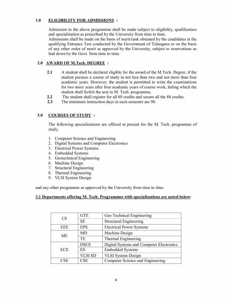
1.0 ELIGIBILITY FOR ADMISSIONS :
Admission to the above programme shall be made subject to eligibility, qualification and specialization as prescribed by the University from time to time. Admissions shall be made on the basis of merit/rank obtained by the candidates at the qualifying Entrance Test conducted by the Government of Telangana or on the basis of any other order of merit as approved by the University, subject to reservations as laid down by the Govt. from time to time.
2.0 AWARD OF M.Tech. DEGREE :
2.1 A student shall be declared eligible for the award of the M.Tech. Degree, if the
student pursues a course of study in not less than two and not more than four academic years. However, the student is permitted to write the examinations for two more years after four academic years of course work, failing which the student shall forfeit the seat in M. Tech. programme.
2.2 The student shall register for all 88 credits and secure all the 88 credits. 2.3 The minimum instruction days in each semester are 90.
3.0 COURSES OF STUDY :
The following specializations are offered at present for the M. Tech. programme of study.
1. Computer Science and Engineering 2. Digital Systems and Computer Electronics 3. Electrical Power Systems 4. Embedded Systems 5. Geotechnical Engineering 6. Machine Design 7. Structural Engineering 8. Thermal Engineering 9. VLSI System Design
and any other programme as approved by the University from time to time.
3.1 Departments offering M. Tech. Programmes with specializations are noted below:
CE GTE Geo Technical Engineering SE Structural Engineering
EEE EPS Electrical Power Systems
ME MD Machine Design TE Thermal Engineering
ECE DSCE Digital Systems and Computer Electronics ES Embedded Systems VLSI SD VLSI System Design
CSE CSE Computer Science and Engineering
5
4 COURSE REGISTRATION :
4.1 A ‘Faculty Advisor or Counselor’ shall be assigned to each student, who will advise him on the Post Graduate Programme (PGP), its Course Structure and Curriculum, Choice/Option for Subjects/ Courses, based on his competence, progress, pre-requisites and interest.
4.2 Academic Section of the College invites ‘Registration Forms’ from students
within 15 days from the commencement of class work for the first semester through ‘ON-LINE SUBMISSIONS’, ensuring ‘DATE and TIME Stamping’. The ON-LINE Registration Requests for any ‘SUBSEQUENT SEMESTER’ shall be completed BEFORE the commencement of SEEs (Semester End Examinations) of the ‘CURRENT SEMESTER’.
4.3 A Student can apply for ON-LINE Registration, ONLY AFTER obtaining the
‘WRITTEN APPROVAL’ from the Faculty Advisor, which should be submitted to the College Academic Section through the Head of Department (a copy of it being retained with Head of Department, Faculty Advisor and the Student).
4.4 If the Student submits ambiguous choices or multiple options or erroneous
entries during ON-LINE Registration for the Subject(s) / Course(s) under a given/ specified Course Group/ Category as listed in the Course Structure, only the first mentioned Subject/ Course in that Category will be taken into consideration.
4.5 Subject/ Course Options exercised through ON-LINE Registration are final
and CANNOT be changed, nor can they be inter-changed; further, alternate choices will also not be considered. However, if the Subject/ Course that has already been listed for Registration (by the Head of Department) in a Semester could not be offered due to any unforeseen or unexpected reasons, then the Student shall be allowed to have alternate choice - either for a new Subject (subject to offering of such a Subject), or for another existing Subject (subject to availability of seats), which may be considered. Such alternate arrangements will be made by the Head of Department, with due notification and time-framed schedule, within the FIRST WEEK from the commencement of Class-work for that Semester.
5 ATTENDANCE :
The programmes are offered on a unit basis with each subject/course being considered as a unit.
5.1 Attendance in all classes (Lectures/Laboratories etc.) is compulsory. The
minimum required attendance in each theory / Laboratory etc. is 75% including the days of attendance in sports, games, NCC and NSS activities for appearing for the Semester End examination (SEE). A student shall not be permitted to appear for the Semester End Examinations (SEE) if his attendance is less than 75%.
5.2 Condonation of shortage of attendance in each subject up to 10% (65% and above and below 75%) in each semester shall be granted by the College Academic Committee (CAC).
5.3 Shortage of Attendance below 65% in each subject shall not be condoned.
6
5.4 Students whose shortage of attendance is not condoned in any subject are not eligible to write their end Semester End Examination of that subject and their registration shall stand cancelled.
5.5 A fee prescribed by the CAC, shall be payable towards Condonation of shortage of attendance.
5.6 A Candidate shall put in a minimum required attendance in atleast three (3) theory subjects in I semester for promoting to II Semester. In order to qualify for the award of the M.Tech. Degree, the candidate shall complete all the academic requirements of the subjects, as per the course structure.
5.7 A student shall not be promoted to the next semester unless the student
satisfies the attendance requirement of the present Semester, as applicable. The student may seek readmission into that semester when offered next. If any candidate fulfills the attendance requirement in the present semester, the student shall not be eligible for readmission into the same class.
6 EVALUATION - DISTRIBUTION AND WEIGHTAGE OF MARKS: :
The performance of the candidate in each semester shall be evaluated subject-wise, with a maximum of 100 marks for theory and 100 marks for practicals, on the basis of Continuous Internal Evaluation and Semester End Examinations. For all Subjects/ Courses, the distribution shall be 40 marks for CIE, and 60 marks for the SEE
6.1 Theory Courses : 6.1.1 Continuous Internal Evaluation (CIE): The CIE consists of two Assignments each of 05 marks and two mid-term examinations each of 35 marks. The CIE shall be finalized based on the 70% of the best performed and 30% of the other performance.The first mid-term examination shall be conducted for the first 50% of the syllabus, and the second mid-term examination shall be conducted for the remaining 50% of the syllabus. First Assignment should be submitted before the conduct of the first mid-term examinations, and the Second Assignment should be submitted before the conduct of the second midterm examinations. The Assignments shall be as specified by the concerned subject teacher.. Each mid-term examination shall be conducted for a total duration of 120 minutes, for 35 marks.
The division of marks for CIE is as given below:
Mid – Term Examination Part Type of Questions No. of
questions Marks per question
Total
Part A Multiple-choice questions 10 0.5 05 Fill-in the blanks 10 0.5 05 Sub-Total 10
Part B Compulsory questions 5 2 10
Part C Choice questions (3 out of 5)
3 5 15
Mid-Term Exam Total 35 Assignment 05
Grand Total 40
7
6.1.2 Semester End Examination (SEE): The division of marks for SEE is as given below:
Semester End Examination
Part Type of Questions
No. of questions to be
answered
Marks per question Total
Part A
Compulsory Questions (One from each module)
5 4 20
Part B
Choice Questions (5 out of 8) (Minimum one from each module)
5 8 40
Grand Total 60 6.2 Practical Courses: 6.2.1 Continuous Internal Evaluation (CIE):
There will be CIE for 40 marks, shall be awarded with a distribution of 20 marks for day-to-day performance and timely submission of lab records, 5 marks for viva-voce, 15 marks for internal lab exam (best out of two exams).
6.2.2 Semester End Examination (SEE): There will be SEE for 60 marks, shall be awarded with a distribution of 20 marks for write-up on the given experiment, 20 marks for proficiency in the exam, 10 marks for results and 10 marks for viva-voce. For conducting SEE, one internal examiner and one external examiner will be appointed by the Chief Controller of Examinations of the College. The external examiner should be selected from outside the College among the autonomous/reputed institutions, from a panel of three examiners submitted by the concerned Head of the Department.
6.3 Seminar:
There shall be two seminar presentations during I semester and II semester. For seminar, a student under the supervision of a faculty member, shall collect the literature on a topic and critically review the literature and submit it to the department in a report form and shall make an oral presentation before the Departmental Academic Committee consisting of Head of the Department, Supervisor and two other senior faculty members of the department. For each Seminar there will be only internal evaluation of 100 marks with a distribution of 30 marks for the report, 50 marks for presentation and 20 marks for the queries. A candidate has to secure a minimum of 50% of marks to be declared successful. If the student fails to fulfill minimum marks, the student has to reappear during the supplementary examinations.
6.4 Comprehensive Viva-Voce:
There shall be a Comprehensive Viva-Voce in III Semester. The Comprehensive Viva-Voce is intended to assess the students’ understanding of various subjects studied during the M. Tech. course of study. The Head of
8
the Department shall be associated with the conduct of the Comprehensive Viva-Voce through a Committee. The Committee consists of the Head of the Department, one senior faculty member and an external examiner. The external examiner shall be appointed by the Chief Controller of Examinations from a panel of three examiners submitted by the concerned Head of the Department. There are no internal marks for the Comprehensive Viva-Voce and evaluates for maximum of 100 marks. A candidate has to secure a minimum of 50% of marks to be declared successful. If the student fails to fulfill minimum marks, the student has to reappear during the supplementary examinations.
6.5. General: A candidate shall be deemed to have secured the minimum
academic requirement in a subject if he secures a minimum of 40% of marks in the Semester End Examination and a minimum of 50% of the total marks in the Semester End Examination and Continuous Internal Evaluation taken together. In case the candidate does not secure the minimum academic requirement in any subject he has to reappear for the Semester End Examination in that subject. A candidate shall be given one chance to re-register for the subject if the internal marks secured by the candidate are less than 50% and failed in that subject. This is allowed for a maximum of three subjects and should register within two weeks of commencement of that semester class work. In such a case, the candidate must re-register for the subjects and secure the required minimum attendance. The candidate’s attendance in the re-registered subject(s) shall be calculated separately to decide upon the eligibility for writing the Semester End Examination in those subjects. In the event of the student taking another chance, the student’s Continuous Internal Evaluation (CIE) marks and Semester End Examination (SEE) marks obtained in the previous attempt stands cancelled.
7 EXAMINATIONS AND ASSESSMENT - THE GRADING SYSTEM :
7.1 Marks will be awarded to indicate the performance of each student in each Theory Subject, or Lab / Practicals, or Seminar, or Project, etc., based on the % marks obtained in CIE + SEE (Continuous Internal Evaluation + Semester End Examination, both taken together) as specified in Item 6 above, and a corresponding Letter Grade shall be given.
7.2 As a measure of the student’s performance, a 10-point Absolute Grading
System using the following Letter Grades (UGC Guidelines) and corresponding percentage of marks shall be followed:
% of Marks Secured (Class Intervals)
Grade Points
Letter Grade (UGC Guidelines)
≥ 80% 10 O (Outstanding) ≥ 70% to < 80% 9 A+ (Excellent) ≥ 60% to < 70% 8 A (Very Good) ≥ 55% to < 60% 7 B+ (Good) ≥ 50% to < 55% 6 B (Above Average)
< 50% 0 F (Fail) Absent Ab Ab
9
7.3 A student obtaining F Grade in any Subject shall be considered ‘failed’ and is
be required to reappear as ‘Supplementary Candidate’ in the Semester End Examination (SEE), as and when conducted. In such cases, his Internal Marks (CIE Marks) in those Subjects will remain the same as those he obtained earlier.
7.4 A student not appeared for examination then ‘Ab’ Grade will be allocated in
any Subject shall be considered ‘failed’ and will be required to reappear as ‘Supplementary Candidate’ in the Semester End Examination (SEE), as and when conducted.
7.5 A Letter Grade does not imply any specific Marks percentage and it will be
the range of marks percentage.
7.6 In general, a student shall not be permitted to repeat any Subject/ Course (s) only for the sake of ‘Grade Improvement’ or ‘SGPA/ CGPA Improvement’.
7.7 A student earns Grade Point (GP) in each Subject/ Course, on the basis of the
Letter Grade obtained by him in that Subject/ Course. The corresponding ‘Credit Points’ (CP) is computed by multiplying the Grade Point with Credits for that particular Subject/ Course. Credit Points (CP) = Grade Point (GP) x Credits …. For a Course
7.8 The Student passes the Subject/ Course only when he gets GP ≥ 6(B Grade or above).
7.9 The Semester Grade Point Average (SGPA) is calculated by dividing the Sum of Credit Points (∑CP) secured from ALL Subjects/ Courses registered in a Semester, by the Total Number of Credits registered during that Semester. SGPA is rounded off to TWO Decimal Places. SGPA is thus computed as: SGPA = ∑ C G / ∑ C … For each Semester where ‘i’ is the Subject indicator index (takes into account all Subjects in a Semester), ‘N’is the no. of Subjects ‘REGISTERED’ for the Semester (as specifically required and listed under the Course Structure of the parent Department), Ci is the no. of Credits allotted to the ith Subject, and G represents the Grade Points (GP) corresponding to the Letter Grade awarded for that ith Subject.
7.10 The Cumulative Grade Point Average (CGPA) is a measure of the overall cumulative performance of a student over all Semesters considered for registration. The CGPA is the ratio of the Total Credit Points secured by a student in ALL registered Courses in ALL Semesters, and the Total Number of Credits registered in ALL the Semesters. CGPA is rounded off to TWO Decimal Places. CGPA is thus computed from the II Semester onwards, at the end of each Semester, as per the formula CGPA = ∑ C G / ∑ C … for all S semesters registered (i.e., upto and inclusive of S semesters, S ≥ 2) where ‘M’ is the TOTAL no. of Subjects (as specifically required and listed under the Course Structure of the parent Department) the Student has
10
‘REGISTERED’ from the 1stSemester onwards upto and inclusive of the Semester S ( obviously M > N ), ‘j’ is the Subject indicator index (takes into account all Subjects from 1 to S Semesters), Cj is the no. of Credits allotted to the jth Subject, and Gj represents the Grade Points (GP)corresponding to the Letter Grade awarded for that jth Subject. After registration and completion of I Semester however, the SGPA of that Semester itself may be taken as the CGPA, as there are no cumulative effects.
7.11 For Calculations listed in Item 7.6 – 7.10, performance in failed Subjects/ Courses (securing F Grade) will also be taken into account, and the Credits of such Subjects/Courses will also be included in the multiplications and summations.
8. EVALUATION OF PROJECT/DISSERTATION WORK :
Every candidate shall be required to submit a thesis or dissertation on a topic approved by the Project Review Committee. 8.1 A Project Review Committee (PRC) shall be constituted with Head of the
Department as Chairperson, Project Supervisor and one senior faculty member of the Departments offering the M. Tech. programme.
8.2 Registration of Project Work: A candidate is permitted to register for the
project work after satisfying the attendance requirement of all the subjects, both theory and practical.
8.3 After satisfying 8.2, a candidate has to submit, in consultation with his
Project Supervisor, the title, objective and plan of action of his project work to the PRC for approval. Only after obtaining the approval of the PRC the student can initiate the Project work.
8.4 If a candidate wishes to change his supervisor or topic of the project, he can
do so with the approval of the PRC. However, the PRC shall examine whether or not the change of topic/supervisor leads to a major change of his initial plans of project proposal. If yes, his date of registration for the project work starts from the date of change of Supervisor or topic as the case may be.
8.5 A candidate shall submit his project status report in two stages at least with a
gap of 3 months between them. 8.6 The work on the project shall be initiated at the beginning of the III Semester
and the duration of the project is two semesters. A candidate is permitted to submit Project Thesis only after successful completion of all theory and practical courses with the approval of PRC not earlier than 40 weeks from the date of registration of the project work. For the approval of PRC the candidate shall submit the draft copy of thesis to the Head of the Department and make an oral presentation before the PRC. Note: The project supervisor/guide has to ensure that the student has to publish a minimum of one paper related to the thesis in a National/International Conference/Journal.
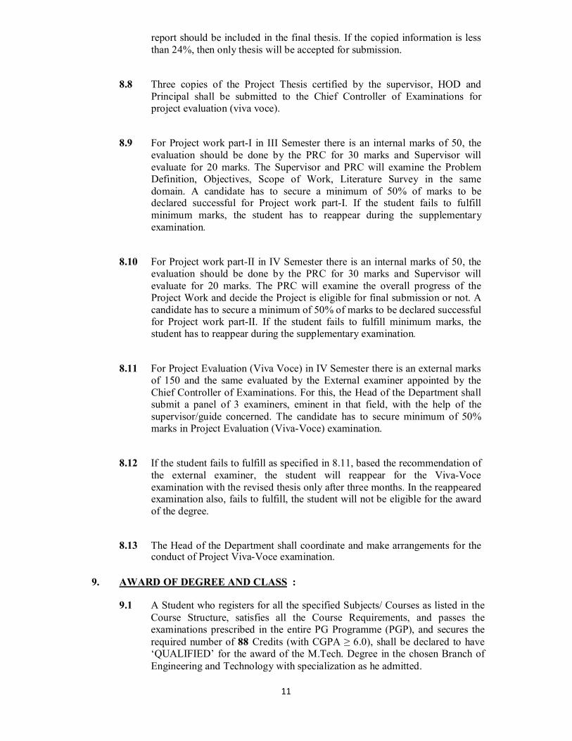
8.7 For the final approval by the PRC, the soft copy of the thesis should be submitted for ANTI-PLAGIARISM for the quality check and the plagiarism
11
report should be included in the final thesis. If the copied information is less than 24%, then only thesis will be accepted for submission.
8.8 Three copies of the Project Thesis certified by the supervisor, HOD and Principal shall be submitted to the Chief Controller of Examinations for project evaluation (viva voce).
8.9 For Project work part-I in III Semester there is an internal marks of 50, the evaluation should be done by the PRC for 30 marks and Supervisor will evaluate for 20 marks. The Supervisor and PRC will examine the Problem Definition, Objectives, Scope of Work, Literature Survey in the same domain. A candidate has to secure a minimum of 50% of marks to be declared successful for Project work part-I. If the student fails to fulfill minimum marks, the student has to reappear during the supplementary examination.
8.10 For Project work part-II in IV Semester there is an internal marks of 50, the evaluation should be done by the PRC for 30 marks and Supervisor will evaluate for 20 marks. The PRC will examine the overall progress of the Project Work and decide the Project is eligible for final submission or not. A candidate has to secure a minimum of 50% of marks to be declared successful for Project work part-II. If the student fails to fulfill minimum marks, the student has to reappear during the supplementary examination.
8.11 For Project Evaluation (Viva Voce) in IV Semester there is an external marks of 150 and the same evaluated by the External examiner appointed by the Chief Controller of Examinations. For this, the Head of the Department shall submit a panel of 3 examiners, eminent in that field, with the help of the supervisor/guide concerned. The candidate has to secure minimum of 50% marks in Project Evaluation (Viva-Voce) examination.
8.12 If the student fails to fulfill as specified in 8.11, based the recommendation of the external examiner, the student will reappear for the Viva-Voce examination with the revised thesis only after three months. In the reappeared examination also, fails to fulfill, the student will not be eligible for the award of the degree.
8.13 The Head of the Department shall coordinate and make arrangements for the conduct of Project Viva-Voce examination.
9. AWARD OF DEGREE AND CLASS :
9.1 A Student who registers for all the specified Subjects/ Courses as listed in the
Course Structure, satisfies all the Course Requirements, and passes the examinations prescribed in the entire PG Programme (PGP), and secures the required number of 88 Credits (with CGPA ≥ 6.0), shall be declared to have ‘QUALIFIED’ for the award of the M.Tech. Degree in the chosen Branch of Engineering and Technology with specialization as he admitted.
12
9.2 Award of Class
After a student has satisfied the requirements prescribed for the completion of the programme and is eligible for the award of M. Tech. Degree, he shall be placed in one of the following three classes based on the CGPA:
Class Awarded CGPA
First Class with Distinction ≥ 7.75
First Class ≥ 6.75 and < 7.75
Second Class ≥ 6.00 and < 6.75
9.3 A student with final CGPA (at the end of the PGP) < 6.00 will not be eligible
for the Award of Degree. 10. WITHHOLDING OF RESULTS :
If the student has not paid the dues, if any, to the University or if any case of indiscipline is pending against him, the result of the student will be withheld and he will not be allowed into the next semester. His degree will be withheld in such cases.
11. TRANSITORY REGULATIONS :
11.1 If any candidate is detained due to shortage of attendance in one or more subjects, they are eligible for re-registration to maximum of three earlier or equivalent subjects at a time as and when offered.
11.2 The candidate who fails in any subject will be given two chances to pass the
same subject; otherwise, he has to identify an equivalent subject as per MR15 Academic Regulations.
12. GENERAL :
12.1 Credit: A unit by which the course work is measured. It determines the number of hours of instructions required per week. One credit is equivalent to one hour of teaching (lecture or tutorial) or two hours of practical work/field work per week.
12.2 Credit Point: It is the product of grade point and number of credits for a course.
12.3 Wherever the words “he”, “him”, “his”, occur in the regulations, they include “she”, “her”.
12.4 The academic regulation should be read as a whole for the purpose of any interpretation.
12.5 In the case of any doubt or ambiguity in the interpretation of the above rules, the decision of the CAC is final.
13
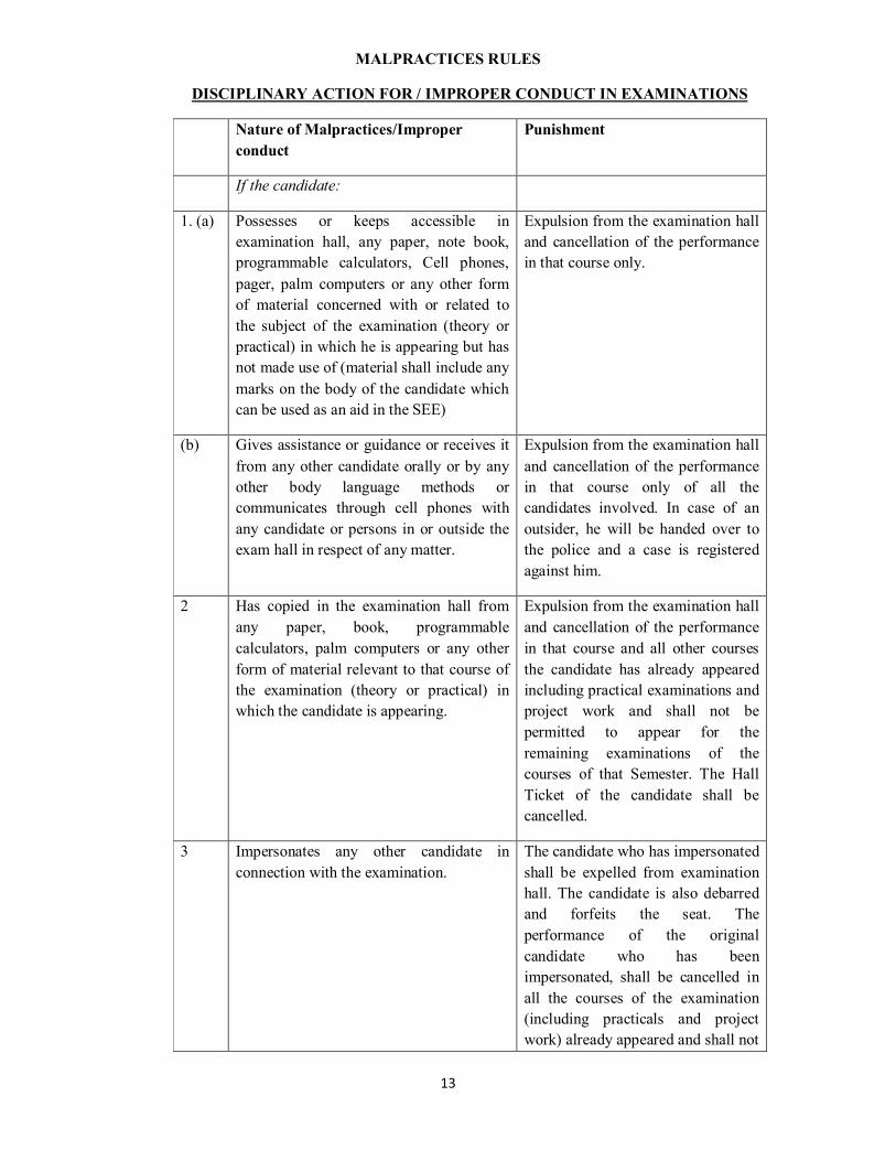
MALPRACTICES RULES
DISCIPLINARY ACTION FOR / IMPROPER CONDUCT IN EXAMINATIONS
Nature of Malpractices/Improper conduct
Punishment
If the candidate:
1. (a)
Possesses or keeps accessible in examination hall, any paper, note book, programmable calculators, Cell phones, pager, palm computers or any other form of material concerned with or related to the subject of the examination (theory or practical) in which he is appearing but has not made use of (material shall include any marks on the body of the candidate which can be used as an aid in the SEE)
Expulsion from the examination hall and cancellation of the performance in that course only.
(b)
Gives assistance or guidance or receives it from any other candidate orally or by any other body language methods or communicates through cell phones with any candidate or persons in or outside the exam hall in respect of any matter.
Expulsion from the examination hall and cancellation of the performance in that course only of all the candidates involved. In case of an outsider, he will be handed over to the police and a case is registered against him.
2
Has copied in the examination hall from any paper, book, programmable calculators, palm computers or any other form of material relevant to that course of the examination (theory or practical) in which the candidate is appearing.
Expulsion from the examination hall and cancellation of the performance in that course and all other courses the candidate has already appeared including practical examinations and project work and shall not be permitted to appear for the remaining examinations of the courses of that Semester. The Hall Ticket of the candidate shall be cancelled.
3
Impersonates any other candidate in connection with the examination.
The candidate who has impersonated shall be expelled from examination hall. The candidate is also debarred and forfeits the seat. The performance of the original candidate who has been impersonated, shall be cancelled in all the courses of the examination (including practicals and project work) already appeared and shall not
14
be allowed to appear for examinations of the remaining courses of that semester. The candidate is also debarred for two consecutive semesters from class work and all SEE. The continuation of the programme by the candidate is subject to the academic regulations in connection with forfeiture of seat. If the imposter is an outsider, he will be handed over to the police and a case is registered against him.
4
Smuggles in the Answer book or additional sheet or takes out or arranges to send out the question paper during the examination or answer book or additional sheet, during or after the examination.
Expulsion from the examination hall and cancellation of performance in that course and all the other courses the candidate has already appeared including practical examinations and project work and shall not be permitted for the remaining examinations of the courses of that semester. The candidate is also debarred for two consecutive semesters from class work and all SEE. The continuation of the programme by the candidate is subject to the academic regulations in connection with forfeiture of seat.
5
Uses objectionable, abusive or offensive language in the answer paper or in letters to the examiners or writes to the examiner requesting him to award pass marks.
Cancellation of the performance in that course.
6
Refuses to obey the orders of the Chief Controller of Examinations (CCE) / Controller of Examinations (CE) / Assistant Controller of Examinations (ACE) / any officer on duty or misbehaves or creates disturbance of any kind in and around the examination hall or organizes a walk out or instigates others to walk out, or threatens the officer-in charge or any person on duty in or outside the examination hall of any injury to his person or to any of his relations whether by words, either spoken or written or by signs or by visible representation, assaults
In case of students of the college, they shall be expelled from examination halls and cancellation of their performance in that course and all other courses the candidate(s) has (have) already appeared and shall not be permitted to appear for the remaining examinations of the courses of that semester. The candidates also are debarred and forfeit their seats. In case of outsiders, they will be handed over to the police and a
15
the officer in-charge, or any person on duty in or outside the examination hall or any of his relations, or indulges in any other act of misconduct or mischief which result in damage to or destruction of property in the examination hall or any part of the College campus or engages in any other act which in the opinion of the officer on duty amounts to use of unfair means or misconduct or has the tendency to disrupt the orderly conduct of the examination
police cases registered against them.
7
Leaves the exam hall taking away answer script or intentionally tears of the script or any part thereof inside or outside the examination hall.
Expulsion from the examination hall and cancellation of performance in that course and all the other courses the candidate has already appeared including practical examinations and project work and shall not be permitted for the remaining examinations of the courses of that semester/year. The candidate is also debarred for two consecutive semesters from class work and all SEE. The continuation of the programme by the candidate is subject to the academic regulations in connection with forfeiture of seat.
8
Possess any lethal weapon or firearm in the examination hall.
Expulsion from the examination hall and cancellation of the performance in that course and all other courses the candidate has already appeared including practical examinations and project work and shall not be permitted for the remaining examinations of the courses of that semester. The candidate is also debarred and forfeits the seat.
9
If student of the college, who is not a candidate for the particular examination or any person not connected with the college indulges in any malpractice or improper conduct mentioned in clause 6 to 8.
Expulsion from the examination hall and cancellation of the performance in that course and all other courses the candidate has already appeared including practical examinations and project work and shall not be permitted for the remaining examinations of the courses of that semester. The candidate is also
16
debarred and forfeits the seat. Person(s) who do not belong to the College will be handed over to police and, a police case will be registered against them.
10
Comes in a drunken condition to the examination hall.
Expulsion from the examination hall and cancellation of the performance in that course and all other courses the candidate has already appeared including practical examinations and project work and shall not be permitted for the remaining examinations of the courses of that semester.
11
Copying detected on the basis of internal evidence, such as, during valuation or during special scrutiny.
Cancellation of the performance in that course and all other courses the candidate has appeared including practical examinations and project work of that SEE.
12
If any malpractice is detected which is not covered in the above clauses 1 to 11 shall be reported to the CCE for further action toward suitable punishment.
Note: The student(s) found indulging in malpractices during the CIE also will be punished based on the recommendations of the College Academic Committee.
17
MALLA REDDY ENGINEERING COLLEGE (Autonomous)
Academic Year 2015-16 (Choice Based Credit System)
COURSE STRUCTURE – M.TECH VLSI System Design (VLSI SD)
(MR15 Regulations)
I SEMESTER
S. No. Category Course
Code Name of the
course
Contact hours/ week Credits
Scheme of Valuation Total
Marks L T P Internal
(CIE) External
(SEE)
1 CC I 54101 VLSI Technology and Design
4 -- -- 4 40 60 100
2 CC II 54201 CMOS Analog Integrated Circuit Design
4 -- -- 4 40 60 100
3 CC III 54107 CMOS Digital Integrated Circuit Design
4 -- -- 4 40 60 100
4 PE I
54102 Digital System Design
4 -- -- 4 40 60 100 54104
Hardware and Software Co-Design
54202 Hardware Description Language
5 PE II
54203
Algorithms for VLSI Design Automation
4 -- -- 4 40 60 100 54106
Embedded System Design
54122 Device Modeling
6 PE III
54111
Soft Computing Techniques
4 -- -- 4 40 60 100 54105
Image and Video Processing
54110 Coding Theory and Techniques
7 Laboratory I 54204 VLSI System Design Lab -- -- 4 2 40 60 100
8 Seminar I 54205 Seminar - I -- -- 4 2 100 -- 100
Total 24 -- 8 28 Contact Periods: 32
18
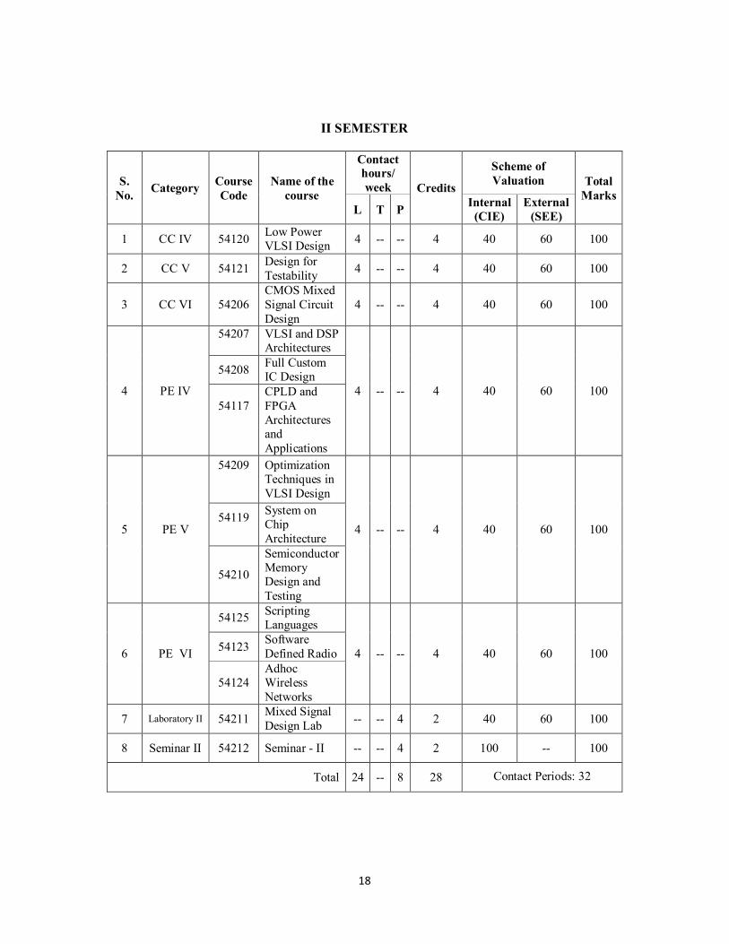
II SEMESTER
S. No. Category Course
Code Name of the
course
Contact hours/ week Credits
Scheme of Valuation Total
Marks L T P Internal
(CIE) External
(SEE)
1 CC IV 54120 Low Power VLSI Design 4 -- -- 4 40 60 100
2 CC V 54121 Design for Testability 4 -- -- 4 40 60 100
3 CC VI 54206 CMOS Mixed Signal Circuit Design
4 -- -- 4 40 60 100
4 PE IV
54207
VLSI and DSP Architectures
4 -- -- 4 40 60 100
54208 Full Custom IC Design
54117
CPLD and FPGA Architectures and Applications
5 PE V
54209
Optimization Techniques in VLSI Design
4 -- -- 4 40 60 100 54119
System on Chip Architecture
54210
Semiconductor Memory Design and Testing
6 PE VI
54125 Scripting Languages
4 -- -- 4 40 60 100 54123 Software Defined Radio
54124 Adhoc Wireless Networks
7 Laboratory II 54211 Mixed Signal Design Lab -- -- 4 2 40 60 100
8 Seminar II 54212 Seminar - II -- -- 4 2 100 -- 100
Total 24 -- 8 28 Contact Periods: 32
19
III Semester
S. No. Category Course
Code Name of the
course
Contact hours/ week Credits
Scheme of Valuation
Total Marks
L T P Internal
(CIE) External
(SEE)
1 CV 54213 Comprehensive
Viva-Voce -- -- -- 4 -- 100 100
2 PR I 54214 Project work
Part I -- -- 16 8 50 -- 50
Total -- -- 16 12 Contact Periods: 16
IV Semester
S. No. Category Course
Code Name of
the course
Contact hours/week
Credits
Scheme of Valuation Total
Marks L T P Internal
(CIE) External
(SEE)
1 PR II 54215 Project
work Part II -- -- 16 8 50 -- 50
2 PR III 54216 Project
Viva-Voce -- -- -- 12 -- 150 150
Total -- -- 16 20 Contact Periods: 16
* CC – Core Course, PE – Professional Elective, CV – Comprehensive Viva – Voce, PR – Project Work
20
2015-16
Malla Reddy Engineering College (Autonomous) L T P
4 - - Course Code: 54101 Credits: 4
M.Tech. – I Semester VLSI TECHNOLOGY AND DESIGN
PREREQUISITES: STLD and IC Technology
OBJECTIVE: To Understand the VLSI technology and design of circuits based on technology like cmos, bicmos etc, to understand the designing layouts of logic gates, to understanding the combinational logic networks and its optimization, to understanding the sequential systems and its optimization, to get knowledge on floor plan design
Module –I [10 Periods]
Crystal Growth and Wafer Preparation: Introduction, Electronic-Grade Silicon, Czochralski Crystal Growing, Silicon Shaping, Process Considerations.
Oxidation: Thin Oxides, Oxidation Techniques and Systems, Oxide properties, Redistribution of Dopant At interface, Oxidation of Poly Silicon, Oxidation inducted Defects
Module –II [9 Periods]
Lithography: Introduction, Optical Lithography, Electron Lithography, X-ray Lithography, Ion Lithography.
Reactive Plasma Etching: Introduction, Plasma Properties, Feature-Size Control and Anisotropic Etch Mechanisms, Other Properties of Etch Processes, Reactive Plasma-Etching Techniques and Equipment, Specific Etch Processes.
Module –III [8 Periods]
Dielectric and Polysilicon Film Deposition: Introduction, Deposition Processes, Polysilicon, Silicon Dioxide, Silicon Nitride, Plasma Assisted Depositions, Other Materials. Diffusion: Models of Diffusion in Solids, Flick’s one Dimensional Diffusion Equation – Atomic Diffusion Mechanism – Measurement techniques Module -IV [9 Periods] Ion Implantation: Introduction, Range Theory, Implantation Equipment, Annealing, Shallow Junctions, High-Energy Implantation. Metallization: Introduction, Metallization Applications, Metallization Choices, Physical Vapor Deposition, Patterning, Metallization Problems..
Basic Electrical Properties of MOS and BICMOS circuits :Ids-Vds relationships, MOS transistor threshold Voltage(Vt), Pass transistor, NMOS Inverter, Determination of pull-up to pull-down ratios, Various pull ups of MOS and BICMOS inverter, Lambda based Design Rules
Text Books: 1. S. M. Sze, “VLSI Technology”, McGraw-Hill, Second Edition,2003,TMH NewDelhi. 2. Kamran Eshraghian, Eshraghian Dougles and A. Pucknell, Essentials of VLSI circuits and systems –2005, PHI New Delhi. Reference Books: 1. S.K. Ghandhi, "VLSI Fabrication Principles", John Wiley Inc., Second Edition New York, 1994.
COURSE OUTCOMES:
After completion of the course, students will be able to:
1.Student will be in a position that he/she can design vlsi circuits starting from pmos nmos, cmos, and bicmos technology based design
2.Gains thorough knowledge on design tools to draw layouts for the transistor structures 3.The student will understand the design of logic gates 4.The student will understand the design of sequential systems
22
2015-16 Malla Reddy Engineering College (Autonomous)
L T P 4 - -
Course Code: 54201 Credits: 4 M.Tech. – I Semester
CMOS ANALOG INTEGRATED CIRCUIT DESIGN PREREQUISITES: CMOS and VLSI Technology. OBJECTIVE: To learn about MOS Transistor, Passive Components- Capacitor & Resistor, Integrated circuit Layout, CMOS Device Modeling - Simple MOS Large-Signal Model, Small-Signal Model for the MOS Transistor, to learn about Design of CMOS Op Amps, Compensation of Op Amps, Design of Two-Stage Op Amps, Power Supply Rejection Ratio of Two-Stage Op Amps, Cascade Op Amps, Measurement Techniques of OP Amp, to know about Characterization of Comparator, Two-Stage, Open-Loop Comparators, Other Open-Loop Comparators, Improving the Performance of Open-Loop Comparators, Discrete-Time Comparators
Module - I: MOS DEVICES AND MODELING [9 Periods] The MOS Transistor, Passive Components- Capacitor & Resistor, Integrated circuit Layout, CMOS Device Modeling - Simple MOS Large-Signal Model, Other Model Parameters, Small-Signal Model forth MOS Transistor, Computer Simulation Models, Sub-threshold MOS Model. Module -II: ANALOG CMOS SUB-CIRCUITS [9 Periods] MOS Switch, MOS Diode, MOS Active Resistor, Current Sinks and Sources, Current Mirrors-Current mirror with Beta Helper, Degeneration, Cascade current Mirror and Wilson Current Mirror, Current and Voltage References, Band gap Reference. Module -III: CMOS AMPLIFIERS [8 Periods] Inverters, Differential Amplifiers, Cascade Amplifiers, Current Amplifiers, Output Amplifiers, High Gain Amplifiers Architectures. Module -IV: CMOS OPERATIONAL AMPLIFIERS [9 Periods] Design of CMOS Op Amps, Compensation of Op Amps, Design of Two-Stage Op Amps, Power Supply Rejection Ratio of Two-Stage Op Amps, Cascade Op Amps, Measurement Techniques of OP Amp. Module -V: COMPARATORS [9 Periods] Characterization of Comparator, Two-Stage, Open-Loop Comparators, other Open-Loop Comparators, Improving the Performance of Open-Loop Comparators, Discrete-Time Comparators. TEXT BOOKS: 1. Philip E. Allen and Douglas R. Holberg,CMOS Analog Circuit Design,Oxford UniversityPress, International Second Edition/Indian Edition, 2010. 2. Paul R. Gray, Paul J. Hurst, S. Lewis andR. G. Meyer,Analysis and Design of Analog Integrated Circuits,Wiley India, Fifth Edition, 2010.
23
REFERENCE BOOKS: 1. David A. Johns, Ken Martin, Analog Integrated Circuit Design, Wiley Student Edn, 2013. 2. Behzad Razavi, Design of Analog CMOS Integrated Circuits, TMH Edition. 3. Baker, Li and Boyce, CMOS: Circuit Design, Layout and Simulation, PHI.
COURSE OUTCOMES: After completion of the course, students will be able to:
1. Learn about MOS Transistor, Passive Components- Capacitor & Resistor, Integrated circuit Layout, CMOS Device Modeling - Simple MOS Large-Signal Model, Small-Signal Model for the MOS Transistor.
2. Learn about Design of CMOS Op Amps, Compensation of Op Amps, Design of Two-Stage Op Amps, and Power Supply Rejection Ratio of Two-Stage Op Amps, Cascade Op Amps, and Measurement Techniques of OP Amp.
3. Know about Characterization of Comparator, Two-Stage, Open-Loop Comparators, Other Open-Loop Comparators, Improving the Performance of Open-Loop Comparators, Discrete-Time Comparators
24
2015-16 Malla Reddy Engineering College (Autonomous)
L T P 4 - -
Course Code: 54107 Credits: 4 M.Tech. – I Semester
CMOS DIGITAL INTEGRATED CIRCUIT DESIGN
PREREQUISITES: VLSI Technology and IC Design OBJECTIVE: To teach fundamentals of CMOS Digital integrated circuit design such as importance of Pseudo logic, Combinational MOS logic circuits, Sequential MOS logic circuits, To teach the fundamentals of Dynamic logic circuits and basic semiconductor memories which are the basics for the design of high performance digital integrated circuits. Module - I [10 Periods] MOS DESIGN: Pseudo NMOS Logic – Inverter, Inverter threshold voltage, Output high voltage, Output Low voltage, Gain at gate threshold voltage, Transient response, Rise time, Fall time, Pseudo NMOS logic gates, Transistor equivalency, CMOS Inverter logic. Module - II [8 Periods] COMBINATIONAL MOS LOGIC CIRCUITS:MOS logic circuits with NMOS loads, Primitive CMOS logic gates – NOR & NAND gate, Complex Logic circuits design – Realizing Boolean expressions using NMOS gates and CMOS gates , AOI and OIA gates, CMOS full adder, CMOS transmission gates, Designing with Transmission gates. Module - III [7 Periods] SEQUENTIAL MOS LOGIC CIRCUITS: Behavior of bistable elements, SR Latch, Clocked latch and flip flop circuits, CMOS D latch and edge triggered flipflop. Module - IV [10 Periods] DYNAMIC LOGIC CIRCUITS: Basic principle, Voltage Bootstrapping, Synchronous dynamic pass transistor circuits, Dynamic CMOS transmission gate logic, High performance Dynamic CMOS circuits. Module - V [8 Periods] SEMICONDUCTOR MEMORIES: Types, RAM array organization, DRAM – Types, Operation, Leakage currents in DRAM cell and refresh operation, SRAM operation Leakage currents in SRAM cells, Flash Memory- NOR flash and NAND flash. TEXT BOOKS 1. Ken Martin, Digital Integrated Circuit Design, Oxford University Press, 2011. 2. Sung-Mo Kang, Yusuf Leblebici, CMOS Digital Integrated Circuits Analysis and Design, TMH, 3rd Ed., 2011. REFERENCE BOOKS 1. Ming-BO Lin, Introduction to VLSI Systems: A Logic, Circuit and System Perspective, CRC Press, 2011 2. Jan M. Rabaey, AnanthaChandrakasan, BorivojeNikolic ,Digital Integrated Circuits – A Design Perspective , 2nd Ed,PHI.
25
COURSE OUTCOMES: After completion of the course, students will be able to:
1. Able to understand the realization of different logic circuit designs for logic expressions and the importance of the circuit designs , the drawback of the designs both in combinational as well as sequential.
2. Able to know different types of memories , performance evaluation of each memory modules they can be able to think how to improve performance by taking different structures
26
2015-16 Malla Reddy Engineering College (Autonomous)
L T P 4 - -
Course Code: 54102 Credits: 4 M.Tech. – I Semester
DIGITAL SYSTEM DESIGN (Professional Elective - I)
PREREQUISITES: VLSI and STLD OBJECTIVE: To impart knowledge on the theory of Sequential machines and minimization of it. to design digital circuits for various applications. to learn fault diagnosis and testability algorithms.
MODULE – I :Minimization And Transformation Of Sequential Machines [8 Periods]
The Finite State Model – Capabilities and limitations of FSM – State equivalence and machine minimization – Simplification of incompletely specified machines. Fundamental mode model – Flow table – State reduction – Minimal closed covers – Races, Cycles and Hazards.
MODULE – II : Digital Design [9 Periods]
Digital Design Using ROMs, PALs and PLAs, BCD Adder, 32 – bit adder, State graphs for control circuits, Scoreboard and Controller, A shift and add multiplier, Array multiplier, Keypad Scanner, Binary divider.
MODULE – III: SM Charts [7 Periods]
State machine charts, Derivation of SM Charts, Realization of SM Chart, Implementation of Binary Multiplier, dice game controller.
Logic Fault model – Fault detection & Redundancy- Fault equivalence and fault location –Fault dominance – Single stuck at fault model – Multiple stuck at fault models –Bridging fault model. Fault diagnosis of combinational circuits by conventional methods – Path sensitization techniques, Boolean Difference method – Kohavi algorithm – Test algorithms – D algorithm, PODEM, Random testing, Transition count testing, Signature analysis and test bridging faults.
MODULE – V: Fault Diagnosis in Sequential Circuits [7 Periods]
Circuit Test Approach, Transition Check Approach – State identification and fault detection experiment, Machine identification, Design of fault detection experiment TEXT BOOKS:
1. Charles H. Roth, Fundamentals of Logic Design ,Cengage Learning,5th Ed.
2. MironAbramovici, Melvin A. Breuer and Arthur D. Friedman , Digital Systems
Testing and Testable Design, John Wiley & Sons Inc.
27
3. N. N. Biswas ,Logic Design Theory , PHI.
REFERENCE BOOKS:
1. Z. Kohavi ,Switching and Finite Automata Theory, TMH, 2nd Ed,2001.
COURSE OUTCOMES: After completion of the course, students will be able to:
1. Design digital circuits by their own for new applications. 2. Identify techniques to improve fault diagnosis for digital circuits.
28
2015-16 Malla Reddy Engineering College (Autonomous)
L T P 4 - -
Course Code: 54104 Credits: 4 M.Tech. – I Semester
HARDWARE AND SOFTWARE CO-DESIGN (Professional Elective - I)
PREREQUISITES: Models and Architectures OBJECTIVE: To design mixed hardware-software systems and the design of hardware-software interfaces, To focus on common underlying modeling concepts, and the trade-offs between hardware and software components, To learn about System –level specification, design representation for system level synthesis, system level specification languages. Module –I: Co- Design Issues [10 Periods] Co- Design Models, Architectures, Languages, A Generic Co-design Methodology. Co- synthesis algorithms: Hardware software synthesis algorithms: hardware – software partitioning distributed system co synthesis. Module –II: Prototyping and Emulation [8 Periods] Prototyping and emulation techniques, prototyping and emulation environments, future developments in emulation and prototyping architecture specialization techniques, system communication infrastructure Target architectures: Architecture Specialization techniques, System Communication infrastructure, Target Architecture and Application System classes, Architecture for control dominated systems (8051-Architectures for High performance control), Architecture for Data dominated systems (ADSP21060, TMS320C60), Mixed Systems. Module –III: Compilation Techniques and Tools for Embedded Processor Architectures [8 Periods] Modern embedded architectures, embedded software development needs, compilation technologies, practical consideration in a compiler development environment. Module –IV: Design Specification and Verification [10 Periods] Design, co-design, the co-design computational model, concurrency coordinating concurrent computations, interfacing components, design verification, implementation verification, verification tools, interface verification Module –V: Languages For System – Level Specification And Design-I [9 Periods] System – level specification, design representation for system level synthesis, system level specification languages, Languages for system – level specification and design-ii: Heterogeneous specifications and multi language co-simulation, the cosyma system and lycossystem. TEXT BOOKS: 1. Jorgen Staunstrup, Wayne Wolf, Hardware / Software Co- Design Principles and Practice, Springer, 2009. 2. Giovanni De Micheli, Mariagiovanna Sami, Hardware / Software Co- Design ,KluwerAcademic Publishers,2002.
29
REFERENCE BOOKS: 1. Patrick R. Schaumont , A Practical Introduction to Hardware/Software Co-design, Springer,2010. COURSE OUTCOMES: After completion of the course, students will be able to:
1. Able to design mixed hardware-software systems and the design of hardware-software interfaces
2. Able to focus on common underlying modeling concepts, , and the trade-offs between hardware and software components.
3. Able to learn about System –level specification, design representation for system level synthesis, system level specification languages.
30
2015-16 Malla Reddy Engineering College (Autonomous)
L T P 4 - -
Course Code: 54202 Credits: 4 M.Tech – I Semester
HARDWARE DESCRIPTION LANGUAGE (Professional Elective - I)
PREREQUISITES: Digital Circuits. OBJECTIVE: This course provides the knowledge to design Digital Circuits behavioral and RTL modeling using Verilog HDL. And also verifying these models and synthesizing RTL models to standard cell libraries and FPGAs. This course also provides different technologies related to HDLs, construct, compile and execute Verilog HDL programs using provided software tools. MODULE - I: Introduction to Verilog HDL [12 Periods] Verilog as HDL, Levels of Design Description, Concurrency, Simulation and Synthesis, Function Verification, System Tasks, Programming Language Interface, Module, Simulation and Synthesis Tools. Language Constructs and Conventions: Introduction, Keywords, Identifiers, White space Characters, Comments, Numbers, Strings, Logic Values, Strengths, Data types, Scalars and Vectors, Parameters, Operators. MODULE - II: Gate Level & Data Flow Modeling [12 Periods] Gate Level Modeling: Introduction, AND Gate Primitive, Module Structure, Other Gate Primitives, Illustrative Examples, Tristate Gates, Array of Instances of Primitives, Design of Flip –Flops with Gate Primitives, Delays, Strengths and Construction Resolution, Net Types, Design of Basic Circuit. Modeling at Dataflow Level: Introduction to Continuous Assignment Structure, Delays and Continuous Assignments, Assignment to Vectors, Operators. MODULE - III: Behavioral Modeling [12 Periods] Introduction, Operations and Assignments, Functional Bifurcation, ‘Initial’ Construct, ‘Always’ Construct, Assignments with Delays, ‘Wait’ Construct, Multiple Always Block, Designs at Behavioral Level, Blocking and Non- Blocking Assignments, The ‘Case’ Statement, Simulation Flow ‘If’ an ‘If-Else’ Constructs, ‘Assign- De-Assign’ Construct, ‘Repeat’ Construct, for Loop, ‘The Disable’ Construct, ‘While Loop’, Forever Loop, Parallel Blocks, ‘Force- Release, Construct, Event. MODULE - IV: Switch Level Modeling [12 Periods] Switch Level Modeling: Basic Transistor Switches, CMOS Switches, Bi Directional Gates, Time Delays With Switch Primitives, Instantiation with ‘Strengths’ and ‘Delays’, Strength Contention with Trireg Nets. System Tasks, Functions and Compiler Directives: Parameters, Path Delays, Module Parameters, System Tasks and Functions, File Based Tasks and Functions, Computer Directives, Hierarchical Access, User Defined Primitives. MODULE - V: Sequential Circuit Description and Testing [12 Periods] Sequential Circuit Description: Sequential Models - Feedback Model, Capacitive Model, Implicit Model, Basic Memory Components, Functional Register, Static Machine Coding, Sequential Synthesis.
31
Component Test and Verification: Test Bench- Combinational Circuit Testing, Sequential Circuit Testing, Test Bench Techniques, Design Verification, Assertion Verification. TEXT BOOKS:
1. T R. Padmanabhan, B Bala Tripura Sundari, “Design Through Verilog HDL”, Wiley, 2009. (Modules I, II, III, IV & V)
2. Zainalabdien Navabi, “Verilog Digital System Design”, TMH, 2nd Edition, 1999. (Modules I, II, III, IV & V)
REFERENCE BOOKS:
1. Stephen Brown, Zvonkoc Vranesic, “Fundamentls of Digital Logic with Veilog Design”, TMH, 2nd Edition, 2010.
2. Sunggu Lee, “Advanced Digital Logic Design using Verilog, State Machine & Synthesis for FPGA”, Cengage Learning, 2012.
3. Samir Palnitkar, “Verilog HDL”, Pearson Education, 2nd Edition, 2009. 4. Michel D. Ciletti, “Advanced Digital Design with the Verilog HDL”, PHI, 2009.
COURSE OUTCOMES:
After completion of the course, students will be able to: 1. Understand Verilog hardware description languages (HDL) to design Digital Circuits
in different Models. 2. Write Register Transfer Level (RTL) models of digital circuits. 3. Describe standard cell libraries and FPGAs. 4. Synthesize RTL models to standard cell libraries and FPGAs. 5. Test the Digital Circuits using Test bencehes.
32
2015-16 Malla Reddy Engineering College (Autonomous)
L T P 4 - -
Course Code: 54203 Credits: 4 M.Tech. – I Semester
ALGORITHMS FOR VLSI DESIGN AUTOMATION (Professional Elective –II) PREREQUISITE: VLSI and Designing Techniques. OBJECTIVES: To Introduce the VLSI Algorithms and Automation Techniques Module - I : PRELIMINARIES [09 Periods] Introduction to Design Methodologies, Design Automation tools, Algorithmic Graph Theory, Computational complexity, Tractable and Intractable problems. Module – II: GENERAL PURPOSE METHODS FOR COMBINATIONAL OPTIMIZATION [09 Periods] Backtracking, Branch and Bound, Dynamic Programming, Integer Linear Programming, Local Search, Simulated Annealing, Tabu search, Genetic Algorithms. Module – III: [09 Periods] LAYOUT COMPACTION, PLACEMENT, FLOORPLANNING AND ROUTING Problems, Concepts and Algorithms. MODELLING AND SIMULATION Gate Level Modelling and Simulation, Switch level Modelling and Simulation. Module – IV: [09 Periods] LOGIC SYNTHESIS AND VERIFICATION Basic issues and Terminology, Binary-Decision diagrams, Two-Level logic Synthesis HIGH-LEVEL SYNTHESIS Hardware Models, Internal representation of the input Algorithm, Allocation, Assignment and Scheduling, Some Scheduling Algorithms, Some aspects of Assignment problem, High-level Transformations. Module – V: [09 Periods] PHYSICAL DESIGN AUTOMATION OF FPGAs FPGA technologies, Physical Design cycle for FPGAs, partitioning and Routing for segmented and staggered Models. PHYSICAL DESIGN AUTOMATION OF MCMs MCM technologies, MCM physical design cycle, Partitioning, Placement - Chip Array based and Full Custom Approaches, Routing – Maze routing, Multiple stage routing, Topologic routing, Integrated Pin – Distribution and routing, Routing and Programmable MCMs. TEXT BOOKS 1. S.H.Gerez, Algorithms for VLSI Design Automation, WILEY Student Edition, 1999,
John wiley& Sons (Asia) Pvt. Ltd. 2. NaveedSherwani, Algorithms for VLSI Physical Design Automation, Springer
International Edition, 3rd Ed., 2005,.
33
REFERENCE BOOKS 1. Hill & Peterson, Computer Aided Logical Design with Emphasis on
VLSI,Wiley,1993, 2. Wayne Wolf, Modern VLSI Design:Systems on silicon, Pearson Education Asia,2nd ed.,
1998.
COURSE OUTCOMES: At the end of the course students are able to:
1. Knowledge on VLSI Algorithms 2. General Methods Algorithms Synthesis Algorithms
34
2015-16 Malla Reddy Engineering College (Autonomous)
L T P 4 - -
Course Code: 54106 Credits: 4 M.Tech. – I Semester
EMBEDDED SYSTEM DESIGN (Professional Elective – II)
PREREQUISITES: Microprocessors and Microcontrollers. OBJECTIVE: This course introduces the difference between Embedded Systems and General purpose systems. This course familiarizes to compare different approaches in optimizing General purpose processors. This course provides the design tradeoffs made by different models of embedded systems. Module - I: Introduction to Embedded Systems [08 Periods] Definition of Embedded System, Embedded Systems Vs General Computing Systems, History of Embedded Systems, Classification, Major Application Areas, Purpose of Embedded Systems, Characteristics and Quality Attributes of Embedded Systems. Module - II: Typical Embedded System [12 Periods] Core of the Embedded System: General Purpose and Domain Specific Processors, ASICs, PLDs, Commercial Off-The-Shelf Components (COTS), Memory: ROM, RAM, Memory according to the type of Interface, Memory Shadowing, Memory selection for Embedded Systems, Sensors and Actuators, Communication Interface: Onboard and External Communication Interfaces. Module - III: Embedded Firmware [10 Periods] Reset Circuit, Brown-out Protection Circuit, Oscillator Unit, Real Time Clock, Watchdog Timer, Embedded Firmware Design Approaches and Development Languages. Module - IV: RTOS Based Embedded System Design [12 Periods] Operating System Basics, Types of Operating Systems, Tasks, Process and Threads, Multiprocessing and Multitasking, Task Scheduling. Module - V: Task Communication [08 Periods] Shared Memory, Message Passing, Remote Procedure Call and Sockets, Task Synchronization: Task Communication/Synchronization Issues, Task Synchronization Techniques, Device Drivers, How to Choose an RTOS. TEXT BOOKS:
1. Shibu K. V, “Introduction to Embedded Systems”, McGraw Hill, 2013. (Modules I, II, III, IV & V)
REFERENCE BOOKS: 1. Raj Kamal, “Embedded Systems”, TMH. 2. Frank Vahid, Tony Givargis, John Wiley, “Embedded System Design”. 3. Lyla , “Embedded Systems”, Pearson, 2013. 4. David E. Simon, “An Embedded Software Primer”, Pearson Education.
35
COURSE OUTCOMES: At the end of the course students are able to:
1. Understand the basics of an embedded system. 2. Design, implement and test an embedded system. 3. Understand the design tradeoffs made by different models of embedded systems.
36
2015-16 Malla Reddy Engineering College (Autonomous)
L T P 4 - -
Course Code: 54122 Credits: 4 M.Tech. – I Semester
DEVICE MODELLING (Professional Elective – II)
PREREQUISITES: Engineering Physics and Semiconductor Physics OBJECTIVE: To know about Quantum Mechanics, Boltzman transport equation, Continuity equation, Poisson equation , To learn about Types and structures in monolithic technologies – Basic model (Eber-Moll) – Gunmel - Poon model dynamic model, Parasitic effects – SPICE model –Parameter extraction , To learn about An overview of wafer fabrication, Wafer Processing – Oxidation –Patterning – Diffusion – Ion Implantation – Deposition – Silicon gate nMOS process – CMOS Module - I: [8 Periods] INTRODUCTION TO SEMICONDUCTOR PHYSICS: Review of Quantum Mechanics, Boltzman transport equation, Continuity equation, Poisson equation. Integrated Passive Devices: Types and Structures of resistors and capacitors in monolithic technology, Dependence of model parameters on structures Module -II: [9 Periods] INTEGRATED DIODES: Junction and Schottky diodes in monolithic technologies – Static and Dynamic behavior – Small and large signal models – SPICE models Integrated Bipolar Transistor: Types and structures in monolithic technologies – Basic model (Eber-Moll) – Gunmel - Poon model dynamic model, Parasitic effects – SPICE model –Parameter extraction. Module - III: [11 Periods] INTEGRATED MOS TRANSISTOR:NMOS and PMOS transistor – Threshold voltage – Threshold voltage equations – MOS device equations – Basic DC equations second order effects – MOS models – small signal AC characteristics– MOS FET SPICE model level 1, 2, 3 and 4. Module - IV: [10 Periods] VLSI FABRICATION TECHNIQUES: An overview of wafer fabrication, Wafer Processing – Oxidation –Patterning – Diffusion – Ion Implantation – Deposition – Silicon gate nMOS process – CMOS processes – n-well- p-well- twin tub- Silicon on insulator – CMOS process enhancements –Interconnects circuit elements Module - V: [8 Periods] MODELING OF HETERO JUNCTION DEVICES: Band gap Engineering, Band gap Offset at abrupt Hetero Junction, Modified current continuity equations, Hetero Junction bipolar transistors (HBTs), SiGe TEXT BOOKS: 1. Tyagi M. S, Introduction to Semiconductor Materials and Devices, John Wiley Student Edition,2008. 2. Ben G. Streetman, Solid State Circuits, Prentice Hall, 1997
37
REFERENCE BOOKS: 1. Sze S. M, Physics of Semiconductor Devices, Mcgraw Hill ,2nd Edition, New York, 1981. 2. Tor A. Fijedly, Introduction to Device Modeling and Circuit Simulation ,Wiley- Interscience, 1997. 3. Ming-BO Lin, Introduction to VLSI Systems: A Logic, Circuit and System Perspective , CRC Press, 2011
COURSE OUTCOMES: At the end of the course students are able to:
1. Know about Quantum Mechanics, Boltzman transport equation, Continuity equation, Poisson equation.
2. Learn about Types and structures in monolithic technologies – Basic model (Eber-Moll) – Gunmel - Poon model dynamicmodel, Parasitic effects – SPICE model –Parameter extraction.
3. Learn about An overview of wafer fabrication, Wafer Processing – Oxidation –Patterning – Diffusion – Ion Implantation – Deposition – Silicon gate nMOS process – CMOS
38
2015-16 Malla Reddy Engineering College (Autonomous)
L T P 4 - -
Course Code: 54111 Credits: 4 M.Tech. – I Semester
PREREQUISITES: Neural Networks and Fuzzy Logic Systems. OBJECTIVE: To know about Approaches to intelligent control, Architecture for intelligent control, Symbolic reasoning system, Rule based systems, To know about Concept of Artificial Neural Networks and its basic mathematical model, McCulloch-Pitts neuron model, simple perception, Adeline and Madeline, Feed-forward Multilayer Perceptron, Learning and Training the neural network, To learn about fuzzy sets, basic fuzzy set operation and approximate reasoning, Introduction to fuzzy logic modeling and control, Fuzzification, inferencing and defuzzification, Fuzzy knowledge and rule bases, Fuzzy modeling Module – I: Introduction [10 Periods] Approaches to intelligent control, Architecture for intelligent control, Symbolic reasoning system, Rule based systems, the AI approach, Knowledge representation - Expert systems. Module - II: Artificial Neural Networks [9 Periods] Concept of Artificial Neural Networks and its basic mathematical model, McCulloch-Pitts neuron model, simple perceptron, Adaline and Madaline, Feed-forward Multilayer Perceptron, Learning and Training the neural network, Data Processing: Scaling, Fourier transformation, principal-component analysis and wavelet transformations, Hopfield network, Self-organizing network and Recurrent network, Neural Network based controller. Module - III: Fuzzy Logic System [8 Periods] Introduction to crisp sets and fuzzy sets, basic fuzzy set operation and approximate reasoning,Introduction to fuzzy logic modeling and control, Fuzzification, inferencing and defuzzification, Fuzzy knowledge and rule bases, Fuzzy modeling and control schemes for nonlinear systems, Selforganizing fuzzy logic control, Fuzzy logic control for nonlinear time delay system. Module - IV: Genetic Algorithm [10 Periods] Basic concept of Genetic algorithm and detail algorithmic steps, Adjustment of free parameters, Solution of typical control problems using genetic algorithm, Concept on some other search techniques like Tabu search and D-colony search techniques for solving optimization problems. Module - V: Applications [11 Periods] GA application to power system optimization problem, Case studies: Identification and control of linear and nonlinear dynamic systems using MATLAB-Neural Network toolbox, Stability analysis of Neural-Network interconnection systems, Implementation of fuzzy logic controller using MATLAB fuzzy-logic toolbox, Stability analysis of fuzzy control systems.
39
TEXT BOOKS: 1. Jacek.M.Zurada , Introduction to Artificial Neural Systems, Jaico Publishing House, 1999. 2. Kosko, B., Prentice, Neural Networks and Fuzzy Systems, Hall of India Pvt. Ltd., 1994. REFERENCE BOOKS:
1. Klir G.J. & Folger T.A, Fuzzy Sets, Uncertainty and Information, Prentice-Hall of India Pvt.Ltd, 1993.
2. Zimmerman H.J, Fuzzy Set Theory and Its Applications, Kluwer Academic Publishers, 1994.
COURSE OUTCOMES:
After completion of the course, students will be able to:
1. Know about Approaches to intelligent control, Architecture for intelligent control, Symbolic reasoning system, Rule based systems.
2. Know about Concept of Artificial Neural Networks and its basic mathematical model, McCulloch-Pitts neuron model, simple perception, Adeline and Madeline, Feed-forward Multilayer Perceptron, Learning and Training the neural network.
3. Learn about fuzzy sets, basic fuzzy set operation and approximate reasoning, Introduction to fuzzy logic modeling and control, Fuzzification, inferencing and defuzzification, Fuzzy knowledge and rule bases, Fuzzy modeling
40
2015-16 Malla Reddy Engineering College (Autonomous)
L T P 4 - -
Course Code: 54105 Credits: 4 M.Tech. – I Semester
IMAGE AND VIDEO PROCESSING (Professional Elective - III)
PREREQUISITES: Image and Video Transformations. OBJECTIVE: To learn about Digital image fundamentals, image transforms, image enhancement, image segmentation and image compression techniques. to learn basics of video representation and video compression techniques and standards. Module - I: Fundamentals of Image Processing and Image Transforms [9 Periods] Basic steps of Image Processing System Sampling and Quantization of an image, Basic relationship between pixels. Image Segmentation: Segmentation concepts, Point, Line and Edge Detection, Thresholding, Region based segmentation. Module - II: Image Enhancement [8 Periods] Spatial domain methods: Histogram processing, Fundamentals of Spatial filtering, Smoothing spatial filters, Sharpening spatial filters. Frequency domain methods: Basics of filtering in frequency domain, image smoothing, imagesharpening, Selective filtering. Module – III: Image Compression [8 Periods] Image compression fundamentals - Coding Redundancy, Spatial and Temporal redundancy, Compression models: Lossy& Lossless, Huffman coding, Bit plane coding, Transform coding,Predictive coding, Wavelet coding, Lossy Predictive coding, JPEG Standards. Module - IV: Basic Steps of Video Processing [10 Periods] Analog Video, Digital Video. Time-Varying Image Formation models: Three-Dimensional Motion Models, Geometric Image Formation, Photometric Image Formation, Sampling of Video signals, filtering operations. Module - V: 2-D Motion Estimation [8 Periods] Optical flow, General Methodologies, Pixel Based Motion Estimation, Block- Matching Algorithm, Mesh based Motion Estimation, Global Motion Estimation, Region based Motion Estimation, Multi resolution motion estimation, Waveform based coding, Block based transform coding, Predictive coding, Application of motion estimation in Video coding. TEXT BOOKS: 1. Gonzaleze and Woods, Digital Image Processing , Pearson ,3rd Ed. 2. Yao Wang, JoemOstermann and Ya–quin Zhang,Video Processing and Communication , PH Int, 1st Ed.,. REFRENCE BOOKS: 1. ScotteUmbaugh, Digital Image Processing and Analysis-Human and Computer Vision Application with CVIP Tools, CRC Press, 2nd Ed, 2011. 2. M. Tekalp , Digital Video Processing , Prentice Hall International.
41
3. S.Jayaraman, S.Esakkirajan, T.Veera Kumar , Digital Image Processing ,TMH, 2009. 4. John Woods,Multidimentional Signal, Image and Video Processing and Coding, Ed,Elsevier, 2nd. 5. Vipula Singh , Digital Image Processing with MATLAB and Lab view, Elsevier. 6. Keith Jack ,Video Demystified – A Hand Book for the Digital Engineer, Elsevier, 5th Ed.
COURSE OUTCOMES: After completion of the course, students will be able to:
1. Understand Digital imaging fundamentals, will get working level knowledge on DCT, DFT, FFT on images, various image enhancement & segmentation techniques
2. Understand the basic of video production, representation, pixel decimation, pixel interpolation, video compression techniques in MPEG-1/2/4/H.264.
42
2015-16 Malla Reddy Engineering College (Autonomous)
L T P 4 - -
Course Code: 54110 Credits: 4 M.Tech. – I Semester
CODING THEORY AND TECHNIQUES (Professional Elective –III)
PREREQUISITES: Coding Techniques OBJECTIVE: To know about the Information theory and source coding techniques. to learn concepts of channel coding techniques. Module - I: Source Coding [10 Periods] Mathematical model of Information, A Logarithmic Measure of Information, Average and Mutual Information and Entropy, coding for discrete less sources, Source coding theorem, fixed length and variable length coding, properties of prefix codes, Shannon- Fano coding, Huffman code, Huffman code applied for pair of symbols, efficiency calculations, Lempel-Ziv codes. Module - II: Linear Block Codes [8 Periods] Introduction to Linear block codes, Generator Matrix, Systematic Linear Block codes, Encoder Implementation of Linear Block Codes, Parity Check Matrix, Syndrome testing, Error Detecting and correcting capability of Linear Block codes. Hamming Codes, Probability of an undetected error for linear codes over a Binary Symmetric Channel, Weight Enumerators and Mac-Williams identities, Perfect codes, Application of Block codes for error control in data storage Systems. Module - III: Cyclic Codes [9 Periods] Algebraic structure of cyclic codes, Binary Cyclic code properties, Encoding in systematic and non-systematic form, Encoder using (n-k) bit shift register, Syndrome Computation and Error detection, Decoding of Cyclic Codes. Module - IV: Convolution Codes [10 Periods] Encoding of Convolution codes, Structural properties of Convolutional codes, state diagram, Tree diagram, Trellis Diagram, maximum, Likelihood decoding of Convolutional codes.Viterbi Algorithm, Fano, Stack Sequential decoding algorithms, Application of Viterbi and sequential decoding. Module - V: BCH Codes [11 Periods] Groups, fields, binary Fields arithmetic, construction of Falois fields GF (2m), Basic properties of Falois Fields, Computation using Falois Field GF (2m) arithmetic, Description of BCH codes, Decoding procedure for BCH codes. TEXT BOOKS:
1. SHU LIN and Daniel J. Costello, Error Control Coding – Fundamentals and Applications, Jr. Prentice Hall Inc.
2. Fundamental and Application by Bernard Sklar , Digital Communications , Pearson Education Asia.
3. Man Young Rhee, Error Control Coding Theory, Mc. Graw Hill Publ.
43
REFERENCE BOOKS: 1. John G. Proakis, Digital Communications, Mc. Graw Hill Publication. 2. K. Sam Shanmugam, Digital and Analog Communication Systems. 3. Symon Haykin , Digital Communications.
COURSE OUTCOMES:
After completion of the course, students will be able to:
1. Know about the Information, Entropy, Sourse coding techniques such as Shannon-Fano, Huffman ,Lempel Ziv coding techniques.
2. Understand channel coding techniques such as block code ,cyclic code, convolution codes and BCH codes.
44
2015-16 Malla Reddy Engineering College (Autonomous)
L T P - - 4
Course Code: 54204 Credits: 2 M.Tech. – I Semester
VLSI SYSTEM DESIGN LAB
Note: Programming can be done using any complier. Down load the programs on XILINX
FPGA/CPLD boards. List of Experiments:
1. HDL code to realize all the logic gates
2. Design and Simulation of half adder, full adder, parallel adder and Serial Binary Adder.
3. Design of decoders and encoders.
4. Design of Multiplexer/ De multiplexer, comparator
5. Design of flip flops: SR, D, JK, T
6. Design of 4-bit binary, BCD counters.
7. Design of a N- bit universal shift register.
8. Design of Sequence Detector (Finite State Machine- Mealy and Moore Machines).
9. Design of ALU to Perform – ADD, SUB, AND-OR, 1’s and 2’s Compliment, Multiplication,
analysis, IR drop analysis and crosstalk analysis of the following using Cadence / Mentor
Graphics / Synopsys tools:
10. CMOS Inverter.
11. CMOS NOR/ NAND Gates.
12. CMOS 1-bit Full Adder.
45
2015-16 Malla Reddy Engineering College (Autonomous)
L T P - - 4
Course Code: 54205 Credits: 2 M.Tech. – I Semester
SEMINAR – I
46
2015-16 Malla Reddy Engineering College (Autonomous)
L T P 4 - -
Course Code: 54120 Credits: 4 M.Tech. – II Semester
LOW POWER VLSI DESIGN
PREREQUISITES: VLSI Technology and Design OBJECTIVE: To Identify suitable techniques to reduce the power dissipation. To learn design of adders, multipliers and memory circuits with low power dissipation Module - I [10 Periods] FUNDAMENTALS: Need for Low Power Circuit Design, Sources of Power Dissipation – Switching Power Dissipation, Short Circuit Power Dissipation, Leakage Power Dissipation, Glitching Power Dissipation, Short Channel Effects –Drain Induced Barrier Lowering and Punch Through, Surface Scattering, Velocity Saturation, Impact Ionization, Hot Electron Effect. Module - II [10 Periods] LOW-POWER DESIGN APPROACHES: Low-Power Design through Voltage Scaling – VTCMOS circuits, MTCMOS circuits, Architectural Level Approach –Pipelining and Parallel Processing Approaches. Switched Capacitance Minimization Approaches: System Level Measures, Circuit Level Measures, Mask level Measures. Module - III [9 Periods] LOW-VOLTAGE LOW-POWER ADDERS: Introduction, Standard Adder Cells, CMOS Adder’s Architectures – Ripple Carry Adders, Carry Look-Ahead Adders, Carry Select Adders, Carry Save Adders, Low-Voltage Low-Power Design Techniques–Trends of Technology and Power Supply Voltage, Low-Voltage Low-Power Logic Styles. Module - IV [8 Periods] LOW-VOLTAGE LOW-POWER MULTIPLIERS:Introduction, Overview of Multiplication, Types of Multiplier Architectures, Braun Multiplier, Baugh-Wooley Multiplier, Booth Multiplier, Introduction to Wallace Tree Multiplier. Module – V [8 Periods] LOW-VOLTAGE LOW-POWER MEMORIES:Basics of ROM, Low-Power ROM Technology, Future Trend and Development of ROMs, Basics of SRAM, Memory Cell, Precharge and Equalization Circuit, Low-Power SRAM Technologies, Basics of DRAM, Self-Refresh Circuit, Future Trend and Development of DRAM. TEXT BOOKS: 1. Sung-Mo Kang, Yusuf Leblebici, CMOS Digital Integrated Circuits – Analysis and Design, TMH, 2011. 2. Kiat-Seng Yeo, Kaushik Roy, Low-Voltage, Low-Power VLSI Subsystems –TMH Professional Engineering.
47
REFERENCE BOOKS: 1. Ming-BO Lin, Introduction to VLSI Systems: A Logic, Circuit and System
1998. 3. Kaushik Roy, Sharat C. Prasad, Low Power CMOS VLSI Circuit Design –John Wiley
& Sons, 2000. 4. Gary K. Yeap, Practical Low Power Digital VLSI Design, Kluwer Academic Press,
2002. 5. A. Bellamour, M. I. Elamasri, Low Power CMOS VLSI Circuit Design, Kluwer
Academic Press, 1995. 6. Siva G. Narendran, Anatha Chandrakasan, Leakage in Nanometer CMOS
Technologies, Springer, 2005.
COURSE OUTCOMES: After completion of the course, students will be able to:
1. Clearly identify the sources of power consumption, analyze and estimate leakage power components in a given VLSI circuit.
2. Choose different types of SRAMs/DRAMs for low power applications. 3. Design low power arithmetic circuits and systems. 4. Decide at which level of abstraction it is advantageous to implement low power
techniques in a VLSI system design.
48
2015-16 Malla Reddy Engineering College (Autonomous)
DESIGN FOR TESTABILITY PREREQUISITES: Digital Electronics, Digital Signal Processing and VLSI Technology. OBJECTIVE: To gain knowledge on digital testing as applied to VLSI design, to acquire knowledge on testing of algorithms for digital circuits, to learn various testing methods for digital circuits. MODULE-I: Introduction to Testing [12 Periods] Testing Philosophy, Role of Testing, Digital and Analog VLSI Testing, VLSI Technology Trends affecting Testing, Types of Testing, Fault Modeling: Defects, Errors and Faults, Functional Versus Structural Testing, Levels of Fault Models, Single Stuck-at Fault. MODULE -II: Logic And Fault Simulation [12 Periods] Simulation for Design Verification and Test Evaluation, Modeling Circuits for Simulation, Algorithms for True-value Simulation, Algorithms for Fault Simulation, ATPG. MODULE-III: Testability Measures [12 Periods] SCOAP Controllability and Observability, High Level Testability Measures, Digital DFT and Scan Design: Ad-Hoc DFT Methods, Scan Design, Partial-Scan Design, Variations of Scan. MODULE-IV: Built-In Self-Test [12 Periods] The Economic Case for BIST, Random Logic BIST: Definitions, BIST Process, Pattern Generation, Response Compaction, Built-In Logic Block Observers, Test-Per-Clock, Test-Per-Scan BIST Systems, Circular Self Test Path System, Memory BIST, Delay Fault BIST. MODULE-V: Boundary Scan Standard [12 Periods] Motivation, System Configuration with Boundary Scan: TAP Controller and Port, Boundary Scan Test Instructions, Pin Constraints of the Standard, Boundary Scan Description Language: BDSL Description Components, Pin Descriptions. TEXT BOOKS:
1. M.L. Bushnell, V. D. Agrawal, “Essentials of Electronic Testing for Digital, Memory and Mixed Signal VLSI Circuits”, Kluwer Academic Pulishers. 2004. (Modules I,II,III,IV & V)
REFERENCE BOOKS:
1. M. Abramovici, M.A.Breuer and A.D Friedman, “Digital Systems and Testable Design”, Jaico Publishing House.
2. P.K. Lala, “Digital Circuits Testing and Testability”, Academic Press.
49
COURSE OUTCOMES: After completion of the course, students will be able to:
1. Design complex digital systems using VLSI design methodology. 2. Design a digital system using given specifications and design constraints. 3. Assess logic and technology-septic parameters to control the functionality, system
synchronization, power consumption, and Effects of circuit parasitic.
50
2015-16 Malla Reddy Engineering College (Autonomous)
L T P 4 - -
Course Code: 54206 Credits: 4 M.Tech. – II Semester
CMOS MIXED SIGNAL CIRCUIT DESIGN
PREREQUISITES: CMOS Technology and Analog and Digital Communication Concepts. OBJECTIVE: To Understand the design of circuits in IC form especially both digital and analog designs, to Understand the design of specific circuits like PLL,A/D,D/A and over sampling converters starts with Switched Capacitor circuits, to understanding the circuits by considering so many parameters may arises problems which need to be solve to get optimization Module - I : SWITCHED CAPACITOR CIRCUITS [8 Periods] Introduction to Switched Capacitor circuits- basic building blocks, Operation and Analysis, Non-ideal effects in switched capacitor circuits, Switched capacitor integrators first order filters, Switch sharing, biquad filters. Module – II : PHASED LOCK LOOP (PLL) [9 Periods] Basic PLL topology, Dynamics of simple PLL, Charge pump PLLs-Lock acquisition, Phase/Frequency detector and charge pump, Basic charge pump PLL, Non-ideal effects in PLLs-PFD/CP non-idealities, Jitter in PLLs, Delay locked loops, applications Module - III : DATA CONVERTER FUNDAMENTALS [9 Periods] DC and dynamic specifications, Quantization noise, Nyquist rate D/A converters- Decoder basedconverters, Binary-Scaled converters, Thermometer-code converters, Hybrid converters Module - IV : NYQUIST RATE A/D CONVERTERS [8 Periods] Successive approximation converters, Flash converter, Two-step A/D converters, Interpolating A/D converters, Folding A/D converters, Pipelined A/D converters, Time-interleaved converters. Module - V : OVERSAMPLING CONVERTERS [7 Periods] Noise shaping modulators, Decimating filters and interpolating filters, Higher order modulators, Delta sigma modulators with multibitquantizers, Delta sigma D/A TEXT BOOKS: 1. BehzadRazavi,Design of Analog CMOS Integrated Circuits,TMH Edition, 2002 2.Philip E. Allen and Douglas R. Holberg, CMOS Analog Circuit Design ,Oxford
University Press, International Second Edition/Indian Edition, 2010. 3. David A. Johns,Ken Martin, Analog Integrated Circuit Design,Wiley Student Edition, 2013
51
REFERENCE BOOKS: 1. Rudy Van De Plassche, CMOS Integrated Analog-to- Digital and Digital-to-Analog
converters , Kluwer Academic Publishers, 2003 2. Richard Schreier, Understanding Delta-Sigma Data converters ,Wiley Interscience, 2005. 3. R. Jacob Baker, CMOS Mixed-Signal Circuit Design, Wiley Interscience, 2009.
COURSE OUTCOMES: After completion of the course, students will be able to:
1. In a Position that he/she can design mixed signal based circuits starting from basic constraints to advanced constraints
2. Design circuits like switched capacitor circuits, PLL, A/D and D/A converter 3. Understand the design of over sampling circuits and higher order modulators
52
2015-16 Malla Reddy Engineering College (Autonomous)
L T P 4 - -
Course Code: 54207 Credits: 4 M.Tech. – II Semester
VLSI AND DSP ARCHITECTURES (Professional Elective – IV)
PREREQUISITES: VLSI and DSP Techniques. OBJECTIVE: To Introduce the Concepts of DSP’s in VLSI Field, to give knowledge on DSP with FPGA Module – I : Introduction [8 Periods]
Introduction, logic design conventions, building a data path, a simple implementation scheme, a multi cycle implementation, exceptions
Module –II: Data path and control [8 Periods]
Micro programming: simplifying control design, an introduction to digital design using hardware description language, fallacies and pitfalls.
Module –III: Enhancing performance with pipelining [10 Periods]
An overview of pipelining, a pipe lined data path, pipe lined control, data hazards and forwarding, data hazards and stalls, branch hazards, using a hard ware description language to describe and model a pipe line, exceptions, advanced pipelining: extracting more performance, fallacies and pitfalls
Module –IV: Computational accuracy in DSP implementations [9 Periods]
Introduction, number formats for signals and coefficients in DSP systems, dynamic range and precision, sources of errors in DSP implementations, A/D conversion errors, DSP computational errors, D/A conversion errors.
Module – V: Architectures for programmable digital signal processing devices [9 Periods] Introduction, basic architectural features, DSP computational building blocks, bus architecture and memory, data addressing capabilities, address generation unit, programmability and program execution, speed issues, features for external interfacing. Text Books:
1. D.A, Patterson And J.L. Hennessy, Computer Organization and Design: Hardware / Software Interface, Elsevier, 4th Edition, 2011.
3. W. Wolf, Modern VLSI Design: Systems on Silicon, Pearson Education,2nd Edition, 1998
References:
1. KeshabParhi, VLSI digital signal processing systems design and implementations, Wiley 1999
2. Avatar sigh, Srinivasan S, Digital signal processing implementations using DSP microprocessors with examples, Thomson 4th reprint, 2004.
COURSE OUTCOMES: At the end of the course the student will be able to:
1. Architect programmable DSP devices optimizing the performance, Design efficient architectures, algorithms and circuits improving size, power consumption, and speed and round-off noise, Translate effective algorithm design to integrated circuit implementations, Comprehend various sources of errors in implementation of DSP algorithms and device means to control them while implementing the DSP systems as per the specifications demanded by applications.
54
2015-16 Malla Reddy Engineering College (Autonomous)
L T P 4 - -
Course Code: 54208 Credits: 4 M.Tech. – II Semester
FULL CUSTOM IC DESIGN
(Professional Elective – IV)
Pre-requisites: VLSI and STLD.
OBJECTIVE: To Introduce the Advanced IC Design Techniques and also to give an overview about IC Design Techniques. Module – I: Introduction [9 Periods] Schematic fundamentals, Layout design, Introduction to CMOS VLSI manufacturing processes, Layers and connectivity, Process design rules Significance of full custom IC design, layout design flows. Module – II: Advanced techniques for specialized building blocks [8 Periods] Standard cell libraries, Pad cells and Laser fuse cells, Advanced techniques for building blocks, Power grid Clock signals and Interconnect routing. Module – III: Electrical Characteristics [8 Periods] Interconnect layout design, Special electrical requirements, Layout design techniques to address electrical characteristics. Module – IV: Layout considerations due to process constraints [9 Periods] Large metal via implementations, Step coverage rules, Special design rules, Latch-up and Guard rings, constructing the pad ring, Minimizing Stress effects. Module – V: Proper layout [7 Periods] CAD tools for layout, Planning tools, Layout generation tools, Support tools. Text Books : 1. Dan Clein, CMOS IC Layout Concepts Methodologies and Tools, Newnes, 2000. 2. Ray Alan Hastings, The Art of Analog Layout, Prentice Hall, 2nd Edition, 2006
COURSE OUTCOMES: At the end of the course the student will be able to:
1. Understand efficient Layout design techniques, absorb the process variations into the layout, Construct guard rings, pad rings suiting mixed signal environment, Design layouts minimizing stress effects.
55
2015-16 Malla Reddy Engineering College (Autonomous)
L T P 4 - -
Course Code: 54117 Credits: 4 M.Tech. – II Semester
CPLD AND FPGA ARCHITECURES AND APPLICATIONS (Professional Elective -IV)
PREREQUISITES: STLD and VLSI OBJECTIVE: To understand the types of programmable logic devices and what are the differences between these devices. What are the different complex programmable logic devices with examples, to know the types of FPGA’s and their programming technologies. What are the programmable logic block architectures, their interconnects and what are applications of FPGA’s, to understand about the SRAM programmable FPGA’s and their programming technology. What are examples of SRAM programmable FPGA’s i.e Xilinx FPGA’s with block diagrams. Module - I: Introduction to Programmable Logic Devices [10 Periods] Introduction, Simple Programmable Logic Devices – Read Only Memories, Programmable Logic Arrays, Programmable Array Logic, Programmable Logic Devices/Generic Array Logic; Complex Programmable Logic Devices – Architecture of Xilinx Cool Runner XCR3064XL CPLD, CPLD Implementation of a Parallel Adder with Accumulation. Module –II: Field Programmable Gate Arrays [9 Periods] Organization of FPGAs, FPGA Programming Technologies, Programmable Logic Block Architectures, Programmable Interconnects, Programmable I/O blocks in FPGAs, Dedicated Specialized Components of FPGAs, Applications of FPGAs. Module – III : SRAM Programmable FPGSs [8 Periods] Introduction, Programming Technology, Device Architecture, The Xilinx XC2000, XC3000 andXC4000 Architectures. Module -IV: Anti-Fuse Programmed FPGAs [8 Periods] Introduction, Programming Technology, Device Architecture, The Actel ACT1, ACT2 and ACT3 Architectures. Module – V: Design Applications [9 Periods] General Design Issues, Counter Examples, A Fast Video Controller, A Position Tracker for a Robot Manipulator, A Fast DMA Controller, Designing Counters with ACT devices, Designing Adders and Accumulators with the ACT Architecture. TEXT BOOKS: 1. Stephen M. Trimberger, Field Programmable Gate Array Technology,Springer International Edition. 2. Charles H. Roth Jr, Lizy Kurian John, Digital Systems Design, Cengage Learning.
56
REFERENCE BOOKS: 1. John V. Oldfield, Richard C. Dorf, Field Programmable Gate Arrays, Wiley India. 2. Pak K. Chan/Samiha Mourad, Digital Design Using Field Programmable Gate
Arrays ,Pearson Low Price Edition. 3. Ian Grout, Elsevier, Digital Systems Design with FPGAs and CPLDs, Newnes. 4. Wayne Wolf, FPGA based System Design, Prentice Hall Modern Semiconductor
Design Series.
COURSE OUTCOMES: After completion of the course, students will be able to:
1. The students will have the knowledge of types of programmable logic devices and what are the differences between these devices.
2. The students will have the knowledge of types of FPGA’s and their programming technologies, programmable logic block architectures, their interconnects and what are applications of FPGA’s.
3. The students will be able to know the programming technology of SRAM programmable FPGA’s with their internal logic diagrams.
57
2015-16 Malla Reddy Engineering College (Autonomous)
L T P 4 - -
Course Code: 54209 Credits: 4 M.Tech. – II Semester
OPTIMIZATION TECHNIQUES IN VLSI DESIGN (Professional Elective -V)
PREREQUISITES: VLSI Technology and Techniques. OBJECTIVE: To Learn About Modeling Sources Of Variations, Monte Carlo Techniques, Process Variation Modeling- Pelgroms Model, Principle Component Based Modeling, Quad Tree Based Modeling, Performance Modeling-Response Surface Methodology, Delay Modeling And Interconnect Delay Models, To Learn About GA Technology-Steady State Algorithm-Fitness Scaling-Inversion GA For VLSI Design, Layout And Test Automation- Partitioning-Automatic Placement, Routing Technology, Mapping For FPGA- Automatic Test Generation- Partitioning Algorithm, To Learn Global Routing-FPGA Technology Mapping-Circuit Generation-Test Generation In A GA Frame Work-Test Generation Procedures, Power Estimation-Application Of GA-Standard Cell Placement Module - I: STATISTICAL MODELING [8 Periods] Modeling sources of variations, Monte Carlo techniques, Process variation modeling- Pelgroms model, Principle component based modeling, Quad tree based modeling, Performance modeling-Response surface methodology, delay modeling, interconnect delay models. Module - II: STATISTICAL PERFORMANCE, POWER AND YIELD ANALYSIS [9 Periods] Statistical timing analysis, parameter space techniques, Bayesian networks Leakage models, High level statistical analysis, Gate level statistical analysis, dynamic power, leakage power, temperature and power supply variations, High level yield estimation and gate level yield estimation. Module – III: CONVEX OPTIMIZATION [10 Periods] Convex sets, convex functions, geometric programming, trade-off and sensitivity analysis,Generalized geometric programming, geometric programming applied to digital circuit gate sizing,Floor planning, wire sizing, Approximation and fitting- Monomial fitting, Maxmonomial fitting, Posynomial fitting. Module - IV: GENETIC ALGORITHM [9 Periods] Introduction, GA Technology-Steady State Algorithm-Fitness Scaling-Inversion GA for VLSI Design,Layout and Test automation- partitioning-automatic placement, routing technology, Mapping for FPGA- Automatic test generation- Partitioning algorithm Taxonomy-Multi-way Partitioning Hybrid genetic-encoding-local improvement-WDFR Comparison of CAS-Standard cell placement-GASP algorithm-unified algorithm.
58
Module - V: GA ROUTING PROCEDURES AND POWER ESTIMATION [9 Periods] Global routing-FPGA technology mapping-circuit generation-test generation in a GA frame work-test generation procedures, Power estimation-application of GA-Standard cell placement-GA for ATG problem encoding- fitness function-GA Vs Conventional algorithm. TEXT BOOKS / REFERENCE BOOKS: 1.Ashish Srivastava, Dennis Sylvester, David Blaauw, Statistical Analysis and Optimization for VLSI Timing and Power , Springer, 2005. 2.PinakiMazumder,E.Mrudnick, Genetic Algorithm for VLSI Design, Layout and Test Automation, Prentice Hall,1998. 3. Stephen Boyd, Lieven Vandenberghe, Convex Optimization , Cambridge University Press,2004.
COURSE OUTCOMES: After completion of the course, students will be able to:
1. Able to learn about modeling sources of variations, Monte Carlo techniques, Process variation modeling- Pelgroms model, Principle component based modeling, Quad tree based modeling, Performance modeling-Response surface methodology, delay modeling and interconnect delay models.
2. Able to learn GA Technology-Steady State Algorithm-Fitness Scaling-Inversion GA for VLSI Design, Layout and Test automation- partitioning-automatic placement, routing technology, Mapping for FPGA- Automatic test generation- Partitioning algorithm.
3. Able to learn Global routing-FPGA technology mapping-circuit generation-test generation in a GA frame work-test generation procedures, Power estimation-application of GA-Standard cell placement
59
2015-16 Malla Reddy Engineering College (Autonomous)
L T P 4 - -
Course Code: 54119 Credits: 4 M.Tech. – II Semester
SYSTEM ON CHIP ARCHITECTURE (Professional Elective - V)
PREREQUISITES: Computer Architecture, Digital circuits and Embedded Systems. OBJECTIVE: This course introduce to computer system design, with emphasis on fundamental ideas and analytical techniques that are applicable to a range of applications and architectures. This course introduces hardware and software programmability verses performance. This course introduces of entire memory organization, starch pads, cache memories and objective in cache data how to deal the write polices.
Module – I: Introduction to the System Approach [08 Periods] System Architecture, Components of the system, Hardware & Software, Processor Architectures, Memory and Addressing. System level interconnection, An approach for SOC Design, System Architecture and Complexity. Module – II: Processors [12 Periods] Introduction , Processor Selection for SOC, Basic concepts in Processor Architecture, Basic concepts in Processor Micro Architecture, Basic elements in Instruction handling. Buffers: minimizing Pipeline Delays, Branches, More Robust Processors, Vector Processors and Vector Instructions extensions, VLIW Processors, Superscalar Processors. Module – III: Memory Design for Soc [10 Periods] Overview of SOC external memory, Internal Memory, Size, Scratchpads and Cache memory, Cache Organization, Cache data, Write Policies, Strategies for line replacement at miss time, Types of Cache, Split – I, and D – Caches, Multilevel Caches, Virtual to real translation , SOC Memory System, Models of Simple Processor – memory interaction. Module – IV: Interconnects Customization and Configuration [12 Periods] Inter Connect Architectures, Bus: Basic Architectures, SOC Standard Buses , Analytic Bus Models, Using the Bus model, Effects of Bus transactions and contention time. SOC Customization: An overview, Customizing Instruction Processor, Reconfiguration Technologies, Mapping design onto Reconfigurable devices, Instance- Specific design, Customizable Soft Processor, Reconfiguration - overhead analysis and trade-off analysis on reconfigurable Parallelism. Module – V: APPLICATION STUDIES / CASE STUDIES [08 Periods] SOC Design approach, AES algorithms, Design and evaluation, Image compression – JPEG compression. TEXT BOOKS:
1. Michael J. Flynn and Wayne Luk, “Computer System Design System on Chip”, Wiely India Pvt. Ltd., 2012. (Modules I, II, III, IV & V)
60
REFERENCE BOOKS:
1. Steve Furber, “ARM System on Chip Architecture”, Addison Wesley Professional, 2nd Edition, 2000.
2. Ricardo Reis, “Design of System on a Chip: Devices and Components”, Springer, 1st Edition, 2004.
COURSE OUTCOMES:
After completion of the course, students will be able to: 1. Know how the system forms with the lot of component and has majority about system
level interconnections 2. Understand hardware and software programmability verses performance 3. Know about entire memory organization, starch pads, cache memories and objective
in cache data how to deal the write polices
61
2015-16
Malla Reddy Engineering College (Autonomous) L T P
4 - - Course Code: 54210 Credits: 4
M.Tech. – II Semester SEMICONDUCTOR MEMORY DESIGN AND TESTING
(Professional Elective - V)
PREREQUISITES: RAM Technology. OBJECTIVE: To learn about SRAM – SRAM Cell structures, MOS SRAM Architecture, MOS SRAM cell and peripheral circuit operation, Bipolar SRAM technologies, SOI technology, Advanced SRAM architectures and technologies, to learn RAM fault modeling, Electrical testing, Pseudo Random testing, Megabit DRAM Testing, non-volatile memory modeling and testing, IDDQ fault modeling and testing, Application specific memory testing, RAM fault modeling, BIST techniques for memory, to learn about Ferroelectric RAMs (FRAMs), GaAs FRAMs, Analog memories, magneto resistive RAMs (MRAMs), Experimental memory devices, Memory Hybrids and MCMs (2D), Memory Stacks and MCMs (3D), Memory MCM testing and reliability issues, Memory cards, High Density Memory Packaging Future Directions UNIT -I: RANDOM ACCESS MEMORY TECHNOLOGIES [10 Periods] SRAM – SRAM Cell structures, MOS SRAM Architecture, MOS SRAM cell and peripheral circuit operation, Bipolar SRAM technologies, SOI technology, Advanced SRAM architectures and technologies, Application specific SRAMs, DRAM – DRAM technology development, CMOS DRAM,DRAM cell theory and advanced cell structures, BICMOS DRAM, soft error failure in DRAM, Advanced DRAM design and architecture, Application specific DRAM. UNIT -II: NON-VOLATILE MEMORIES [9 Periods] Masked ROMs, High density ROM, PROM, Bipolar ROM, CMOS PROMS, EPROM, Floating gate EPROM cell, One time programmable EPROM, EEPROM, EEPROM technology and architecture, Non-volatile SRAM, Flash Memories (EPROM or EEPROM), advanced Flash memory architecture UNIT -III: MEMORY FAULT MODELING TESTING AND MEMORY DESIGN FOR TESTABILITY AND FAULT TOLERANCE [8 Periods] RAM fault modeling, Electrical testing, Pseudo Random testing, Megabit DRAM Testing, non-volatile memory modeling and testing, IDDQ fault modeling and testing, Application specific memory testing, RAM fault modeling, BIST techniques for memory UNIT -IV: SEMICONDUCTOR MEMORY RELIABILITY AND RADIATION EFFECTS [10 Periods] General reliability issues RAM failure modes and mechanism, Non-volatile memory reliability,reliability modeling and failure rate prediction, Design for Reliability, Reliability Test Structures, Reliability Screening and qualification, Radiation effects, Single Event Phenomenon (SEP), Radiation Hardening techniques, Radiation Hardening Process and
62
Design Issues, Radiation Hardened Memory characteristics, Radiation Hardness Assurance and Testing, Radiation Dosimetry, Water Level Radiation Testing and Test structures UNIT -V: ADVANCED MEMORY TECHNOLOGIES AND HIGH-DENSITY MEMORY PACKING TECHNOLOGIES [9 Periods] Ferroelectric RAMs (FRAMs), GaAs FRAMs, Analog memories, magneto resistive RAMs (MRAMs), Experimental memory devices, Memory Hybrids and MCMs (2D), Memory Stacks and MCMs (3D), Memory MCM testing and reliability issues, Memory cards, High Density Memory Packaging Future Directions TEXT BOOKS: 1. Ashok K. Sharma, Semiconductor Memories Technology, Wiley ,2002. 2.Ashok K.Sharma, Advanced Semiconductor Memories – Architecture, Design and Applications , Wiley , 2002. 3.Chenming C Hu, Modern Semiconductor Devices for Integrated Circuits, Prentice Hall,1st Ed.
COURSE OUTCOMES: After completion of the course, students will be able to:
1. Able to learn about SRAM – SRAM Cell structures, MOS SRAM Architecture, MOS SRAM cell and peripheral circuit operation, Bipolar SRAM technologies, SOI technology, Advanced SRAM architectures and technologies.
2. Able to learn RAM fault modeling, Electrical testing, Pseudo Random testing, Megabit DRAM Testing, non-volatile memory modeling and testing, IDDQ fault modeling and testing, Application specific memory testing,RAM fault modeling, BIST techniques for memory
3. Able to learn about Ferroelectric RAMs (FRAMs), GaAs FRAMs, Analog memories, magneto resistive RAMs (MRAMs), Experimental memory devices, Memory Hybrids and MCMs (2D), Memory Stacks and MCMs (3D), Memory MCM testing and reliability issues, Memory cards, High Density Memory Packaging Future Directions
63
2015-16 Malla Reddy Engineering College (Autonomous)
L T P 4 - -
Course Code: 54125 Credits: 4 M.Tech. – II Semester
SCRIPTING LANGUAGES (Professional Elective - VI)
PREREQUISITES: Computer Languages. OBJECTIVE: To learn about Characteristics and uses of scripting languages, Introduction to PERL, Names and values, Variables and assignment, Scalar expressions, Control structures, Built-in functions, Collections of Data and working with arrays , To learn about The TCL phenomena, Philosophy, Structure, Syntax, Parser, Variables and data in TCL, Control flow, Data structures, Simple input/output, Procedures, Working with Strings, Patterns, Files and Pipes , To learn about Objects, Classes, Encapsulation, Data Hierarchy. Module - I: INTRODUCTION [8 Periods] Characteristics and uses of scripting languages, Introduction to PERL, Names and values, Variables and assignment, Scalar expressions, Control structures, Built-in functions, Collections of Data, Working with arrays, Lists and hashes, Simple input and output, Strings, Patterns and regular expressions, Subroutines, Scripts with arguments. Module - II: ADVANCED PERL [8 Periods] Finger points of Looping, Subroutines, Using Pack and Unpack, Working with files, Navigating the file system, Type globs, Eval, References, Data structures, Packages, Libraries and modules, Objects, Objects and modules in action, Tied variables, Interfacing to the operating systems, Security issues. Module - III: TCL [7 Periods] The TCL phenomena, Philosophy, Structure, Syntax, Parser, Variables and data in TCL, Control flow, Data structures, Simple input/output, Procedures, Working with Strings, Patterns, Files and Pipes, Example code. Module - IV: ADVANCED TCL [9 Periods] The eval, source, exec and up-level commands, Libraries and packages, Namespaces, Trapping errors, Event-driven programs, Making applications 'Internet-aware', 'Nuts-and-bolts' internet programming, Security issues, running untrusted code, The C interface. Module - V: TK AND JAVASCRIPT [10 Periods] Visual tool kits, Fundamental concepts of TK, TK by example, Events and bindings, Geometry managers, PERL-TK. Java Script – Object models, Design Philosophy, Versions of JavaScript, The Java Script core language, Basic concepts of Python. Object Oriented Programming Concepts (Qualitative Concepts Only): Objects, Classes, Encapsulation, Data Hierarchy. TEXT BOOKS: 1. David Barron,The World of Scripting Languages, Wiley Student Edition, 2010. 2. Ken Jones and Jeff Hobbs. Practical Programming in Tcl and Tk - Brent Welch, Fourth edition. 3. Herbert Schildt, Java the Complete Reference , TMH,7th Edition.
64
REFERENCE BOOKS: 1. ClifFlynt, TCL/TK: A Developer's Guide ,Morgan Kaufmann SerieS , 2003. 2. Tcl and the TK Toolkit- John Ousterhout, Kindel Edition , 2nd Edition, 2009. 3.WojciechKocjan and PiotrBeltowski,Tcl 8.5 Network Programming book, Packt Publishing. 4. Bert Wheeler, Tcl/Tk 8.5 Programming Cookbook.
COURSE OUTCOMES: After completion of the course, students will be able to:
1. Learn about Characteristics and uses of scripting languages, Introduction to PERL, Names and values, Variables and assignment, Scalar expressions, Control structures, Built-in functions, Collections of Data and working with arrays.
2. Learn about The TCL phenomena, Philosophy, Structure, Syntax, Parser, Variables and data in TCL, Control flow,Data structures, Simple input/output, Procedures, Working with Strings, Patterns, Files and Pipes.
3. Learn about Objects, Classes, Encapsulation, Data Hierarchy.
65
2015-16 Malla Reddy Engineering College (Autonomous)
L T P 4 - -
Course Code: 54123 Credits: 4 M.Tech. – II Semester
SOFTWARE DEFINED RADIO (Professional Elective – VI)
PREREQUISITES: Communication Networks. OBJECTIVE: To introduce the concepts of radio Communication and Resource Management
Module - I: Introduction [10 Periods] The Need for Software Radios, What is Software Radio, Characteristics and benefits of software radio- Design Principles of Software Radio, RF Implementation issues- The Purpose of RF Front – End, Dynamic Range- The Principal Challenge of Receiver Design – RF Receiver Front- End Topologies- Enhanced Flexibility of the RF Chain with Software Radios- Importance of the Components to Overall Performance- Transmitter Architectures and Their Issues- Noise and Distortion in the RF Chain, ADC and DAC Distortion. Module - II: Profile and Radio Resource Management [8 Periods] Communication Profiles- Introduction, Communication Profiles, Terminal Profile, Service Profile , Network Profile, User Profile, Communication Profile Architecture, Profile Data Structure, XML Structure, Distribution of Profile Data, Access to Profile Data, Management of Communication Profiles, Communication Classmarks, Dynamic Classmarks for Reconfigurable Terminals, Compression and Coding, Meta Profile Data Module - III: Radio Resource Management in Heterogeneous Networks [8 Periods] Introduction, Definition of Radio Resource Management, Radio Resource Units over RRM Phases, RRM Challenges and Approaches, RRM Modelling and Investigation Approaches, Investigations of JRRM in Heterogeneous Networks, Measuring Gain in the Upper Bound Due to JRRM, Circuit-Switched System, Packet-Switched System, Functions and Principles of JRRM, General Architecture of JRRM, Detailed RRM Functions in Sub-Networks and Overall Systems Module - IV: Reconfiguration of the Network Elements [10 Periods] Introduction, Reconfiguration of Base Stations and Mobile Terminals, Abstract Modelling of Reconfigurable Devices, the Role of Local Intelligence in Reconfiguration, Performance Issues, Classification and Rating of Reconfigurable Hardware, Processing Elements, Connection Elements, Global Interconnect Networks, Hierarchical Interconnect Networks, Installing a New Configuration, Applying Reconfiguration Strategies, Reconfiguration Based on Comparison, Resource Recycling, Flexible Workload Management at the Physical Layer, Optimised Reconfiguration, Optimisation Parameters and Algorithms, Optimization Algorithms, Specific Reconfiguration Requirements, Reconfiguring Base Stations, Reconfiguring Mobile Terminals Module - V: Object – Oriented Representation of Radios and Network Resources [8 Periods] Networks- Object Oriented Programming- Object Brokers- Mobile Application Environments- Joint Tactical Radio System.Case Studies in Software Radio Design:
66
Introduction and Historical Perspective, SPEAK easy- JTRS, Wireless Information Transfer System, SDR-3000 Digital Transceiver Subsystem, Spectrum Ware, CHARIOT. TEXT BOOKS: 1. Markus Dillinger, KambizMadani, Software Defined Radio Architecture System and Functions, WILEY 2003
2. Walter Tuttle Bee, Software Defined Radio: Enabling Technologies, Wiley Publications, 2002.
REFERENCE BOOKS:
1. Jeffrey H. Reed,Software Radio: A Modern Approach to Radio Engineering, PEA Publication , 2002. 2. Paul Burns, Software Defined Radio for 3G , Artech House, 2002. 3. Markus Dillinger, KambizMadani, Nancy Alonistioti, Software Defined Radio: Architectures, Systems and Functions, Wiley , 2003. 4. Joseph Mitola,Software Radio Architecture: Object Oriented Approaches to wireless System Enginering, John Wiley & Sons ,III, 2000.
COURSE OUTCOMES:
After completion of the course, students will be able to:
1. Demonstrate what need of Software Radio is. 2. Manage the Radio Resources and Profiles
67
2015-16 Malla Reddy Engineering College (Autonomous)
L T P 4 - -
Course Code: 54124 Credits: 4 M.Tech. – II Semester
AD HOC WIRELESS NETWORKS (Professional Elective - VI)
PREREQUISITES: Wireless Networks and Protocols OBJECTIVE: To learn about Introduction, Fundamentals of WLANS,IEEE802.11 Standard, HIPERLAN Standard, Bluetooth and Home RF, To learn about Issues in Ad Hoc Wireless Networks, AD Hoc Wireless Internet.MAC Protocols for Ad Hoc Wireless Networks and Issues in designing a MAC protocol for Ad Hoc Wireless network, To learn about issues in designing a routing protocol for ad hoc wireless networks, classification of routing protocols, table-driven routing protocols on-demand routing protocols, hybrid routing protocols, routing protocols with efficient flooding mechanism, hierarchical; routing protocols, power-aware routing protocols.
Module – I: WIRELESS LANS AND PANS [8 Periods] Introduction, Fundamentals of WLANS, IEEE802.11 Standard. HIPERLAN Standard, Bluetooth, Home RF. Wireless Internet: Wireless internet, mobile IP, TCP in Wireless Domain, WAP, Optimizing Web over Wireless. Module – II : ADHOC WIRELESS NETWORKS [10 Periods] Introduction, Issues in Ad Hoc Wireless Networks, AD Hoc Wireless Internet.MAC Protocols for Ad Hoc Wireless Networks: Introduction, Issues in Designing a MAC protocol for Ad Hoc Wireless network, Design goals of MAC Protocol, contention - Based Protocols, contention -based protocol with Reservation Mechanism, contention - Based MAC Protocols with Scheduling Mechanisms, MAC protocol that use Directional Antenna, other MAC Protocol Module – III: PROTOCOLS [10 Periods] Routing: Introduction issues in designing a routing protocol for ad hoc wireless networks, classification of routing protocols, table-driven routing protocols, on-demand routing protocols, hybrid routing protocols, routing protocols with efficient flooding mechanism, hierarchical; routing protocols, power-aware routing protocols. Transport layer and security protocols: introduction, issues in designing a transport layer protocol for ad hoc wireless networks, design goals of a transport layer protocol for ad hoc wireless networks, classification of transport layer solutions, TCP over ad hoc wireless networks, other transport layer protocol for ad hoc wireless networks, security provisioning, network security attacks, key management, secure routing in ad hoc wireless networks Module - IV: QUALITY OF SERVICE [9 Periods] Introduction, issues and Challenges in providing QoS in Ad Hoc Wireless Networks, Classification of QoS Solutions, MAC Layer solutions, Network layer solutions, QoS Frame Works for Ad Hoc Wireless Network. Energy management: Introduction, Need for Energy Management in Ad Hoc Wireless Networks, Classification of Ad Hoc Wireless networks, Battery Management Schemes, Transmission Power Management Schemes, System power management schemes.
68
Module - V: WIRELESS SENSOR NETWORKS [8 Periods] Introduction, Sensor Network Architecture, Data Dissemination, Data Gathering, MAC Protocol for Sensor Networks, Location Discovery, Quality of Sensor Networks, Evolving Standards, Other Issues. TEXT BOOKS: 1. C.Siva Ram Murthy and B.S.Manoj, Ad HOC Wireless Networks: Architectures and protocols, PHI,2004. 2. JagannathamSarangapani, Wireless Ad-Hoc and Sensor Networks: Protocols,
Performance and control –CRC Press REFERENCE BOOKS: 1. C.K.Toh,Ad -Hoc Mobile Wireless Networks: Protocols And Systems, Pearson Education,1ed. 2. C.S. Raghavendra, Krishna M.Sivalingam,Wireless Sensor Networks, 2004,Springer
COURSE OUTCOMES: After completion of the course, students will be able to:
1. Learn about Introduction, Fundamentals of WLANS, IEEE802.11 Standard, HIPERLAN Standard, Bluetooth and Home RF.
2. Learn about Issues in Ad Hoc Wireless Networks, AD Hoc Wireless Internet.MAC Protocols for Ad Hoc Wireless Networks and Issues in designing a MAC protocol for Ad Hoc Wireless network.
3. Learn about issues in designing a routing protocol for ad hoc wireless networks, classification of routing protocols, table-driven routing protocols, on-demand routing protocols, hybrid routing protocols, routing protocols with efficient flooding mechanism, hierarchical; routing protocols, power-aware routing protocols.
69
2015-16 Malla Reddy Engineering College (Autonomous)
L T P - - 4 Course Code: 54211 Credits: 2
M.Tech. – II Semester MIXED SIGNAL DESIGN LAB
NOTE: Following Experiments must be done using Cadence / Mentor Graphics / Synopsys Back End Tools and all types of Analysis must be carried out (Transient, AC Analysis, DC Analysis, Post Lay out & Pre Layout Simulations etc.) List of experiments:
1. Current Source/Current Mirror Circuits
2. Common Source Amplifier
3. Class AB Amplifier
4. Feed Back Amplifier.
5. Differential Amplifier.
6. Trans conductance Operational Amplifier.
7. CMOS as a Comparator.
8. Analog Multiplier.
9. Switched Capacitor Integrator.
10. Sample and Hold Circuit.
11. Digital to Analog Converters (R-2R Ladder/Cyclic).
12. Phase Locked Loop.
70
2015-16 Malla Reddy Engineering College (Autonomous)
L T P - - 4
Course Code: 54212 Credits: 2 M.Tech. – II Semester
SEMINAR – II
2015-16
Malla Reddy Engineering College (Autonomous) L T P
- - - Course Code: 54213 Credits: 4
M.Tech. – III Semester Comprehensive Viva - voce
2015-16 Malla Reddy Engineering College (Autonomous)
L T P - - 16
Course Code: 54214 Credits: 8 M.Tech. – III Semester
Project Work Part I
2015-16 Malla Reddy Engineering College (Autonomous)
L T P - - 16
Course Code: 54215 Credits: 8 M.Tech. – IV Semester Project Work Part II
2015-16 Malla Reddy Engineering College (Autonomous)
L T P - - -
Course Code: 54216 Credits: 12 M.Tech. – IV Semester