Safety Considerations ................................................................................................................. 4Introduction, BIS M Identification Systems .............................................................................. 5/6BIS M-60_2 Processor, Basic knowledge for application ........................................................ 7/8BUS interface PROFIBUS-DP ................................................................................................ 9-11Function Description: Communication with the processor ................................................ 12
Input and Output Buffers ........................................................... 13/14Output Buffer, configuration and explanation ............................ 15-18Input Buffer, configuration and explanation ............................... 19-22Parametering the BIS M-60_2 processor ................................... 23/24Parametering, Parametering Bytes ............................................ 25-27Data-carrier models BIS M-1_ _-02/L ............................................. 28Processing data carriers ............................................................ 29-35Examples for protocol sequence ............................................... 36-49
Read/Write Times ...................................................................................................................... 50LED Display ............................................................................................................................... 51
BIS M-6002 BIS M-6022Mounting the Processor .................................................................................... 52 .................. 62Opening the Processor / Interface Information ................................................. 53 .................. 63Interface Information / Wiring Diagrams ....................................................... 54-56 ............. 64-66Changing the EEPROM ..................................................................................... 57 .................. 67Technical Data .............................................................................................. 58/59 ............. 68/69Ordering Information .................................................................................... 60/61 ............. 70/71Appendix, ASCII Table .............................................................................................................. 72
M60_2_833659_0608-e.p65
4
4 E
Safety Considerations
Series BIS M-60_2 processors along with the other BIS M system components comprise anidentification system and may only be used for this purpose in an industrial environment inconformity with Class A of the EMC Law.
Installation and operation should be carried out by trained personnel only. Unauthorized workand improper use will void the warranty and liability.When installing the processor, follow the chapters containing the wiring diagrams closely.Special care is required when connecting the processor to external controllers, in particularwith respect to selection and polarity of the signals and power supply.
Only approved power supplies may be used for powering the processor. See chapter 'Techni-cal Data' for details.
Prevailing safety regulations must be adhered to when using the identification system. Inparticular, steps must be taken to ensure that a failure of or defect in the identification systemdoes not result in hazards to persons or equipment.This includes maintaining the specified ambient conditions and regular testing for functionalityof the identification system including all its associated components.
Should there ever be indications that the identification system is not working properly, itshould be taken out of commission and secured from unauthorized use.
This manual applies to processors in the series BIS M-6002-019-050-03-ST11 andBIS M-6022-019-050-03-ST14.
Installation andOperation
Use and Checking
Fault Conditions
Scope
Approved Operation
5
5E
Principles
IntroductionBIS M Identification Systems
Applications
☞
This manual is designed to assist the user in setting up the control program and installing andstarting up the components of the BIS M Identification System, and to assure rapid, trouble-free operation.
The BIS M Identification Systems belongs in the category ofnon-contact systems for reading and writing.
This dual function permits applications for not only transporting information in fixed-program-med data carriers, but also for gathering and passing along up-to-date information as well.The BIS M identification system allows the use of read-only data carriers.
If 2 read/write heads are connected to a BIS M-60_2 processor, both heads can be operatedindependently of each other. This means for example that you can read a data carrier from onehead while writing to another data carrier at the other head.
Some of the notable areas of application include– for controlling material flow in production processes
(e.g. in model-specific processes),for workpiece conveying in transfer lines,in data gathering for quality assurance,for gathering safety-related data,
– in storage systems for monitoring inventory movement;
– in transporting and conveying systems.
M60_2_833659_0608-e.p65
6
6 E
System Components The main components of the BIS M Identification Systems are:– Processor,– Read/Write Heads and– Data carriers
IntroductionBIS M Identification Systems
BIS M-3_ _BIS M-3_ _ BIS M-3_ _BIS M-3_ _
PROFIBUS-DPConfiguration withBIS M-6002processor
Data carrier BIS M-1_ _-02/L
Processor BIS M-6002
Read/write head
Processor BIS M-6022
Schematicrepresentation of anIdentification System(example)
7
7E
Selecting SystemComponents
The BIS M-6002 processor has a plastic housing.The BIS M-6022 processor has a metal housing.
Connection is made through round connectors. Two read/write heads can be cable con-nected.
Series BIS M-60_2 processors have in addition a digital input. The input has various functionsdepending on the configuration (see Parametering).
The read/write distances depend on which data carriers are used. Additional information on theread/write heads in series BIS M-3_ _ including all the possible data carrier/read-write headcombinations can be found in the manuals for the respective read/write heads.
The system components are electrically supplied by the processor. The data carrier representsa free-standing unit and needs no line-carried power. It receives its energy from the read/writehead. The latter constantly sends out a carrier signal which supplies the code head as soon asthe required distance between the two is reached. The read/write operation takes place duringthis phase. Reading and writing may be dynamic or static.
BIS M-60_2 ProcessorBasic knowledge for application
M60_2_833659_0608-e.p65
8
8 E
BIS M-60_2 ProcessorBasic knowledge for application
The processor writes data from the host system to the data carrier or reads data from the datacarrier through the read/write head and prepares it for the host system. Host systems mayinclude:– a host computer (e.g. industrial PC) or– a programmable logic controller (PLC)
For applications requiring high security against bad data, CRC_16 checking can be used.Here a check code is written to the data carrier which allows the data to be checked forintegrity at any time or location.Advantages to CRC_16: Very high data integrity, even during the non-active phase (datacarrier outside the active zone of the r/w head)
Disadvantages to CRC_16: Longer read/write times, some user data space is taken up onthe data carrier.
Use of CRC_16 can be parameterized by the user. (see 25)
Control Function
Data checking withCRC_16
9
9E
Communication between the BIS M-60_2 processor and the host system is viaPROFIBUS-DP.The PROFIBUS-DP system consists of the components:
– the bus master and– the bus modules/slaves (here the BIS M-60_2 processor).
Important hints for use with PLC:
In some control systems the PROFIBUS-DP data area is not synchronously transmitted with theupdating of the input/output content. If more than 2 bytes of data are sent, a mechanism mustbe used which guarantees that the data in the PLC and the data in the BIS M are always identi-cal!
1st alternative: Synchronous data transmission as a setting on the MasterIn this method the bus Master ensures that all the data necessary for the respective Slave arealways sent contiguously. There is usually a special software function in the PLC which likewisecontrols access between the PLC and bus Master so that data are always sent contiguously.
2nd alternative: Set 2nd bit headerData exchange between PLC and BIS is controlled by the so-called bit header. This is alwaysthe first byte of the respective read/write head in the data buffer. This bit header exists both inthe input range (data from BIS to the PLC) and in the output range (data from the PLC to theBIS). lIf this bit header is also sent as the last byte, a comparison of these two bytes can beused to guarantee the consistency of the transmitted data.
In this method the PLC cycle is unaffected nor is the bus access time changed. All that isrequired is that a byte in the data buffer be used for the 2nd bit header instead of for user data.
This 2nd alternative is the Balluff recommended setting (factory default).
PROFIBUS-DP
☞
BUS interface PROFIBUS-DP
M60_2_833659_0608-e.p65
10
10 E
Station Address
For the correct parametering of the bus master as per type, CD ROM, containing the unit’smaster data in the form of a GSD file is included with the BIS M-60_2 processor.
The Processor BIS M-60_2 is delivered with the station address 126. This has to be setindividually before using in a bus system. See information on 11.
An input buffer and an output buffer are used for the data exchange with the control system.The size of these buffers has to be configured via the master.
The possible settings are entered in the GSD file (and Type file). A minimum of 4 and a maxi-mum of 128 bytes can be accommodated. However, it must be an even number.
Besides, in the case of the BIS M-60_2 processor, there are 6 further bytes (User-ParameterBytes) which have to be set while parametering. The significance of the 6 bytes for para-metering is described starting from 25.
The preset is stored in the GSD file.
Input/Output Buffer
Unit's Master Data
Parametering BytesUser-Parameter Bytes
BUS interface PROFIBUS-DP
☞
☞
11
11E
Station Addresssetting
The station address under which the unit is accessed on the bus can be assigned through theslide switch S1. Each address shall be assigned only once.
The slide switch S1 is binary coded. The setting of the station address is carried out accordingto the scheme shown in the table. Switch position: no = left, yes = right.
The address 85 is set in the following figure.
no yes
To open the cover of the processor, see 53 for BIS M-6002 or 63 for BIS M-6022.
BUS interface PROFIBUS-DP
Slide switch S1(with cover removed)
StationAddress
Slide switch S1
7 6 5 4 3 2 1
26 25 24 23 22 21 20
0 not allowed
1 no no no no no no yes
2 no no no no no yes no
3 no no no no no yes yes
4 no no no no yes no no
5 no no no no yes no yes
...
85 yes no yes no yes no yes
...
123 yes yes yes yes no yes yes
124 yes yes yes yes yes no no
125 yes yes yes yes yes no yes
126 yes yes yes yes yes yes no
127 not allowed
always on no
X1 X2 X3
Head1Head2
1on
2
43
onon
on
67
onon
5
on
8
on
onon on
Head 1Head 2
S1
13 246 578911121416 15 13 10
S2
1719 18
➪
M60_2_833659_0608-e.p65
12
12 E
Function DescriptionCommunication with the processor
Communication between the host system and the processor takes place using a fixed proto-col sequence. Data integrity from the control to the processor and vice-versa is indicated by acontrol bit. This bit is used to implement a handshake between the control and the processor.Following is a simplified representation of the sequence of a job sent from the control to theprocessor:
1. The control sends a command designator to the processor together with the associatedcommand parameters and sets a bit (AV bit). This bit indicates to the processor that thetransmitted data are valid and that the job is now beginning.
2. The processor takes the job and sets a bit (AA bit), which indicates this to the control.3. If an additional exchange of data between the control and the processor is required to
carry out the job, each uses a bit (TI bit and TO bit) to indicate that the control / processoris now ready for additional data exchange or has accepted the received data.
4. Once the processor has carried out the job correctly, it sets a bit (AE bit).
5. Once the control has accepted all the important data, it indicates this to the processor byresetting the bit that was set at the beginning (AV bit).
6. The processor now in turn sets all the control bits that were set during the sequence(AA bit, AE bit) and is ready for the next job.
Please see also 29...35 and the
examples on 36...49.
Basic Procedure
13
13E
Input and OutputBuffers
In order to transmit commands and data between the BIS M-60_2 and the host system, thelatter must prepare two fields. These two fields are:– the output buffer
for the control commands which are sent to the BIS Identification System andfor the data to be written.
– the input bufferfor the data to be read andfor the designators and error codes which come from the BIS Identification System.
The possible setting values are stored in the GSD file.
The buffer size can be selected between 4 and 128 bytes in steps of 2 bytes. This must begiven by the master during parametering. The total buffer size is divided into 2 ranges:
Buffer range 1 for Read/Write Head 1; size is specified in paramter byte 6.Buffer range 2 for Read/Write Head 2; size = total buffer size – buffer size of Read/WriteHead 1.See 14 for example.
If a buffer size of less than 8 bytes is set for a read/write head, a read/write request can becarried out without specifying the start address and the number of bytes. Automatic reading forCodetag-Present (see 30) remains active. This permits fast reading of small data quantitieswithout placing an unnecessary load on the bus.
Buffer size – 1 = number of bytes read without double bit header;Buffer size – 2 = number of bytes read with double bit header.
☞
Function DescriptionInput and Output Buffers
Please note thebasic procedure on
12 and 29...35and the exampleson pages 36...49.
M60_2_833659_0608-e.p65
14
14 E
Function DescriptionInput and Output Buffers
☞
Example: The 82 bytes for the total buffer need to be distributed. An input/output buffer of46 bytes is assigned to Read/Write Head 1. This results in an input/output buffer of 36 bytesfor Read/Write Head 2.
Procedure: The buffer size for Read/Write Head 1 is set to 46 bytes. This means using theparameter byte 6 to enter Hex value 2E (corresponds to 46 decimal), which corresponds tobinary 00101110.
PLC Organisation: The buffer range starts at input byte IB 32 and output byte OB 32.
Result:Read/Write Head 1: Subaddress 00 IB 32 and OB 32(R/W 1) Input buffer IB 32 to IB 77
Output buffer OB 32 to OB 77
Read/Write Head 2: Subaddress 00 IB 78 and OB 78(R/W 2) Input buffer IB 78 to IB 113
Output buffer OB 78 to OB 113
IB 0 / OB 0PLC buffer
Buffer for R/W 1
Buffer for R/W 2
Input and OutputBuffers(continued)
Note that these buffers can be in two differentsequences depending on the type of control.
Configuration of theoutput buffer for one(1) read/write head
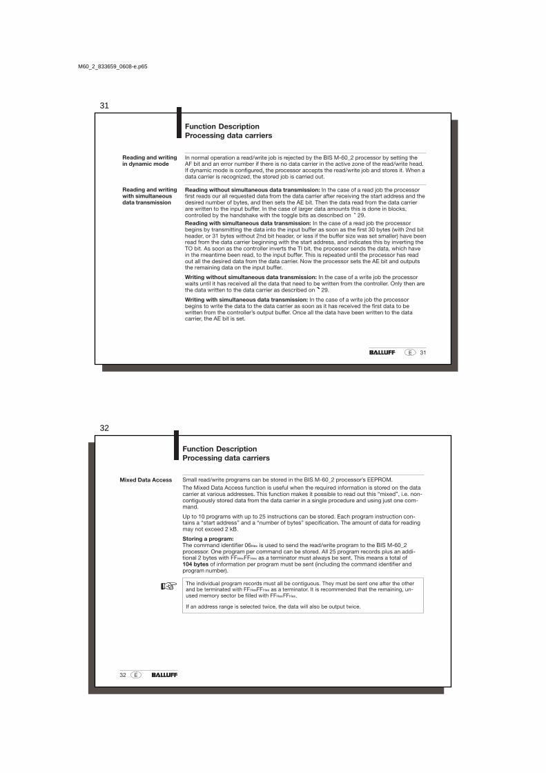
Function DescriptionOutput buffer, configuration and explanation
Bit No. 7 6 5 4 3 2 1 0
Subaddress
00Hex = Bit Header TI GR AV Bit Name
01Hex Command Designator Data
02Hex Start Address (Low Byte) or Program No. or Data
03Hex Start Address (High Byte) Data
04Hex No. of Bytes (Low Byte) Data
05Hex No. of Bytes (High Byte) Data
06Hex Data
... Data
Last Byte 2nd Bit Header (as above) Data
Sub- Bit Meaning Function Descriptionaddress Name
00Hex TI Toggle-Bit In Shows during a read action that the controller is readyBit Header for additional data.
GR Ground state Causes the BIS system to go to the ground statefor the respective read/write head.Any pending command is cancelled.
AV Command Signals the identification system that a commandfor the respective read/write head is present.
(continued next )
Description ofOutput Buffer
Please note thebasic procedure on
12 and 29...35and the exampleson pages 36...49.
M60_2_833659_0608-e.p65
16
16 E
Sub- Meaning Function Descriptionaddress
01Hex Command designator00Hex No command present01Hex Read data carrier02Hex Write to data carrier06HEX Store program in the EEPROM for the Mixed Data Access
function07HEX Store the start address for the Auto-Read function in the EEPROM12HEX Initialize the CRC_16 data check21HEX Read for Mixed Data Access function
(corresponding to the program stored in the EEPROM)22HEX Write for Mixed Data Access function
(corresponding to the program stored in the EEPROM)or: Data for writing to the data carrieror: Program data for writing to the EEPROM.
(continued next )
Function DescriptionOutput buffer, configuration and explanation
Description ofOutput Buffer(continued)
Please note thebasic procedure on
12 and 29...35and the exampleson pages 36...49.
17
17E
Function DescriptionOutput buffer, configuration and explanation
Please note thebasic procedure on
12 and 29...35and the exampleson pages 36...49.
Description ofOutput Buffer(continued)
Sub- Meaning Function Descriptionaddress
02Hex Start address Address at which reading from or writing to the data carrier begins.(Low Byte) (The Low Byte includes the address range from 0 to 255).
or: Start address Address for the Auto-Read function, starting at which the code(Low Byte) tag is to be read. The value is stored in the EEPROM. (The Low
Byte covers the address range from 0 to 255).or: Program No. Number of the program to be stored in the EEPROM in
conjunction with command ID 06Hex for Mixed Data Accessfunction (values between 01Hex and 0AHex are allowed!).
or: Program No. Number of the program stored in the EEPROM for read or writeoperations in conjunction with command ID 22Hex or 22Hex for theMixed Data Access function.
or: Data for writing to the data carrieror: Program data for writing to the EEPROM.
03Hex Start address Address for reading from or writing to the data carrier .(High Byte) (The High Byte ist reserved for future applications with larger
memory).or: Start address Address for the Auto-Read function, starting at which the code
(High Byte) tag is to be read. The value is stored in the EEPROM.(The High Byte ist reserved for future applications with largermemory).
or: Data for writing to the data carrieror: Program data for writing to the EEPROM.
(continued next )
M60_2_833659_0608-e.p65
18
18 E
Function DescriptionOutput buffer, configuration and explanation
Please note thebasic procedure on
12 and 29...35and the exampleson pages 36...49.
Description ofOutput Buffer(continued)
Sub- Meaning Function Descriptionaddress
04Hex No. of bytes Number of bytes to read or write beginning with the start address(Low Byte) (the Low Byte includes from 1 to 255 bytes).
or: Data for writing to the data carrieror: Program data for writing to the EEPROM.
05Hex No. of bytes Number of bytes to read or write beginning with the start address(High Byte) (the High Byte ist reserved for future applications with larger
memory).
or: Data for writing to the data carrier
or: Program data for writing to the EEPROM.
06Hex Data for writing to the data carrier
or: Program data for writing to the EEPROM.
... Data for writing to the data carrier
or: Program data for writing to the EEPROM.
Last byte2nd Bit header The data are valid if the 1st and 2nd bit header are identical.
or: Data for writing to the Data carrieror: Program data for writing to the EEPROM.
19
19E
Function DescriptionInput buffer, configuration and explanation
Configuration of theinput buffer for one(1) read/write head
The last byte can be arranged as a 2nd bit header through parametering (default).
Bit No. 7 6 5 4 3 2 1 0
Subaddress
00Hex = Bit Header BB HF TO IN AF AE AA CP Bit Name
01Hex Error Code or Data
02Hex Data
03Hex Data
04Hex Data
05Hex Data
06Hex Data
... Data
Last byte 2nd Bit Header (as above) or Data
Sub- Bit Meaning Function Descriptionaddress Name
00Hex BB Ready The BIS Identification System is in the Ready state.
Bit Header HF Head Error Cable break from read/write head orno read/write head connected.
TO Toggle-Bit Out for read: BIS has new/additional data ready.for write: BIS is ready to accept new/additional data.
(continued on next )
Description ofInput Buffer
Please note thebasic procedure on
12 and 29...35and the exampleson pages 36...49.
M60_2_833659_0608-e.p65
20
20 E
Function DescriptionInput buffer, configuration and explanation
Description ofInput Buffer(continued)
Sub- Bit Meaning Function Descriptionaddress Name
00Hex (continued)Bit Header IN Input If the parameter "Input IN" is 1, this bit indicates
the state of the Input.AF Command Error The command was incorrectly processed or aborted.
AE Command end The command was finished without error.
AA Command start The command was recognized and started.
CP Codetag Present Data carrier present within the active zone of theread/write head.
In addition to the CP bit, the output signal CT present is available. Thisallows you to process the presence of a data carrier directly as a hardwaresignal.
Sub- Meaning Function Descriptionaddress
01Hex Error code Error number is entered if command was incorrectly processedor aborted. Only valid with AF bit!
00Hex No error.01Hex Reading or writing not possible because no data carrier is present
in the active zone of a read/write head.02Hex Read error.03Hex Data carrier was removed from the active zone of the read/write
head while it was being read.04Hex Write error.(continued on next )
Please note thebasic procedure on
12 and 29...35and the exampleson pages 36...49.
21
21E
Function DescriptionInput buffer, configuration and explanation
Sub- Meaning Function Descriptionaddress
01Hex Error code (continued)05Hex Data carrier was removed from the active zone of the read/write
head while it was being written.07Hex AV bit is set but the command designator is missing or invalid. or: Number of bytes is 00Hex.09Hex Cable break to select read/write head, or head not connected.0CHex The EEPROM cannot be read/programmed.0DHex Communication with the read/write head.0EHex The CRC of the read data does not coincide with the CRC of
the data carrier.0FHex Contents of the 1st and 2nd bit header (1st and last bytes) of
the output buffers are not identical (2nd bit header must beserved).
20Hex Adressing of the read/write job is outside the memory range ofthe data carrier.
21Hex Function invoked which is not possible for the data carriercurrently in front of the read/write head.
or: Data Data which was read from the data carrier.
(continued next )
Description ofInput Buffer(continued)
Please note thebasic procedure on
12 and 29...35and the exampleson pages 36...49.
M60_2_833659_0608-e.p65
22
22 E
Function DescriptionInput buffer, configuration and explanation
Sub- Meaning Function Descriptionaddress
02Hex Data Data which was read from the data carrier.
... Data Data which was read from the data carrier.
Last byte2nd Bit header The data are valid if the 1st and 2nd bit headers are in
agreement.or: Data Data which was read from the data carrier.
Description ofInput Buffer(continued)
Please note thebasic procedure on
12 and 29...35and the exampleson pages 36...49.
23
23E
Function DescriptionParametering the BIS M-60_2 processor
Parameters,Overview
There are 6 user parameter bytes stored on the Profibus master that can be used to activateand deactivate various functions. Setting is done directly by linking a device to the Profibusmaster. The parameter default settings are stored in the GSD file.– CRC-16 data check:
If this function is activated, the correctness of the read or written data is ensured by aCRC-16 data check (see 8).
– Simultaneous data transmission for both read/write heads:With simultaneous data transmission shorter read/write times can be achieved dependingon the amount of data to be read/written and the type of controller.
– Dynamic operation on read/write head 1 or 2:If dynamic operation is parametered, a read/write job can be sent even though there is noData carrier in the active zone of the head. As soon as a Data carrier passes by the head,the command is immediately carried out.
– "Auto-Read” for read/write head 1 or 2:If this function is activated, the processor reads out the first (max. 31) bytes from the Datacarrier starting at a defined start address as soon as the tag enters the active zone of theread/write head. The start address must first have been stored in the processor’s EEPROMwith the command ID 07Hex.
– 2nd bit header at end of in- and output buffer:The 2nd bit header (factory setting) prevents data from being accepted by the bus as longas it is not fully updated.
– Display state of the digital input in the bit header of the input buffer:If this function is activated, the IN-bit displays the state of the digital input of the processor:IN = 0 → digital input low; IN = 1 → digital input highPlease note the
basic procedure on 12 and 29...35
and the exampleson pages 36...49.
M60_2_833659_0608-e.p65
24
24 E
Function DescriptionParametering the BIS M-60_2 processor
Parameters,Overview(continued)
– Reset BIS M-60_2 processor through the digital input:If this function is activated, the processor is reset when the digital input is set to high.
– Output data carrier model and serial number:If this function is activated, at CT Present the data carrier model and serial number are out-put.
If this function is activated, no read data are output at CT Present for models BIS M-1_ _-02/Ldata carriers.
Please note thebasic procedure on
12 and 29...35and the exampleson pages 36...49.
☞
25
25E
Parametering BytesUser-Parameter Bytes
For parametering all 6 bytes must always be transferred in Hex. Only the bits mentionedmay be changed. No guaranty will be given for the proper functioning of theBIS M-60_2 if any of the other bits are changed.
The default values (factory setting) for the 6 bytes are:
bit 4 bit 1...8 bit 7 bit 1 bit 4 bit 1...8 bit 5 bit 5 bit 8 bit 2 bit 5
bit 8
The bits which serve for parametering have the following functions:
1st byte, bit 5 Activate CRC_16 data checking
2nd byte, bit 5 Dynamic mode on read/write head 1(for effects on read/write times, see 50)
2nd byte, bit 4 Activate Auto-Read function starting at specified address afterCT present for Head 1 (the number of bytes read depends on theselected buffer size minus bit headers for Head 1)
3nd byte, bit 1...8 Select data-carrier model for processing:00HEX: All data-carrier models01HEX: Model BIS M-1_ _-02/L
Function DescriptionParametering, Parametering Bytes
Bit state: 0 = no1 = yes
These are used forconfiguration:
Having the followingfunctions:
Please note thebasic procedure on
12 and 29...35and the exampleson pages 36...49.
M60_2_833659_0608-e.p65
26
26 E
4th byte, bit 8 Arrange a 2nd bit header at the end of the input and output buffers
If this function is selected, then the minimum size of both buffers is 4 words (8 bytes) each.
4th byte, bit 7, Display state of the digital input in the bit header of the input buffers:0 = no1 = yes Input is Low: "IN" in the bit header of the input buffers = 0.
Input is High: "IN" in the bit header of the input buffers = 1.
4th byte, bit 2, Reset the BIS M-60_2 processor through the digital input:0 = no1 = yes Input is Low: Do not reset.
Input is High: Reset.
4th byte, bit 1, Output data-carrier model and serial number at CT present:0 = no AT CT present the first data carrier data are output on Profibus.1 = yes AT CT present the data carrier model and serial number are output on
Profibus.
5th byte, bit 8 Activate simultaneous data transmission for both read/write heads
5th byte, bit 5 Dynamic mode on read/write head 2(for effects on read/write times, see 50)
5th byte, bit 4 Activate Auto-Read function for Head 2 starting at specified address afterCT present (the number of bytes read depends on the selected buffer sizeminus bit headers for Head 2)
Parametering BytesUser-Parameter Bytes(continued)
Function DescriptionParametering, Parametering Bytes
Bit state: 0 = no1 = yes
Please note thebasic procedure on
12 and 29...35and the exampleson pages 36...49.
27
27E
6th byte, bit 1...6 No. of bytes in input and output buffer which shall be used forread/write head 1, see example on 14.
The specification for the input and output buffer on the Master applies to both read/writeheads, i.e. this buffer must be divided for both heads. The specification is done in Hex formatand must be in a range between 02Hex and 80Hex (128 dec.).
If only one read/write head (Head 1) will be used, you may enter the same value here as for thetotal buffer size. An entry of less than 2 bytes results in an undefined state.
Please note the basic procedure on 12 and 29...35 and the examples on pages 36...49.
Parametering BytesUser-Parameter Bytes(continued)
Function DescriptionParametering, Parametering Bytes
☞
M60_2_833659_0608-e.p65
28
28 E
Data-carrier modelsBIS M-1_ _-02/L
CT present
Model BIS M-1_ _-02/L data carriers have a memory capacity of 752 bytes of user data.These data can be read or programmed. These data carriers also have a unique, 4-byte serialnumber, which is read-only.The data carrier also contains additional memory ranges for configuration and protected data.These areas cannot be processed using the BIS M-60_2 processor.
At CT Present the first user data are read from the data carrier and stored in the Profibus inputbuffer (see 30). If the “Output data-carrier model and serial number at CT present” functionis enabled, model 01Hex is output in Byte 1 of the input buffer and then the 4 bytes represent-ing the unique serial number.
The full command set of the BIS M-60_2 processor can be used with model BIS M-1_ _02/Ldata carriers.
When using model BIS M-1_ _-02/L data carriers, the device parameterizing depends mainlyon the number of bytes to be read and programmed per head.
Please refer to 13ff and 23ff.
Functions
Device parameters
☞
Data carrierBIS M-1_ _-02/L
29
29E
Function DescriptionProcessing data carriers
Reading and writing To carry out a read or write job, the data carrier must be located in the active zone of the read/write head.
Read/write commands can be executed only with model BIS M-1_ _-02/L data carriers.
A read/write job has the following sequence (see examples on 36ff):
1. The host sends to the output buffer:– the command designator to subaddress 01Hex,– the start address for reading or writing to subaddress 02HEX/03HEX,– the number of bytes for reading or writing to subaddress 04HEX/05HEX,– and sets the AV bit in the bit header to high.
2. The processor:– takes the request (AA in the bit header of the input buffer to high),– begins to transport the data;
read = from data carrier to input buffer,write = from output buffer to data carrier.(Larger data quantities are sent in blocksblock size with 2nd bit header = buffer size - 2,block size without 2nd bit header = buffer size - 1).The toggle bits in the two bit headers are used as a kind of handshaking between thehost and the BIS M-60_2 processor.
3. The processor has processed the command correctly (AE bit in the bit header of the inputbuffer). If an error occurred during execution of the command, an error number will bewritten to subaddress 01Hex of the input buffer and the AF bit in the bit header of the inputbuffer will be set.
☞
M60_2_833659_0608-e.p65
30
30 E
Start address forAuto-Read
Function DescriptionProcessing data carriers
Codetag Present(CP bit)
As soon as the data carrier enters the active one of the read/write head, the processor indi-cates this by setting the CP bit (Codetag Present).
To accelerate the reading of small amounts of data, the ID system makes the first bytes of thedata carrier available in the input buffer of the respective read/write head as soon as the tag isdetected. The number of bytes sent corresponds to the configured buffer size – 1 byte (2 bytesfor 2nd bit header).
If the parameter “Output data-carrier model and serial number at CT Present” is set, thedata-carrier model and unique serial number are output instead of the read data.
The data are only valid after the rising edge of the CP bit in the bit header of the input buffer.They remain valid until the falling edge of the CP bit, or until the controller issues a new job.
If the Auto-Read function is activated, the data are read starting with a specified start addressas soon as the data carrier is recognized. The rising edge of the CP bit is used to providethese data in the input buffer. The start address must be specified for each head usingcommand identifier 07Hex the start addresses may be different. The number of bytes read isdetermined by the selected size of the input buffer, which is distributed over both heads when2 are used.
☞
31
31E
Function DescriptionProcessing data carriers
Reading and writingin dynamic mode
In normal operation a read/write job is rejected by the BIS M-60_2 processor by setting theAF bit and an error number if there is no data carrier in the active zone of the read/write head.If dynamic mode is configured, the processor accepts the read/write job and stores it. When adata carrier is recognized, the stored job is carried out.
Reading without simultaneous data transmission: In the case of a read job the processorfirst reads our all requested data from the data carrier after receiving the start address and thedesired number of bytes, and then sets the AE bit. Then the data read from the data carrierare written to the input buffer. In the case of larger data amounts this is done in blocks,controlled by the handshake with the toggle bits as described on 29.Reading with simultaneous data transmission: In the case of a read job the processorbegins by transmitting the data into the input buffer as soon as the first 30 bytes (with 2nd bitheader, or 31 bytes without 2nd bit header, or less if the buffer size was set smaller) have beenread from the data carrier beginning with the start address, and indicates this by inverting theTO bit. As soon as the controller inverts the TI bit, the processor sends the data, which havein the meantime been read, to the input buffer. This is repeated until the processor has readout all the desired data from the data carrier. Now the processor sets the AE bit and outputsthe remaining data on the input buffer.
Writing without simultaneous data transmission: In the case of a write job the processorwaits until it has received all the data that need to be written from the controller. Only then arethe data written to the data carrier as described on 29.
Writing with simultaneous data transmission: In the case of a write job the processorbegins to write the data to the data carrier as soon as it has received the first data to bewritten from the controller’s output buffer. Once all the data have been written to the datacarrier, the AE bit is set.
Reading and writingwith simultaneousdata transmission
M60_2_833659_0608-e.p65
32
32 E
Mixed Data Access
Function DescriptionProcessing data carriers
Small read/write programs can be stored in the BIS M-60_2 processor’s EEPROM.The Mixed Data Access function is useful when the required information is stored on the datacarrier at various addresses. This function makes it possible to read out this “mixed”, i.e. non-contiguously stored data from the data carrier in a single procedure and using just one com-mand.
Up to 10 programs with up to 25 instructions can be stored. Each program instruction con-tains a “start address” and a “number of bytes” specification. The amount of data for readingmay not exceed 2 kB.
Storing a program:The command identifier 06Hex is used to send the read/write program to the BIS M-60_2processor. One program per command can be stored. All 25 program records plus an addi-tional 2 bytes with FFHexFFHex as a terminator must always be sent. This means a total of104 bytes of information per program must be sent (including the command identifier andprogram number).
The individual program records must all be contiguous. They must be sent one after the otherand be terminated with FFHexFFHex as a terminator. It is recommended that the remaining, un-used memory sector be filled with FFHexFFHex.
If an address range is selected twice, the data will also be output twice.
☞
33
33E
Mixed Data Access(continued)
The following shows the structure of a program:
Program structure Subaddress Value Range
Command designator 01Hex 06Hex
1. Program recordProgram number 02Hex 01Hex 01Hex to 0AHex
1st data record:Start address Low Byte 03Hex
Start address High Byte 04Hex
Number of bytes Low Byte 05Hex
Number of bytes High Byte 06Hex
2nd data record:...
25th data record:Start address Low Byte 03Hex
Start address High Byte 04Hex
Number of bytes Low Byte 05Hex
Number of bytes High Byte 06Hex
Terminator FFHex FFHex
To store a second program, repeat this process.
The procedure for writing these settings to the EEPROM is described in the 7th example on 44...46.
Replacing the EEPROM is described on 57 for BIS M-6002 and on 67 for BIS M-6022.
Function DescriptionProcessing data carriers
M60_2_833659_0608-e.p65
34
34 E
Function DescriptionProcessing data carriers
Read from datacarrier, with programMixed Data Access
Write to data carrier,with program MixedData Access
The command identifier 21Hex can be used to read out the program records stored in theprogram from the data carrier. The user must document exactly which data are to be readfrom where and with what number of bytes for the respective program (see example 8 on 47)
The command identifier 22Hex can be used to write the program records stored in the programto the data carrier. The user must document exactly which data are to be written from whereand with what number of bytes for the respective program (see example 9 on 48)
To be able to use the CRC_16 check, the data carrier must first be initialized with thecommand identifier 12Hex (see 36). The CRC_16 initialization is used like a normal write job.The latter is rejected (with an error message) if the processor recognizes that the data carrierdoes not contain the correct CRC_16 checksum. Data carriers as shipped from the factory (alldata are 0) can immediately be written with CRC-checked data.If CRC_16 data checking is activated, a special error message is output to the interfacewhenever a CRC_16 error is detected.
If the error message is not caused by a failed write request, it may be assumed that one ormore memory cells on the data carrier is defective. That data carrier must then be replaced.
If the CRC error is however due to a failed write request, you must reinitialize the data carrierin order to continue using it.
CRC_16 initialization
35
35E
Function DescriptionProcessing data carriers
Data carrier model Memory capacity Usable bytes with CRC_16
BIS M-1_ _-02/L = 752 bytes 658 bytes
If CRC_16 was parameterized and a data carrier is recognized whose CRC_16 checksum isincorrect, the read data are not output and the CP bit in the iput bit header is not set. The CTpresent LED comes on and the digital output is set - the data carrier can be processed usingthe initialization command (12Hex).
The checksum is written to the data carrier as a 2-byte datum for each CRC block (corre-sponds to 16 bytes). 2 bytes are used (lost) for each CRC block, i.e., the CRC block containsonly 14 bytes of user data. This means that the actual usable number of bytes is reduced:
CRC_16 andCodetag Present
CRC_16 andmemory capacity
M60_2_833659_0608-e.p65
36
36 E
Example No. 1
For configuring withdouble bit headerand 8-byte buffersize!
... To be continueduntil the completememory range iswritten. See next .
Function DescriptionExamples for protocol sequence
Initializing the data carrier for the CRC_16 data checkingThe processing of this command is similar to a write command. Start address and number ofbytes have to correspond to the maximum number of data to be used.In this example the complete memory range of a data carrier with 752 bytes shall be used(BIS M-1_ _-02/L). Because 2 bytes are used for the CRC only 658 bytes can be used as databytes, hence: start address = 0, number of bytes = 658.
5.) Process subaddresses of the output buffer:
BIS M-60_2 Identification System:
2.) Process subaddresses of the input buffer in theorder shown:
3.) Process subaddresses of the output buffer: 4.) Process subaddresses of the output buffer:
6.) Process subaddresses of the output buffer:
Host:
1.) Process subaddresses of the output buffer in theorder shown:
00Hex/07Hex Set AA-Bit, invert TO-Bit01Hex Command designator 12Hex
02Hex Start address 00Hex
03Hex Start address 00Hex
04Hex No. of bytes A8Hex
05Hex No. of bytes 00Hex
00Hex/07Hex Set AV-Bit
01...06Hex Enter first 6 bytes of data
00Hex/07Hex Invert TI-Bit
01...06Hex Enter the second 6 data bytes
00Hex/07Hex Invert TI-Bit
01...06Hex Copy first 6 data bytes
Process subaddress of the input buffer:
00Hex/07Hex Invert TO-Bit
01...06Hex Copy second 6 data bytes
Process subaddress of the input buffer:
00Hex/07Hex Invert TO-Bit
37
37E
Example No. 1(continued)
For configuring withdouble bit headerand 8-byte buffersize!
Function DescriptionExamples for protocol sequence
Host: BIS M-60_2 Identification System:
9.) Process subaddresses of the output buffer: 10.)Process subaddresses of the input buffer:
7.) Process subaddresses of the output buffer: 8.) Process subaddresses of the output buffer:
01...06Hex Enter the remaining data byte
00Hex/07Hex Invert TI-Bit
00Hex/07Hex Reset AV-Bit
01...06Hex Copy the remaining data byte
Process subaddress of the input buffer:
00Hex/07Hex Set AE-Bit
00Hex/07Hex Reset AA-Bit and AE-Bit
M60_2_833659_0608-e.p65
38
38 E
Function DescriptionExamples for protocol sequence
Read 17 bytes starting at data carrier address 10 (data carrier type BIS M-1_ _-02/L):Example No. 2
For configuring withdouble bit headerand 8-byte buffersize!
7.) Process subaddresses of the input buffer: 8.) Process subaddresses of the input buffer:
BIS M-60_2 Identification System:
2.) Process subaddresses of the input buffer in theorder shown:
3.) Process subaddresses of the input buffer: 4.) Process subaddresses of the input buffer:
6.) Process subaddresses of the input buffer:5.) Process subaddresses of the input buffer:
Host:
1.) Process subaddresses of the output buffer in theorder shown:
01Hex Command designator 01Hex
02Hex Start address Low Byte 0AHex
03Hex Start address High Byte 00Hex
04Hex No. of bytes Low Byte 11Hex
05Hex No. of bytes High Byte 00Hex
00Hex/07Hex Set AV-Bit
00Hex/07Hex Set AA-Bit
01...06Hex Enter first 6 bytes of data
00Hex/07Hex Set AE-Bit
01...06Hex Copy first 6 data bytes
Process subaddress of the output buffer:
00Hex/07Hex Invert TI-Bit
01...06Hex Enter the second 6 data bytes
00Hex/07Hex Invert TO-Bit
01...06Hex Copy second 6 data bytes
Process subaddress of the output buffer:
00Hex/07Hex Invert TI-Bit
01...05Hex Enter the remaining 5 data bytes
00Hex/07Hex Invert TO-Bit
01...05Hex Copy the remaining 5 data bytes
Process subaddress of the output buffer:
00Hex/07Hex Reset AV-Bit
00Hex/07Hex Reset AA-Bit and AE-Bit
39
39E
Function DescriptionExamples for protocol sequence
Read 17 bytes starting at data carrier address 10, with simultaneous data transmission(data carrier type BIS M-1_ _-02/L):While the read job is being carried out and as soon as the input buffer is filled, the first dataare sent. The AE bit is not set until the “Read” operation is completed by the processor.
The reply “Job End” = AE bit is reliably set no later than before the last data are sent. Theexact time depends on the requested data amount, the input buffer size and the timing of thecontroller. This is indicated in the following by the note Set AE-Bit (in italics).
01Hex Command designator 01Hex
02Hex Start address Low Byte 0AHex
03Hex Start address High Byte 00Hex
04Hex No. of bytes Low Byte 11Hex
05Hex No. of bytes High Byte 00Hex
00Hex/07Hex Set AV-Bit
00Hex/07Hex Set AA-Bit
01...06Hex Enter first 6 bytes of data
00Hex/07Hex Invert TO-Bit
00Hex/07Hex Set AE-Bit
01...06Hex Enter the second 6 data bytes
00Hex/07Hex Invert TO-Bit
00Hex/07Hex Set AE-Bit
01...06Hex Copy first 6 data bytes
00Hex/07Hex Invert TI-Bit
Example No. 3like 2nd example butwith simultaneousdata transmission
For configuring withdouble bit headerand 8-byte buffersize!
Continued on next .
BIS M-60_2 Identification System:
2.) Process subaddresses of the input buffer in theorder shown:
Host:
1.) Process subaddresses of the output buffer in theorder shown:
3.) Process subaddresses of the input buffer: 4.) Process subaddresses of the input buffer:
M60_2_833659_0608-e.p65
40
40 E
Function DescriptionExamples for protocol sequence
Host: BIS M-60_2 Identification System:
01...05Hex Enter the remaining 5 data bytes
00Hex/07Hex Invert TO-Bit
00Hex/07Hex Set AE-Bit
Example No. 3(continued)
like 2nd example butwith simultaneousdata transmission
For configuring withdouble bit headerand 8-byte buffersize!
7.) Process subaddresses of the input buffer: 8.) Process subaddresses of the input buffer:
6.) Process subaddresses of the input buffer:5.) Process subaddresses of the input buffer:
01...06Hex Copy second 6 data bytes
Process subaddress of the output buffer:
00Hex/07Hex Invert TI-Bit
01...05Hex Copy the remaining 5 data bytes
Process subaddress of the output buffer:
00Hex/07Hex Reset AV-Bit
00Hex/07Hex Reset AA-Bit and AE-Bit
41
41E
Function DescriptionExamples for protocol sequence
Example No. 4
For configuring withdouble bit headerand 8-byte buffersize!
Read 30 bytes starting at data carrier address 10 with read error(data carrier type BIS M-1_ _-02/L):
Host:
1.) Process subaddresses of the output buffer in theorder shown:
BIS M-60_2 Identification System:
2.) Process subaddresses of the input buffer in theorder shown:
If an error occurs right away:
3.) Process subaddress of the input buffer: 4.) Process subaddresses of the input buffer:
01Hex Command designator 01Hex
02Hex Start address Low Byte 0AHex
03Hex Start address High Byte 00Hex
04Hex No. of bytes Low Byte 1EHex
05Hex No. of bytes High Byte 00Hex
00Hex/07Hex Set AV-Bit
00Hex/07Hex Set AA-Bit
01Hex Enter error number
00Hex/07Hex Set AF-Bit
01Hex Copy error number
Process subaddress of the output buffer:
00Hex/07Hex Reset AV-Bit
00Hex/07Hex Reset AA-Bit and AF-Bit
M60_2_833659_0608-e.p65
42
42 E
Function DescriptionExamples for protocol sequence
Example No. 5
For configuring withdouble bit headerand 8-byte buffersize!
Write 16 bytes starting at data carrier address 20 (data carrier type BIS M-1_ _-021/L):
Host:
1.) Process subaddresses of the output buffer in theorder shown:
BIS M-60_2 Identification System:
2.) Process subaddresses of the input buffer in theorder shown:
3.) Process subaddresses of the output buffer: 4.) Process subaddresses of the output buffer:
9.) Process subaddresses of the output buffer: 10.)Process subaddresses of the input buffer:
5.) Process subaddresses of the output buffer: 6.) Process subaddresses of the output buffer:
7.) Process subaddresses of the output buffer: 8.) Process subaddresses of the output buffer:
01Hex Command designator 02Hex
02Hex/03Hex Start address 14Hex / 00Hex
04Hex/05Hex No. of bytes 10Hex / 00Hex
00Hex/07Hex Set AV-Bit
00Hex/07Hex Set AA-Bit, invert TO-Bit
01...06Hex Enter the first 6 data bytes
00Hex/07Hex Invert TI-Bit
01...06Hex Copy first 6 data bytes
Process subaddress of the input buffer:
00Hex/07Hex Invert TO-Bit
01...06Hex Enter the second 6 data bytes
00Hex/07Hex Invert TI-Bit
01...06Hex Copy second 6 data bytes
Process subaddress of the input buffer:
00Hex/07Hex Invert TO-Bit
01...04Hex Enter the remaining 4 data bytes
00Hex/07Hex Invert TI-Bit
01...04Hex Copy the remaining 4 data bytes
Process subaddress of the input buffer:
00Hex/07Hex Set AE-Bit
00Hex/07Hex Reset AV-Bit 00Hex/07Hex Reset AA-Bit and AE-Bit
43
43E
Example No. 6Address assignmentfor the Auto-Readfunction
For configuring withdouble bit headerand 8-byte buffersize!
Programming start address 75:
01Hex Command designator 07Hex
02Hex Start address Low Byte 4BHex
03Hex Start address High Byte 00Hex
00Hex/07Hex Set AV-Bit
00Hex/07Hex Set AA-Bit and AE-Bit
To ensure correct data output, use command identifier 07Hex for each distributed buffer Head 1and/or Head 2.
If the Auto-Read function is not activated, the processor runs in standard mode and sendsstarting with data carrier address 0 until the buffer is filled.
☞
Host:
1.) Process subaddresses of the output buffer in theorder shown:
BIS M-60_2 Identification System:
2.) Process subaddresses of the input buffer:
3.) Process subaddresses of the output buffer: 4.) Process subaddresses of the input buffer:
00Hex/07Hex Reset AV-Bit 00Hex/07Hex Reset AA-Bit and AE-Bit
Function DescriptionExamples for protocol sequence
M60_2_833659_0608-e.p65
44
44 E
Function DescriptionExamples for protocol sequence
Example No. 7Store Mixed DataAccess program
For configuring withdouble bit headerand 8-byte buffersize!
Storing a program for reading out 3 data records:1st data record Start address 5 Number of bytes 72nd data record Start address 75 Number of bytes 33rd data record Start address 112 Number of bytes 17
Total number of bytes exchanged in the operation: 27 bytesAll 104 bytes are written for the programming.
Host:
1.) Process subaddresses of the output buffer in theorder shown:
BIS M-60_2 Identification System:
2.) Process subaddresses of the input buffer:
01Hex Command designator 06Hex
02Hex Program number 01Hex
00Hex/07Hex Set AV-Bit
00Hex/07Hex Set AA-Bit, invert TO-Bit
3.) Process subaddresses of the output buffer: 4.) Process subaddresses of the input buffer:
01Hex 1st start address (Low Byte) 05Hex
02Hex (High Byte) 00Hex
03Hex 1st number ofbytes
(Low Byte) 07Hex
04Hex (High Byte) 00Hex
05Hex 2nd start address (Low Byte) 4BHex
06Hex (High Byte) 00Hex
00Hex/07Hex Invert TI-Bit
00Hex/07Hex Invert TO-Bit
Continued on next .
45
45E
Function DescriptionExamples for protocol sequence
Host: BIS M-60_2 Identification System:Example No. 7Store Mixed DataAccess program(continued)
For configuring withdouble bit headerand 8-byte buffersize!
5.) Process subaddresses of the output buffer: 6.) Process subaddresses of the input buffer:
01Hex
02Hex
2nd number ofbytes
(Low Byte) 03Hex
(High Byte) 00Hex
03Hex 3rd start address (Low Byte) 70Hex
04Hex (High Byte) 00Hex
05Hex 3rd number ofbytes
(Low Byte) 11Hex
06Hex (High Byte) 00Hex
00Hex/07Hex Invert TI-Bit
00Hex/07Hex Invert TO-Bit
7.) Process subaddresses of the output buffer: 8.) Process subaddresses of the input buffer:
01Hex/02Hex Terminator FFHex/FFHex
03Hex/04Hex (not used) FFHex/FFHex
05Hex/06Hex (not used) FFHex/FFHex
00Hex/07Hex Invert TI-Bit
00Hex/07Hex Invert TO-Bit
Fill all unused start addresses and number of bytes with FFHex! Continued on next .
M60_2_833659_0608-e.p65
46
46 E
Function DescriptionExamples for protocol sequence
Host: BIS M-60_2 Identification System:
00Hex/07Hex Reset AV-Bit 00Hex/07Hex Reset AA-Bit and AE-Bit
9.) Process subaddresses of the output buffer: 10.)Process subaddresses of the input buffer:
01Hex/02Hex (not used) FFHex/FFHex
03Hex/04Hex (not used) FFHex/FFHex
05Hex/06Hex (not used) FFHex/FFHex
00Hex/07Hex Invert TI-Bit
00Hex/07Hex Set AE-Bit
11.)Process subaddresses of the output buffer: 12.)Process subaddresses of the input buffer:
We recommend that you carefully document which parameters are used for start addresses andnumber of bytes for writing/reading the desired data records.
The data are sequenced in the exact order specified in the program.
☞
Example No. 7Store Mixed DataAccess program(continued)
For configuring withdouble bit headerand 8-byte buffersize!
47
47E
Function DescriptionExamples for protocol sequence
Example No. 8Use Mixed DataAccess program
For configuring withdouble bit headerand 8-byte buffersize!
Read data carrier using Program No. 1 (data carrier type BIS M-1_ _-02/L):
01Hex Command designator 21Hex
02Hex Program number 01Hex
00Hex/07Hex Set AV-Bit
00Hex/07Hex Set AA-Bit
01...06Hex Enter first 6 bytes of data
00Hex/07Hex Set AE-Bit
01...06Hex Enter the second 6 data bytes
00Hex/07Hex Invert TO-Bit
01...06Hex Copy first 6 data bytes
00Hex/07Hex Invert TI-Bit
... A total of 27 bytes of data are exchanged.For the remainder of the procedure, see Example 2 on 38.
Dynamic mode is turned off while the Mixed Data Access program is being run.☞
Host:
1.) Process subaddresses of the output buffer in theorder shown:
BIS M-60_2 Identification System:
2.) Process subaddresses of the input buffer in theorder shown:
3.) Process subaddresses of the input buffer: 4.) Process subaddresses of the output buffer:
M60_2_833659_0608-e.p65
48
48 E
Function DescriptionExamples for protocol sequence
Example No. 9Use Mixed DataAccess program
For configuring withdouble bit headerand 8-byte buffersize!
Write data carrier using Program No. 1 (data carrier type BIS M-1_ _-02/L):
01Hex Command designator 22Hex
02Hex Program number 01Hex
00Hex/07Hex Set AV-Bit
... A total of 27 bytes of data are exchanged.For the remainder of the procedure, see Example 5 on 42.
Dynamic mode is turned off while the Mixed Data Access program is being run.
Host:
1.) Process subaddresses of the output buffer in theorder shown:
BIS M-60_2 Identification System:
2.) Process subaddresses of the input buffer in theorder shown:
3.) Process subaddresses of the output buffer: 4.) Process subaddresses of the output buffer:
00Hex/07Hex Set AA-Bit, invert TO-Bit
01...06Hex Enter first 6 bytes of data
00Hex/07Hex Invert TI-Bit
01...06Hex Copy first 6 data bytes
Process subaddress of the input buffer:
00Hex/07Hex Invert TO-Bit
☞
49
49E
Function DescriptionExamples for protocol sequence
Example No. 10 Put the relevant read/write head into ground state:Both read/write heads can be independently set to the ground state.
Host:
1.) Process subaddresses of the output buffer:
BIS M-60_2 Identification System:
2.) Go to ground state;Process subaddresses of the input buffer:
3.) Process subaddresses of the output buffer: 4.) Process subaddresses of the input buffer:
00Hex/07Hex Set GR-Bit 00Hex/07Hex Reset BB-Bit
00Hex/07Hex Reset GR-Bit 00Hex/07Hex Set BB-Bit
M60_2_833659_0608-e.p65
50
50 E
Read/Write Times
Read times
All data are typical values. Deviations are possible depending on the application and combinationof read/write head and data carrier!The data apply to static operation, no CRC_16 data checking.
Write times
Data carrier BIS M-1_ _ with each 16 bytes/block
Time for data carrier recognition/serial ID < 20 ms
Read bytes 0 to 15 < 15 ms
For each additional 16 bytesadd another < 10 ms
Data carrier BIS M-1_ _ with each 16 bytes/block
Time for data carrier recognition/serial ID < 20 ms
Write bytes 0 to 15 < 45 ms
For each additional 16 bytesadd another < 35 ms
☞
51
51E
Function displayson BIS M-60_2
The BIS M-60_2 uses the three side-mounted LED's to indicate important conditions of theidentification system.Status LED Meaning
Ready / red Supply voltage OK; no hardware error,Bus active however, bus not active.
green Supply voltage / hardware OK,bus active.
CT1 Present / green Data carrier read/write-ready at read/write head 1.operating yellow Read/write command at read/write head 1 in
process.yellow flashes Cable break to read/write head or not connected.[f ≈ 2 Hz]yellow flashes faster Communication with R/W Head 1 is faulty[f ≈ 4 Hz] or R/W Head 1 is defective.off No data carrier in read/write range of
read/write head 1.
CT2 Present / green Data carrier read/write-ready at read/write head 2.operating yellow Read/write command at read/write head 2 in
process.yellow flashes Cable break to read/write head or not connected.[f ≈ 2 Hz]yellow flashes faster Communication with R/W Head 2 is faulty[f ≈ 4 Hz] or R/W Head 2 is defective.off No data carrier in read/write range of
read/write head 2.
If all three LED's are synchronously flashing, it means a hardware error. Return the unit to the factory.
LED Display
M60_2_833659_0608-e.p65
52
52 E
BIS M-6002Mounting the Processor
The processor is attached using 4 M4 screws.Mounting theBIS M-6002processor
X1 X2 X3
Head1Head2
12.5
12
.8
16
.8
15
0
90
4.3
71
.6
45.5
~9
.5
~1
9.6
18.5
21.5
82
BIS M-6002dimensions
53
53E
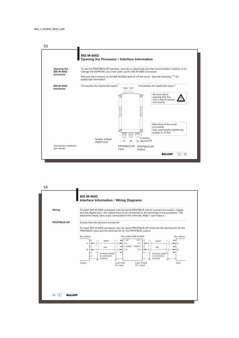
BIS M-6002Opening the Processor / Interface Information
X1 X2 X3
Head1Head2BIS M-6002interfaces
PROFIBUS-DPOutput
PROFIBUS-DPInput
Connection locationsand names
Supply voltagedigital input
Functionground FE
To set the PROFIBUS-DP address, activate or deactivate the internal termination resistor, or tochange the EEPROM, you must open up the BIS M-6002 processor.
Remove the 4 screws on the BIS M-6002 and lift off the cover. See the following foradditional information.
Connection for read/write head 2 Connection for read/write head 1
Opening theBIS M-6002processor
Be sure beforeopening that theunit is disconnectedfrom power.
Mounting of the cover(4 screws),max. permissible tighteningtorque: 0.15 Nm
M60_2_833659_0608-e.p65
54
54 E
BIS M-6002Interface Information / Wiring Diagrams
Ensure that the device is turned off.
To insert BIS M-6002 processor into the serial PROFIBUS-DP, there are the terminal X2 for thePROFIBUS input and the terminal X3 for the PROFIBUS output.
...
1
2
3
4
1
2
3
4
A
B
VP
DGND
A
B
VP
DGND
A
B
A
B
Wiring To insert BIS M-6002 processor into the serial PROFIBUS and to connect the supply voltageand the digital input, the cables have to be connected to the terminals of the processor. Theread/write heads have to be connected to the terminals Head 1 and Head 2.
Bus station BIS M-6002Bus station Bus station
5-pin femaleX3, output
5-pin maleX2, input
Output Input
Connect shieldto connectorhousing
Connect shieldto connectorhousing
green
red red
green
PROFIBUS-DP
55
55E
BIS M-6002Interface Information / Wiring Diagrams
The last bus module must terminate the bus with a resistor. In the case of the BIS M-6002,this can be realized in two different ways:
1. In the device by closing the switch S2(factory standard is open)Note: Output terminal must be closedoff with a screw cover in order tomaintain the enclosure rating.
2. Outside the device in a connector to socket X3. In this case the signal VP (pin 1) andDGND (pin 3) should be brought out in order to connect the external resistor to the poten-tial.Note: In this case S2 has to be open!
S2 Terminating resistor
closed activeopen passive
PROFIBUS-DPTerminating resistor
M60_2_833659_0608-e.p65
56
56 E
Wiring diagram forBIS M-6002processor
BIS M-6002Interface Information / Wiring Diagrams
X1 X2 X3
Head1Head2
PROFIBUS-DP
Supplyvoltage,digital input
Functionground FE
1 2
3
5
4
X1, supply voltage, digital input
X2, PROFIBUS-input (male)
1 2
3
5
4
n.c. = do notconnect
X3, PROFIBUS-output (female)
2 1
4
5
3 Pin Function
1 VP
2 A
3 DGND
4 B
5 n.c.
Pin Function
1 +Vs
2 –IN
3 –Vs
4 +IN
5 n.c.
Connection for Read/Write Head 2
The function-ground connector FE should beconnected to earth directly or through a RCcombination depending on the system (poten-tial counterpoise).When connecting the bus leads, make surethat the shield has proper connection to con-nector housing.
Connection forRead/Write Head 1
Terminal location anddesignation
57
57E
Changing theEEPROM in theBIS M-6002processor
Location of theEEPROM
BIS M-6002Changing the EEPROM
To replace the EEPROM, open up the processor as described on 53.
Be sure before opening that the unit is discon-nected from power.
To avoid damaging the EEPROM, please ob-serve the requirements for handling electrostati-cally sensitive components.
The EEPROM is replaced by unplugging andplugging back into the socket.
X1 X2 X3
Head1Head2
1
on
2
4
3
onon
on
6
7
onon
5
on
8
on
onon on
Head 1Head 2
S1
13 246 578911121416 15 13 10
S2
1719 18
M60_2_833659_0608-e.p65
58
58 E
Dimensions,Weight
Housing PlasticDimensions approx. 179 x 90 x 45,5 mmWeight approx. 500 g
Ambient temperature 0 °C to + 60 °C
Enclosure rating IP 65 (when connected)
Integral connector X1 for VS, IN 5-pin (male)Integral connector X2 for PROFIBUS-DP Input 5-pin (male)Integral connector X3 for PROFIBUS-DP Output 5-pin (female)
Supply voltage VS, input DC 24 V ± 20 %Ripple ≤ 10 %Current draw ≤ 400 mAPROFIBUS-DP slave Terminal block, electrically isolated
Digital Input (+IN, –IN) Optocoupler isolatedControl voltage active 4 V to 40 VControl voltage inactive 1.5 V to –40 VInput current at 24 V 11 mADelay time, typ. 5 ms
Read/Write Head 2 x connectors 8-pin (female)for all read/write heads BIS M-3_ _with 8-pin connector (male)
OperatingConditions
Connections
Enclosure Rating
ElectricalConnections
BIS M-6002Technical Data
59
59E
BIS operating messages:Ready / Bus active LED red / greenCT1 Present / operating LED green / yellowCT2 Present / operating LED green / yellow
BIS M-6002Technical Data
Function displays
The CE-Mark is your assurance that our products are in conformance with theEC-Guideline
89/336/EEC (EMC-Guideline)
and the EMC Law. Testing in our EMC Laboratory, which is accredited by the DATech forTesting of Electromagnetic Compatibility, has confirmed that Balluff products meet theEMC requirements of the Generic Standard
EN 61000-6-4 (Emission) and EN 61000-6-2 (Noise Immunity).
M60_2_833659_0608-e.p65
60
60 E
Balluff Identification System
Type M Read/Write System
Hardware-Typ6002 = plastic housing, PROFIBUS-DP
Software-Typ019 = PROFIBUS-DP
Read/Write Head050 = with two connections for external read/write heads BIS M-3_ _
Interface03 = BUS versions
User ConnectionST11 = Connector version X1, X2, X3 (2× male 5-pin, 1× female 5-pin)
Ordering Code
BIS M-6002Ordering Information
BIS M-6002-019-050-03-ST11
61
61E
Type Ordering code
Connector for X1 BKS-S 79-00for X2 BKS-S103-00for X3 BKS-S105-00
Termination for X3 BKS-S105-R01Protective cap for X3 BKS 12-CS-00Protective cap for Head 1, Head 2 BES 12-SM-2
Connector for Head 1, Head 2 BKS-S117-00no cable
Connection cable for Head 1, Head 2; 5 m BIS-S-500-PU-05Connection cable for Head 1, Head 2; 10 m BIS-S-500-PU-10Connection cable for Head 1, Head 2; 25 m BIS-S-501-PU-25
one end with molded-in connector,one end for user-assembled connector,length as desired
Accessory(optional,not included)
BIS M-6002Ordering Information
M60_2_833659_0608-e.p65
62
62 E
Mounting theBIS M-6022processor
BIS M-6022Mounting the Processor
The processor is mounted using 4 M4 screws.
M4
ca. 1
5
63
100
60 ca. 20
ca. 1
5
145
160
Head 2 Head 1
X1
X4
X2
X3
63
63E
Head 2 Head 1
X1
X2
X3
X4
BIS M-6022Opening the Processor / Interface Information
BIS M-6022interfaces
PROFIBUS-DPOutput
PROFIBUS-DPInput
Connection locationsand names
Supply voltagedigital input
Function ground FE
To set the PROFIBUS-DP address, activate or deactivate, or to change the EEPROM, youmust open up the BIS M-6022 processor.
Remove the 4 screws on the BIS M-6022 and lift off the cover. See the following foradditional information.
Connection for read/write head 2 Connection for read/write head 1
Opening theBIS M-6022processor
Be sure beforeopening that theunit is disconnectedfrom power.
Mounting of the cover(4 screws),max. permissible tighteningtorque: 0.15 Nm
Service interface
M60_2_833659_0608-e.p65
64
64 E
BIS M-6022Interface Information / Wiring Diagrams
Ensure that the device is turned off.
To insert BIS M-6022 processor into the serial PROFIBUS-DP, there are the terminal X2 for thePROFIBUS input and the terminal X3 for the PROFIBUS output.
...
1
2
3
4
1
2
3
4
A
B
VP
DGND
A
B
VP
DGND
A
B
A
B
Wiring To insert BIS M-6022 processor into the serial PROFIBUS and to connect the supply voltageand the digital input, the cables have to be connected to the terminals of the processor. Theread/write heads have to be connected to the terminals Head 1 and Head 2.
Bus station BIS M-6022Bus station Bus station
5-pin femaleX3, output
5-pin maleX2, input
Output Input
Connect shieldto connectorhousing
Connect shieldto connectorhousing
green
red red
green
PROFIBUS-DP
65
65E
BIS M-6022Interface Information / Wiring Diagrams
The last bus module must terminate the bus with a resistor. In the case of the BIS M-6022,this can be realized in two different ways:
1. In the device by closing the switch S2(factory standard is open)Note: Output terminal must be closedoff with a screw cover in order tomaintain the enclosure rating.
2. Outside the device in a connector to socket X3. In this case the signal VP (pin 1) andDGND (pin 3) should be brought out in order to connect the external resistor to the poten-tial.Note: In this case S2 has to be open!
S2 Terminating resistor
closed activeopen passive
PROFIBUS-DPTerminating resistor
M60_2_833659_0608-e.p65
66
66 E
BIS M-6022Interface Information / Wiring Diagrams
Head 2 Head 1
X1
X2
X3
X4
1on
2
43
onon
on
67
onon
5
on
8
on
onon on
Head 1Head 2
S1
13 246 578911121416 15 13 10
S2
1719 18
n.c. = do notconnect!
1 2
3
5
4
X1, supply voltage,digital input
X2, PROFIBUS-input (male)
1 2
3
5
4
X3, PROFIBUS-output (female)
2 1
4
5
3 Pin Function
1 VP
2 A
3 DGND
4 B
5 n.c.
Wiring diagram forBIS M-6022processor
1 2
34
X4, Service interface
Pin Function
1 n.c.
2 TxD
3 GND
4 RxD
The function-ground connector FE should be connected to earth directly orthrough a RC combination depending on the system (potential counterpoise).When connecting the bus leads, make sure that the shield has proper connec-tion to connector housing.
☞
Pin Function
1 +Vs
2 –IN
3 –Vs
4 +IN
5 n.c.
Functionground FE
67
67E
BIS M-6022Changing the EEPROM
Changing theEEPROM in theBIS M-6022processor
Location of theEEPROM
To replace the EEPROM, open up the processor as described on 63.
Be sure before opening that the unit isdisconnected from power.
To avoid damaging the EEPROM,please observe the requirements forhandling electrostatically sensitive com-ponents.
The EEPROM is replaced by unpluggingand plugging back into the socket.
Head 2 Head 1
X1
X2
X3
X4
1on
2
43
onon
on
67
onon
5
on
8
on
onon on
Head 1Head 2
S1
13 246 578911121416 15 13 10
S2
1719 18
M60_2_833659_0608-e.p65
68
68 E
Dimensions,Weight
Housing MetalDimensions 190 x 120 x 60 mmWeight 820 g
Ambient temperature 0 °C to +60 °C
Protection class IP 65 (when connected)
Integral connector X1 for VS, IN 5-pin (male)Integral connector X2 for PROFIBUS-DP input 5-pin (male)Integral connector X3 for PROFIBUS-DP output 5-pin (female)Integral connector X4 for Service interface 4-pin (male)
Supply voltage VS DC 24 V ± 20 %Ripple ≤ 10 %Current draw ≤ 400 mA
Digital input +IN Optocoupler isolatedControl voltage active 4 V to 40 VControl voltage inactive 1.5 V to –40 VInput current at 24 V 11 mADelay time, typ. 5 ms
PROFIBUS-DP, Connector X2, X3 serial interface for PROFIBUS stationsHead 1, Head 2, Read/Write Head via 2 x connectors 8-pin connector (female)
for all read/write heads BIS M-3_ _with 8-pin connector (male)
Service interface X4 RS 232
BIS M-6022Technical Data
Operating Conditions
Connections
Enclosure
ElectricalConnections
69
69E
BIS operating messages:Ready / Bus active LED red / greenCT1 Present / operating LED green / yellowCT2 Present / operating LED green / yellow
BIS M-6022Technical Data
Function displays
The CE-Mark is your assurance that our products are in conformance with theEC-Guideline
89/336/EEC (EMC-Guideline)
and the EMC Law. Testing in our EMC Laboratory, which is accredited by the DATech forTesting of Electromagnetic Compatibility, has confirmed that Balluff products meet theEMC requirements of the Generic Standard
EN 61000-6-4 (Emission) and EN 61000-6-2 (Noise Immunity).
M60_2_833659_0608-e.p65
70
70 E
BIS M-6022-019-050-03-ST14
Balluff Identification System
Type M Read/Write System
Hardware-Type6022 = metal housing, PROFIBUS-DP
Software-Type019 = PROFIBUS-DP
Adapter050 = with two connectors for read/write heads BIS M-3_ _
Interface03 = BUS versions
User ConnectionST14 = Connector version X1, X2, X3, X4 (male: 2 × 5-pin, 1 × 4-pin, female: 1 × 5-pin)
Termination for X3 BKS-S105-R01Protective cap for X3 BKS 12-CS-00Protective cap for Head _, X4 BES 12-SM-2
Connector for Head 1, Head 2 BKS-S117-00no cable
Connection cable for Head 1, Head 2; 5 m BIS-S-500-PU-05Connection cable for Head 1, Head 2; 10 m BIS-S-500-PU-10Connection cable for Head 1, Head 2; 25 m BIS-S-501-PU-25
one end with molded-in connector,one end for user-assembled connector,length as desired
Accessory(optional,not included)
BIS M-6022Ordering Information
M60_2_833659_0608-e.p65
72
72 E
Appendix, ASCII Table
Deci-mal
HexControlCode
ASCIIDeci-mal
HexControlCode
ASCIIDeci-mal
Hex ASCIIDeci-mal
Hex ASCIIDeci-mal
Hex ASCIIDeci-mal
Hex ASCII
0 00 Ctrl @ NUL 22 16 Ctrl V SYN 44 2C , 65 41 A 86 56 V 107 6B k
1 01 Ctrl A SOH 23 17 Ctrl W ETB 45 2D - 66 42 B 87 57 W 108 6C l
2 02 Ctrl B STX 24 18 Ctrl X CAN 46 2E . 67 43 C 88 58 X 109 6D m
3 03 Ctrl C ETX 25 19 Ctrl Y EM 47 2F / 68 44 D 89 59 Y 110 6E n
4 04 Ctrl D EOT 26 1A Ctrl Z SUB 48 30 0 69 45 E 90 5A Z 111 6F o
5 05 Ctrl E ENQ 27 1B Ctrl [ ESC 49 31 1 70 46 F 91 5B [ 112 70 p


![Tris(ethylenediammonium) bis[(2-aminoethyl)ammonium] bis ...journals.iucr.org/e/issues/2010/05/00/wm2326/wm2326.pdf · Tris(ethylenediammonium) bis[(2-amino-ethyl)ammonium] bis[bis(l](https://static.documents.pub/doc/80x56/5e49e7fe0e042522d772f14a/trisethylenediammonium-bis2-aminoethylammonium-bis-trisethylenediammonium.jpg)


