22
Appendix A MachXO2 System Overview 1
Appendix A
MachXO2 System Overview
1
APPENDIX A. MACHXO2 SYSTEM OVERVIEW
A.1 System Overview
The MachXO2 breakout board is an easy-to-use platform for evaluating and designing with the Lattice MachXO2ultra-low power FPGA. The recommended development software is the Diamond Programmer available free of chargefrom Lattice. This section will cover the specifics of the board. Further information about the MachXO2 chip or theLattice Diamond software can be found on the Lattice website.
A.2 Parts of the Logic Board
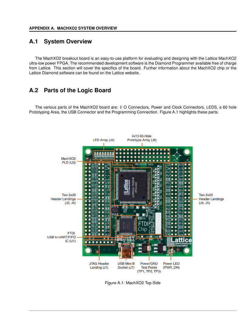
The various parts of the MachXO2 board are: I/ O Connectors, Power and Clock Connectors, LEDS, a 60 holePrototyping Area, the USB Connector and the Programming Connection. Figure A.1 highlights these parts.
Figure A.1: MachXO2 Top Side
A.3. I/O CONNECTORS
A.3 I/O Connectors
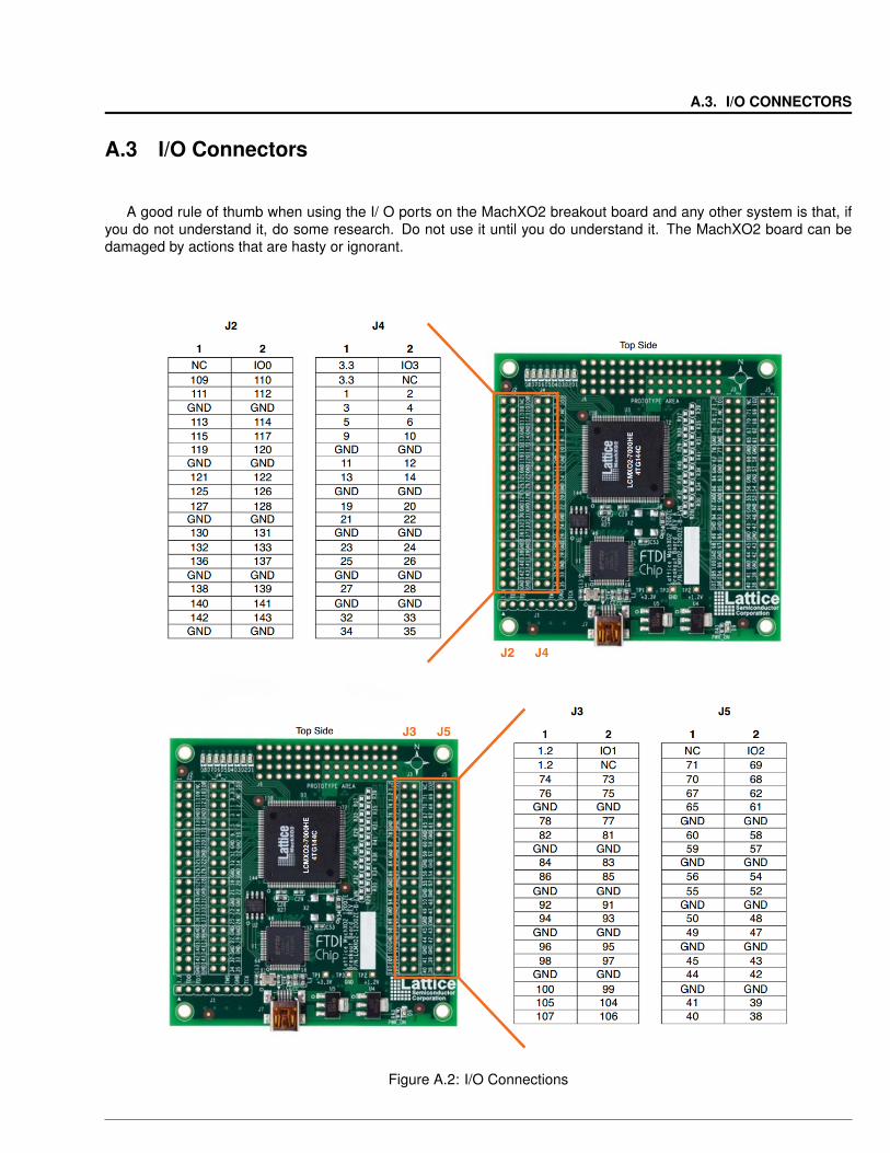
A good rule of thumb when using the I/ O ports on the MachXO2 breakout board and any other system is that, ifyou do not understand it, do some research. Do not use it until you do understand it. The MachXO2 board can bedamaged by actions that are hasty or ignorant.
Figure A.2: I/O Connections
APPENDIX A. MACHXO2 SYSTEM OVERVIEW
A.4 Programming Interface and LED Array
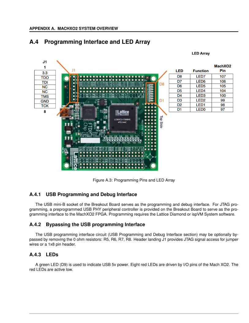
Figure A.3: Programming Pins and LED Array
A.4.1 USB Programming and Debug Interface
The USB mini-B socket of the Breakout Board serves as the programming and debug interface. For JTAG pro-gramming, a preprogrammed USB PHY peripheral controller is provided on the Breakout Board to serve as the pro-gramming interface to the MachXO2 FPGA. Programming requires the Lattice Diamond or ispVM System software.
A.4.2 Bypassing the USB programming Interface
The USB programming interface circuit (USB Programming and Debug Interface section) may be optionally by-passed by removing the 0 ohm resistors: R5, R6, R7, R8. Header landing J1 provides JTAG signal access for jumperwires or a 1x8 pin header.
A.4.3 LEDs
A green LED (D9) is used to indicate USB 5v power. Eight red LEDs are driven by I/O pins of the Mach XO2. Thered LEDs are active low.

A.5. POWER SUPPLY
A.5 Power Supply
When powered from a USB cable, the 3.3V and 1.2V power supply rails are converted from the 5V line on the USBinterface.
A.5.1 Test Points
There are three test points for checking the voltae levels on the MachXO2 board:
TP1: +3.3V
TP2: +1.2V
TP3: GND
A.5.2 Applying External Power
It is possible to power the breakbout board from a source besides the USB input, but it is not recommended. Thebest method is to apply a regulated 5V power source to the USB connector.
Your external power source must be regulated to prevent damage to the MachXO2 board.
A.5.3 Auxiliary Power Output
The 3.3V, 1.2V, and GND pins on the MachXO2 board to provide power to external devices. The on board voltageregulators are capable of supplying a maximum current of 1A. Exceeding the specifications of the regulators cancause them to fail. Read the datasheet for a regulator before attaching higher current devices.

APPENDIX A. MACHXO2 SYSTEM OVERVIEW
Appendix B
Schematics
7
APPENDIX B. SCHEMATICS
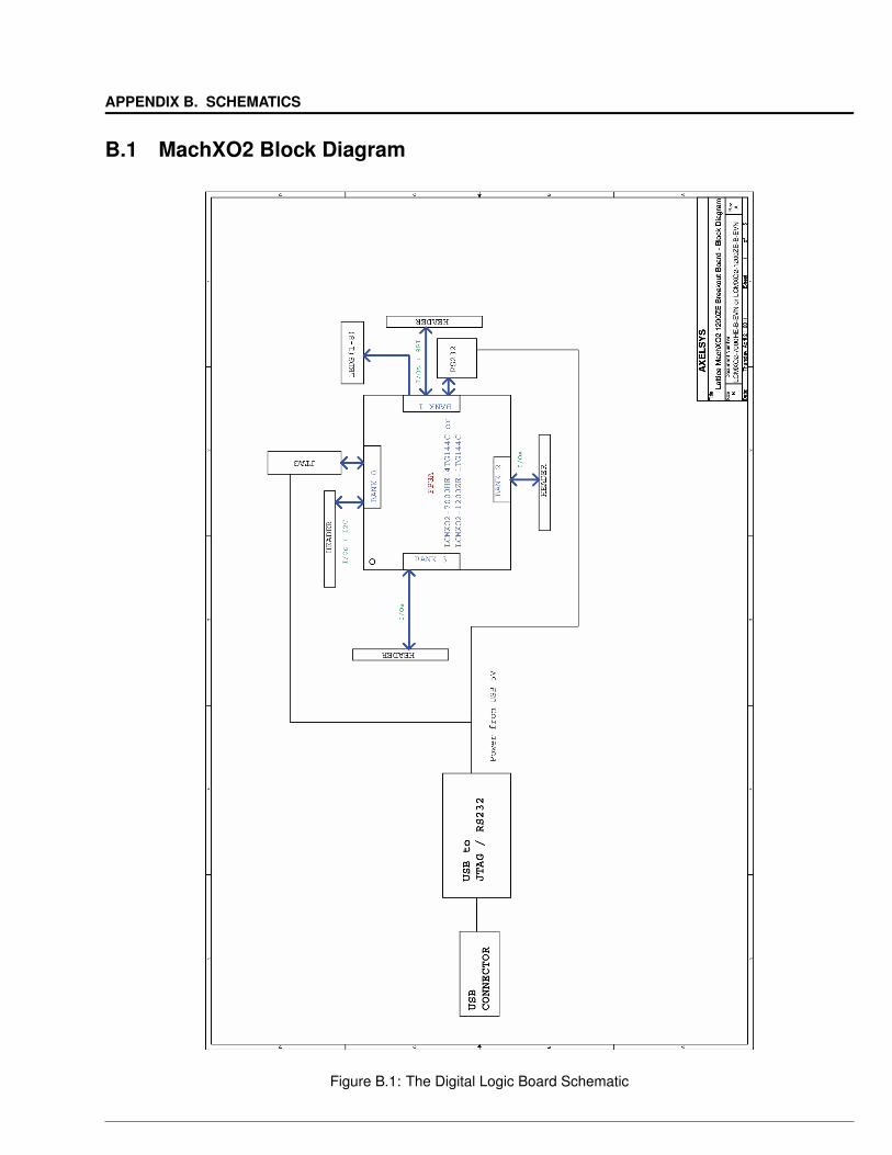
B.1 MachXO2 Block Diagram
Figure B.1: The Digital Logic Board Schematic

B.2. USB INTERFACE TO JTAG
B.2 USB Interface to JTAG
Figure B.2: Power Supplies Schematic

APPENDIX B. SCHEMATICS
B.3 FPGA
Figure B.3: FPGA Schematic
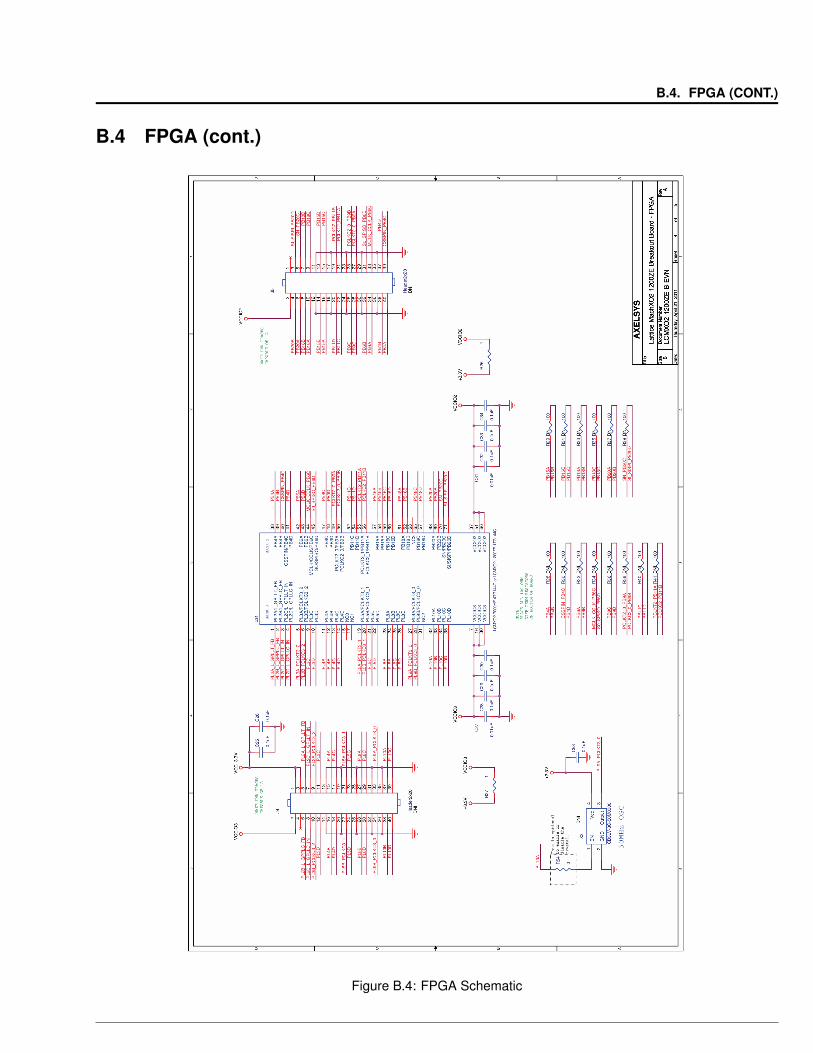
B.4. FPGA (CONT.)
B.4 FPGA (cont.)
Figure B.4: FPGA Schematic
APPENDIX B. SCHEMATICS
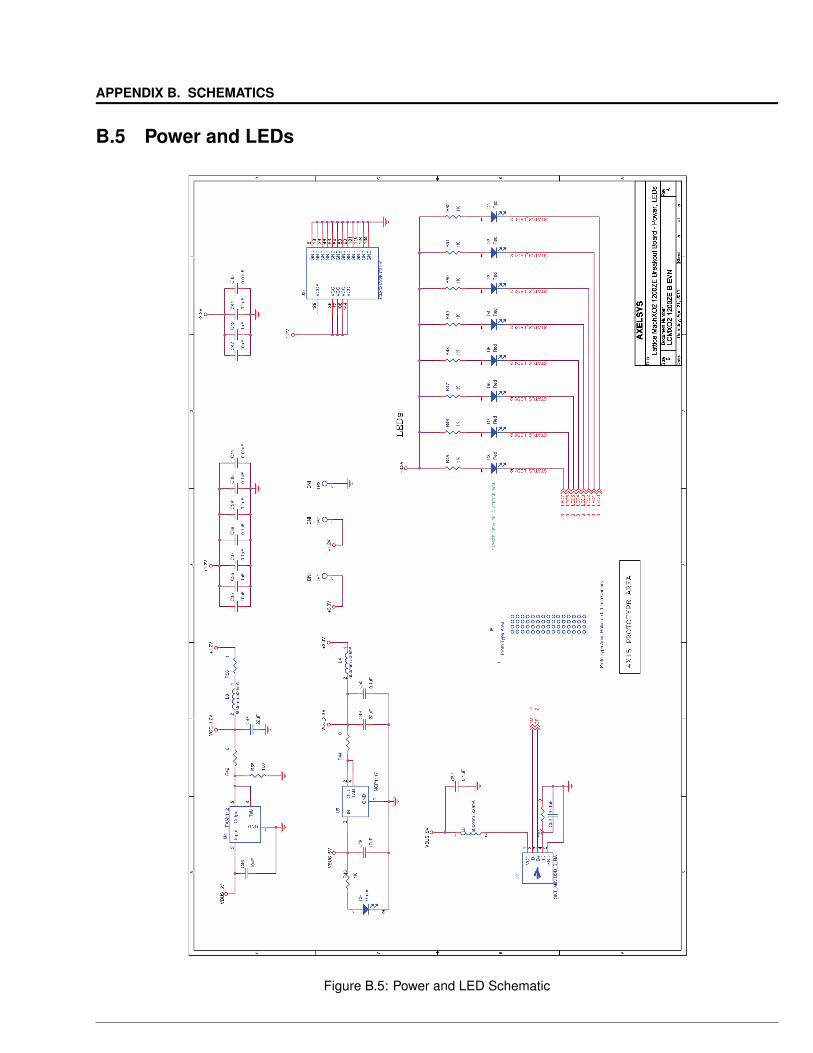
B.5 Power and LEDs
Figure B.5: Power and LED Schematic
B.6. USB BUCK BOOST CONVERTER
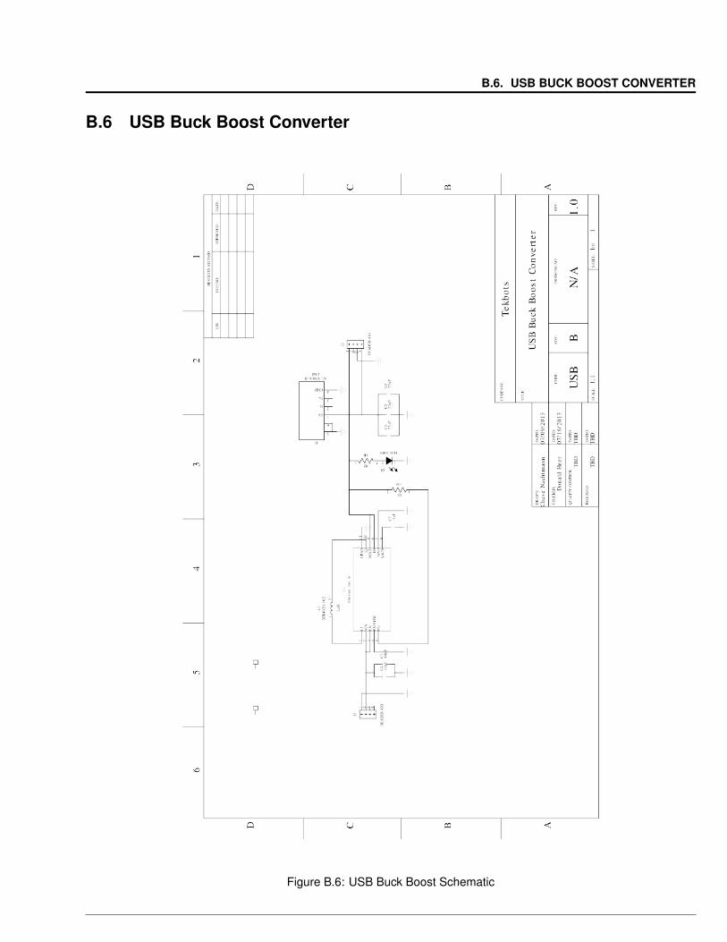
B.6 USB Buck Boost Converter
Figure B.6: USB Buck Boost Schematic
APPENDIX B. SCHEMATICS
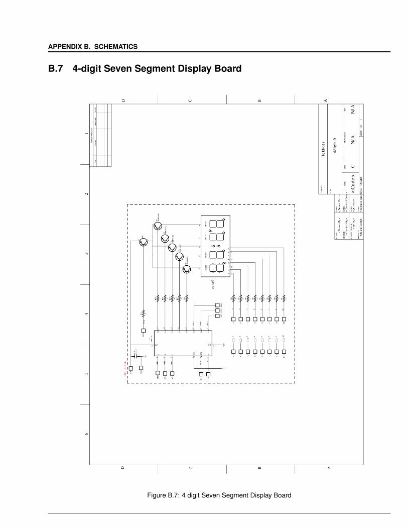
B.7 4-digit Seven Segment Display Board
Figure B.7: 4 digit Seven Segment Display Board
B.8. PUSH BUTTON BOARD
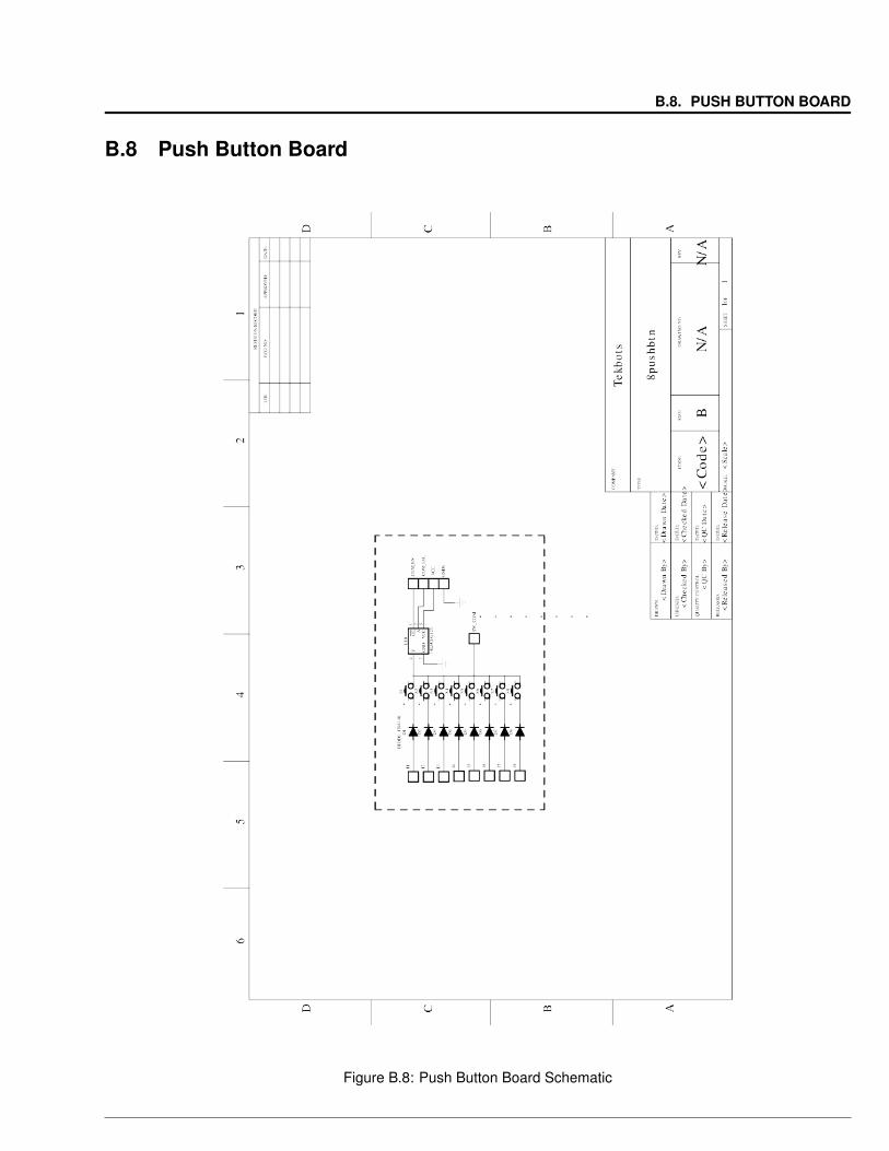
B.8 Push Button Board
Figure B.8: Push Button Board Schematic

APPENDIX B. SCHEMATICS

Appendix C
Silk Screens and Pinouts
17
APPENDIX C. SILK SCREENS AND PINOUTS
This appendix has all the silk screens and pinouts used in this course.
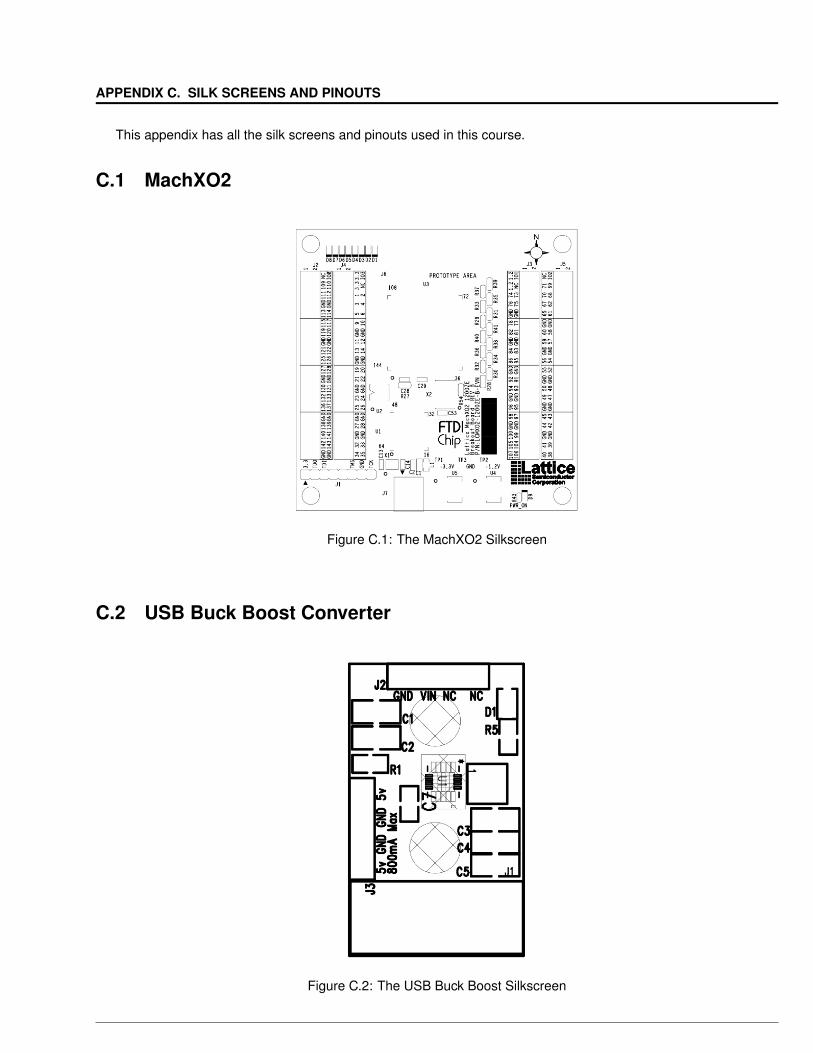
C.1 MachXO2
Figure C.1: The MachXO2 Silkscreen
C.2 USB Buck Boost Converter
Figure C.2: The USB Buck Boost Silkscreen
C.3. 4-DIGIT SEVEN SEGMENT DISPLAY BOARD
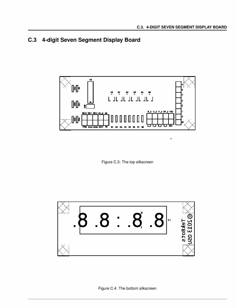
C.3 4-digit Seven Segment Display Board
Figure C.3: The top silkscreen
Figure C.4: The bottom silkscreen
APPENDIX C. SILK SCREENS AND PINOUTS
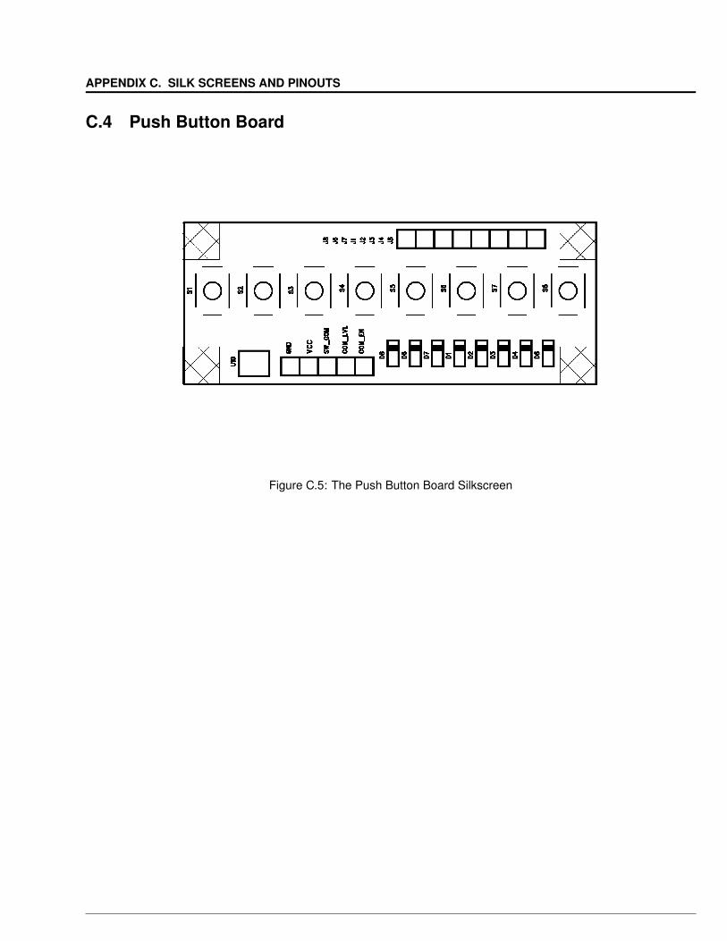
C.4 Push Button Board
Figure C.5: The Push Button Board Silkscreen
Appendix D
Parts and Suppliers
21

APPENDIX D. PARTS AND SUPPLIERS
D.1 Parts List
Board Qty. Description Ref. Fig. Supplier Supplier #MachXO2Breakout
1 MachXO2 Digi-Key 220-1518-ND5 2 x5 Male Header .1” A
USB Buck Boost 1 USB Buck Boost Converter TekBots usb pwr.01 1 x 4 Female Header .1” B Digi-key S7002-ND
4-digit SevenSegment
1 Display Board TekBots 4digit.01 4 digit 7 Segment LED, Yellow, CA L5 C Digi-Key 160-1546-5-ND14 1/8 Watt Resistors R1-R9, R23,
R27-R29E Mouser 299-XXX-RC
Single Row Male Header .1” D Jameco 20768262 2 x 5 Male Header .1” A
Push Button
1 Push Button Board TekBots 8pushbtn.08 1N4148 Diode D11-D17 F Digi-Key 568-1360-1-ND8 Tactile Switch 6x6mm S5-S12 G Mouser 101-06610EV
Single Row Male Header .1” D Jameco 2076826
Figure D.1: Use these figures to determine which parts to use.
D.2 Suppliers List
Digi-Key
701 Brooks Ave. SouthThief River Falls, MN 56701-0677(800) 344-4539http://www.digikey.com
Mouser Electronics
1000 N. Main StreetMansfield, TX 76063(800) 346-6873http://www.mouser.com
TekBots
1110 Kelley Engineering CenterOregon State UniversityCorvallis, OR 97331http://eecs.oregonstate.edu/tekbots
Jameco Electronics
1355 Shoreway RdBelmont, CA 94002(800) 831-4242http://www.jameco.com


