30
MACOM GaN Reliability Presentation GaN on Silicon Processes and Products 1
MACOM GaN Reliability Presentation GaN on Silicon Processes and Products
1

MACOM GaN on Silicon Reliability Presentation

MACOM GaN Strategy
GaN on Silicon Carbide •0.5um GaN HEMT process •0.25um GaN HEMT process •Dual wafer foundries •Reliable plastic packaging
GaN on Silicon •Silicon cost structure •0.5um GaN HEMT process •0.25um GaN HEMT in 2014 •Reliable plastic packaging •Epitaxial 8” agreement
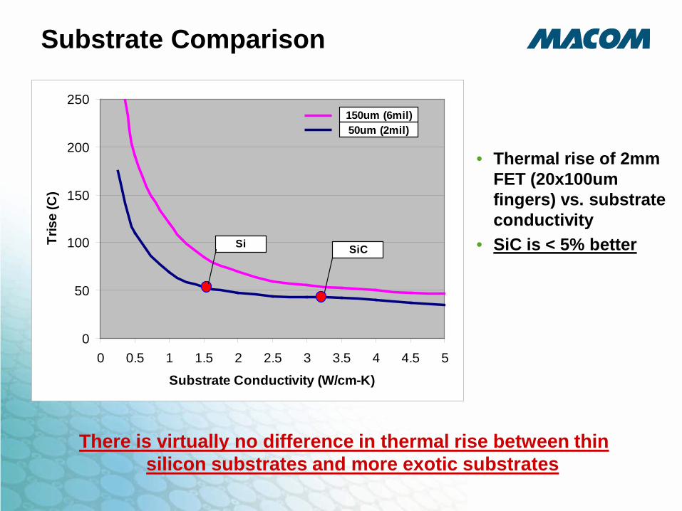
Substrate Comparison
• Thermal rise of 2mm FET (20x100um fingers) vs. substrate conductivity
• SiC is < 5% better
There is virtually no difference in thermal rise between thin silicon substrates and more exotic substrates
0
50
100
150
200
250
0 0.5 1 1.5 2 2.5 3 3.5 4 4.5 5
Substrate Conductivity (W/cm-K)
Tris
e (C
)
Si SiC
150um (6mil)50um (2mil)

Ex: Thermal Analysis of 100W GaN Devices
GaN – 2um
Si – 50um
Au/Sn – 4um
Cu Package – 1.5mm
0.02°C/W
0.52°C/W
0.22°C/W
0.62°C/W
150μm to 50μm die thickness CuW to pure Cu package
GaN – 2um
Si – 150um
Au/Si – 4um
CuW Package – 1.5mm
0.02°C/W
0.77°C/W
0.22°C/W
0.8°C/W
NPT25100, Gen 1 RTH = 1.8°C/W
NPT1010, Gen 2 RTH = 1.4°C/W
= 25% Improvement = 24% Improvement
Many contributors to total thermal impedance Substrate contribution is only about 1/3 of total

Measure RTH on Every Product Design
DC Thermal Imaging: VDS = 28V, ID = 600mA PDISS = 16.8W
NPT25100 NPT1010
RJC = 1.8 oC/W RJC ~ 1.4 oC/W
Process Qualification
Process Qualification Philosophy
• Determine Dominant EOL Failure Mechanism – Diffusion based failure mechanism
• Wearout mechanism • Characterized by change in IDS
– Temperature accelerated life test • 3 temperature ALT • Step stress determined ALT junction temperatures • Design test for reasonable mean time to failure at each
temperature – Perform
• New or changed design process, e.g. transistor structure • New or changed fabrication process
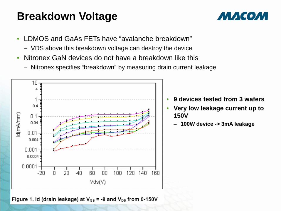
Breakdown Voltage
• LDMOS and GaAs FETs have “avalanche breakdown” – VDS above this breakdown voltage can destroy the device
• Nitronex GaN devices do not have a breakdown like this – Nitronex specifies “breakdown” by measuring drain current leakage
• 9 devices tested from 3 wafers • Very low leakage current up to
150V – 100W device -> 3mA leakage
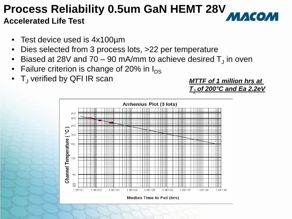
Process Reliability 0.5um GaN HEMT 28V Accelerated Life Test
• Test device used is 4x100µm • Dies selected from 3 process lots, >22 per temperature • Biased at 28V and 70 – 90 mA/mm to achieve desired TJ in oven • Failure criterion is change of 20% in IDS • TJ verified by QFI IR scan MTTF of 1 million hrs at
TJ of 200°C and Ea 2.2eV

Enhanced Breakdown Voltage
Achieved >200V breakdown voltage for 48V NRF2 Technology
-3
-2
-1
0
1
2
Lo
g ID
LK
0 20 40 60 80 100 120 140 160 180 200Vd
-3
-2
-1
0
1
2
Lo
g IG
LK
Plot for Geom=GD2
-3
-2
-1
0
1
2
Lo
g ID
LK
0 20 40 60 80 100 120 140 160 180 200Vd
-3
-2
-1
0
1
2
Lo
g IG
LK
Plot for Geom=GD3
-3
-2
-1
0
1
2
Lo
g ID
LK
0 20 40 60 80 100 120 140 160 180 200Vd
-3
-2
-1
0
1
2
Lo
g IG
LK
Plot for Geom=GD4
GD2
Left Scale: Log IDLKRight Scale: Log IGLK
Gate-Drain Spacing 2 microns Gate-Drain Spacing 3 microns Gate-Drain Spacing 4 microns
GD3 28V Technology
GD4 48V Technology
• BV Testing shows expected trend of increasing BV with GD spacing (~50-80V/µm).
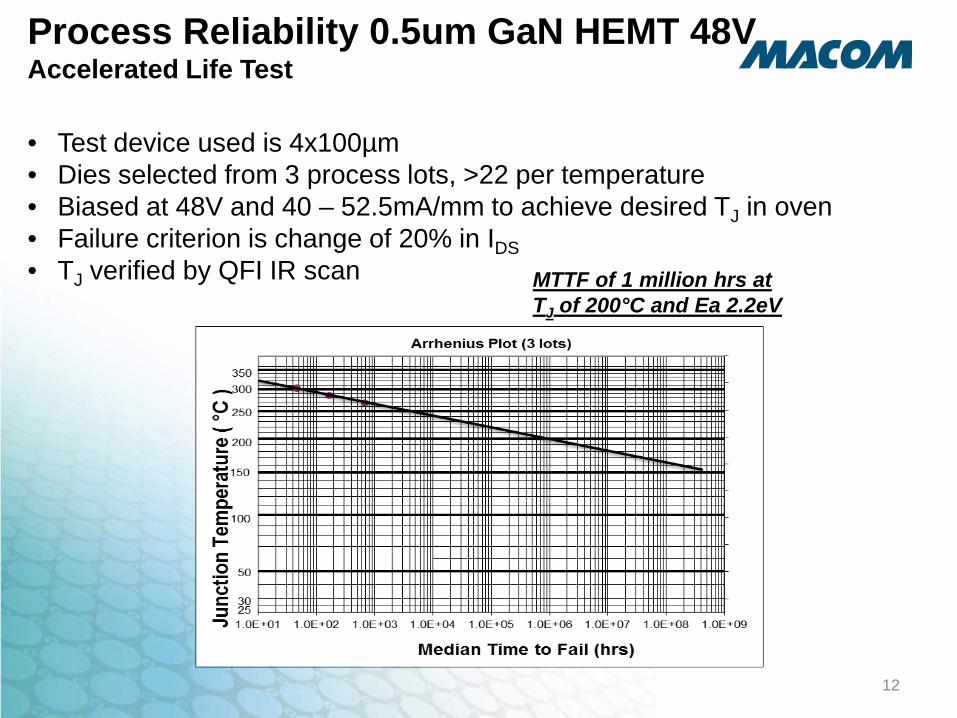
Process Reliability 0.5um GaN HEMT 48V Accelerated Life Test
12
• Test device used is 4x100µm • Dies selected from 3 process lots, >22 per temperature • Biased at 48V and 40 – 52.5mA/mm to achieve desired TJ in oven • Failure criterion is change of 20% in IDS • TJ verified by QFI IR scan MTTF of 1 million hrs at
TJ of 200°C and Ea 2.2eV

Product Qualification
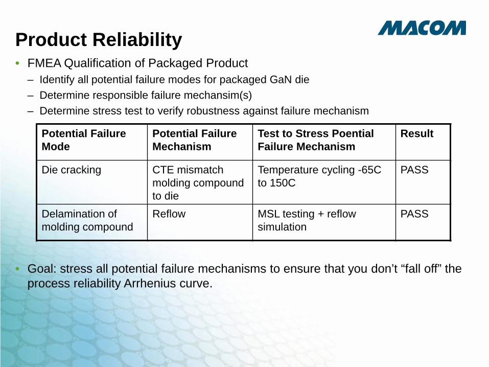
Product Reliability • FMEA Qualification of Packaged Product
– Identify all potential failure modes for packaged GaN die – Determine responsible failure mechansim(s) – Determine stress test to verify robustness against failure mechanism
• Goal: stress all potential failure mechanisms to ensure that you don’t “fall off” the process reliability Arrhenius curve.
Potential Failure Mode
Potential Failure Mechanism
Test to Stress Poential Failure Mechanism
Result
Die cracking CTE mismatch molding compound to die
Temperature cycling -65C to 150C
PASS
Delamination of molding compound
Reflow MSL testing + reflow simulation
PASS
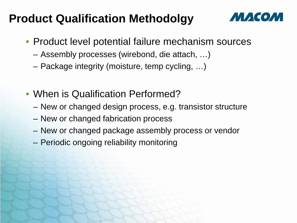
Product Qualification Methodolgy
• Product level potential failure mechanism sources – Assembly processes (wirebond, die attach, …) – Package integrity (moisture, temp cycling, …)
• When is Qualification Performed?
– New or changed design process, e.g. transistor structure – New or changed fabrication process – New or changed package assembly process or vendor – Periodic ongoing reliability monitoring
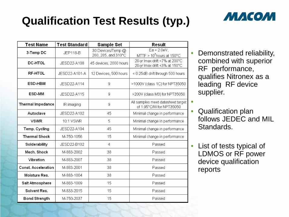
Qualification Test Results (typ.)
• Demonstrated reliability, combined with superior RF performance, qualifies Nitronex as a leading RF device supplier.
• • Qualification plan
follows JEDEC and MIL Standards.
• List of tests typical of LDMOS or RF power device qualification reports
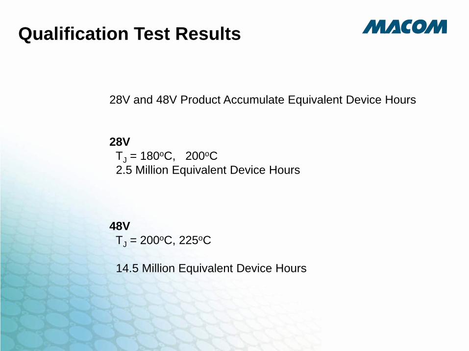
28V and 48V Product Accumulate Equivalent Device Hours 28V TJ = 180oC, 200oC 2.5 Million Equivalent Device Hours 48V TJ = 200oC, 225oC 14.5 Million Equivalent Device Hours
Qualification Test Results

NPT2022 Thermal Resistance Method
18
• RJC = 1.3 C/W (48V) @ 225 TJ • Important to determine Rth at high temp
• Rth determined using 3um
• Same IR method used for accelerated life test junction temperature determination
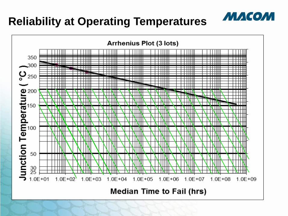
Reliability at Operating Temperatures

Plastic Package HTOL (<25W)
• Constant IDS system, software controlled • Constant in-situ monitoring of VDS, VGS, IGS,
IDS
• T0 (initial) tests and periodic down point testing performed in-situ
• Testing includes both DC and RF msmts
20
System Description • 4 systems, 32 DUTs
per system • Hot plate with chiller
temperature controlled to +/1°C
HTOL Rack Hotplate with burn-in board
RF Test Rack
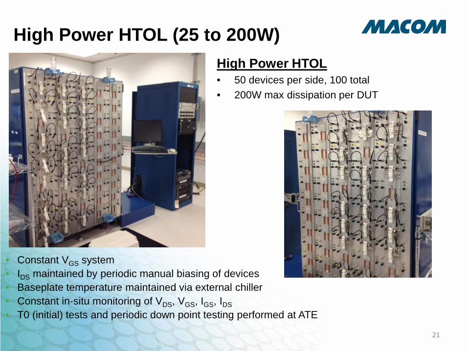
High Power HTOL (25 to 200W)
• Constant VGS system • IDS maintained by periodic manual biasing of devices • Baseplate temperature maintained via external chiller • Constant in-situ monitoring of VDS, VGS, IGS, IDS • T0 (initial) tests and periodic down point testing performed at ATE
21
High Power HTOL • 50 devices per side, 100 total • 200W max dissipation per DUT
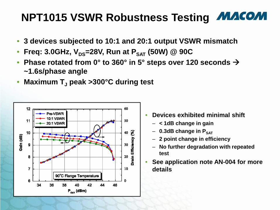
NPT1015 VSWR Robustness Testing
• 3 devices subjected to 10:1 and 20:1 output VSWR mismatch • Freq: 3.0GHz, VDS=28V, Run at PSAT (50W) @ 90C • Phase rotated from 0° to 360° in 5° steps over 120 seconds
~1.6s/phase angle • Maximum TJ peak >300°C during test
• Devices exhibited minimal shift – < 1dB change in gain – 0.3dB change in PSAT
– 2 point change in efficiency – No further degradation with repeated
test • See application note AN-004 for more
details
GaN on Silicon Field Reliability
• 1 million devices fielded – MIL radios and EW – CATV – Infrastructure
• High volume software defined military radio program – 6 years of volume production – Harsh environmental conditions – No field returns to date

GaN Reliability in Your Product

Recommendations for GaN Devices • Use Well Designed Bias Circuits
– Sequence RF, Gate, and Drain Voltages • See application notes
– Avoid glitches, stray RF, that could cause VGS to fail • Charge pump inverters and op-amps are EMI susceptible
– Monitor gate current • High IG indicates severe overdrive
– Bias/decoupling components • Affect risetime, falltime, IM performance, memory effects • Review transient, modulation BW, RF frequency effects • Wideband amplifiers present special challenges
– Gate/drain bias chokes subject to resonances – Look for narrowband loss of efficiency and power – Add resistors, networks to lower or control Q

Stability Considerations
RF In
RF Out
NPTx
VGATE
50 Ω
This value is important
Low Freq Impedance into VGATE must be low
NPTx
50 Ω • Low Frequency Equivalent Circuit
– Gate sees 50 ohms to ground – Verify stability w/ CAD tools – Sweep both model and circuit
• Low Frequency Stability – RF transistors have enormous LF gain – Open (high Z) input = DANGER – Gate resistor tames LF loop gain – Large caps at VGATE and VDRAIN
• Improves stability • Critical for linearity, intermod, ACPR
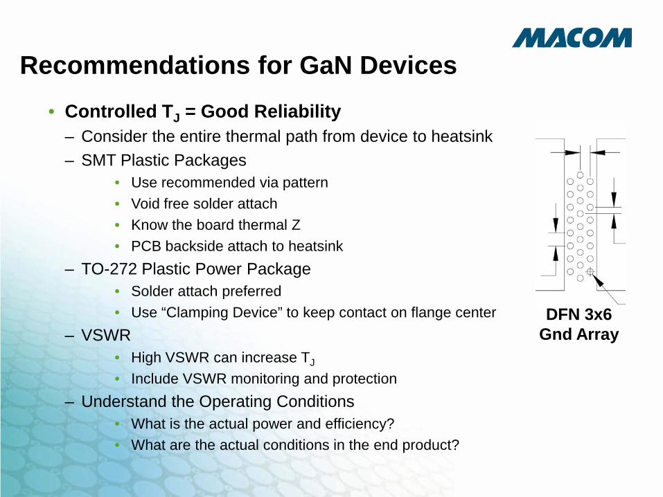
Recommendations for GaN Devices • Controlled TJ = Good Reliability
– Consider the entire thermal path from device to heatsink – SMT Plastic Packages
• Use recommended via pattern • Void free solder attach • Know the board thermal Z • PCB backside attach to heatsink
– TO-272 Plastic Power Package • Solder attach preferred • Use “Clamping Device” to keep contact on flange center
– VSWR • High VSWR can increase TJ
• Include VSWR monitoring and protection – Understand the Operating Conditions
• What is the actual power and efficiency? • What are the actual conditions in the end product?
DFN 3x6 Gnd Array
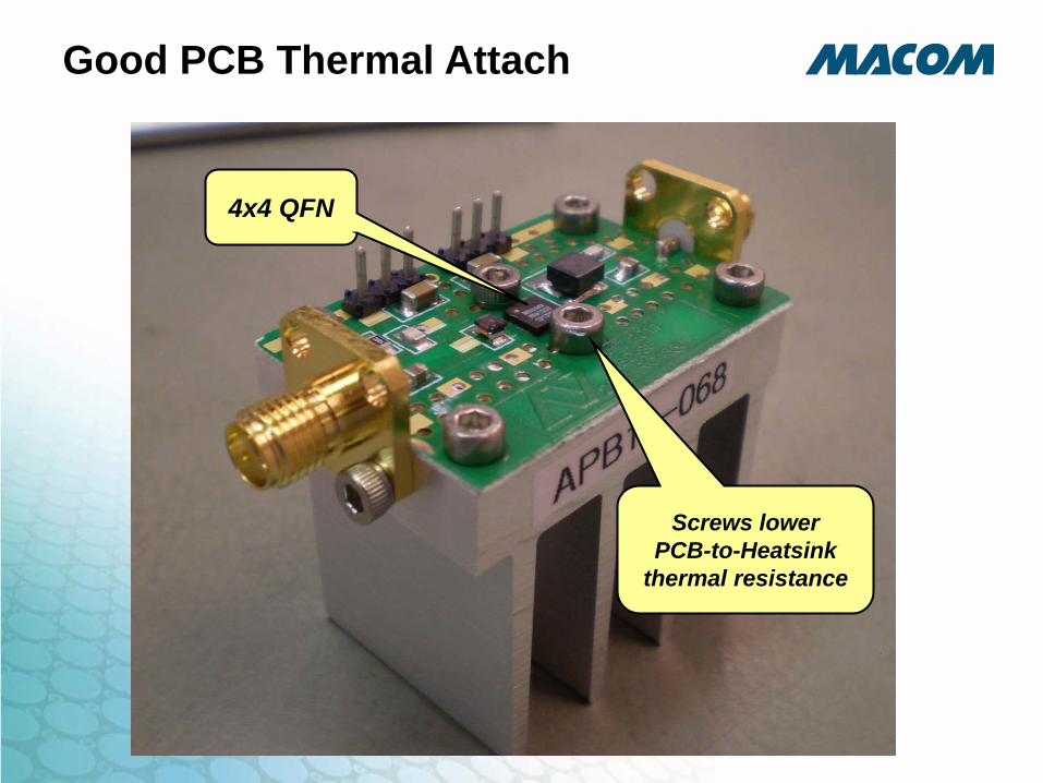
Screws lower PCB-to-Heatsink
thermal resistance
Good PCB Thermal Attach
4x4 QFN

NPTB00025 VSWR Phase Sweep, T ~ 25C NPTB00025 (Dev 14) in Tj vs Phase Angle for 15:1 VSWR Testing
(To=25C & RTH=5.25C/W) at 3GHz
0
50
100
150
200
250
300
350
0 45 90 135 180 225 270 315 360
Phase Angle (degrees)
Tj (C
) an
d Pd
iss(
W)
-5
0
5
10
15
20
25
30
35
40
45
50
55
60
65
Gat
e C
urre
nt (m
A)
15:1 VSWR Stress Test
Pdiss-15:1 VSWR
Ig (mA)
• A high junction temperature is reached (250°C) is reached • A high gate current is observed out-of-phase to maximum temperature • A rugged device withstands high voltages at ~100°C channel temperature

Thermal Budgeting
• Typical Thermal Budget – NPT2022 48V@100W RTH = 1.3°C/W – “100W” is “rated power” in a narrowband test circuit
• Most vendors use the same ratings
– Broadband power will be lower • Depends on bandwidth and matching circuit • How close to ZOPT?
– Ex: 100-1000 MHz Broadband Amplifier • Delivers 80W @ 50% worst case efficiency • PDISS = 80W (DC) + 5W (PIN) • TRISE = 85W * 1.3°C/W = 111°C • Max TFLANGE = 89C for TJ = 200°C
This design has good thermal margin


