A Science & Technology Center Magnetization Switching Using Spin Orbit Torques from Sputtered Conductive WTe x Xiang (Shaun) Li, Mahendra DC, Chong Bi, and S. X. Wang Materials Science and Engineering, Electrical Engineering Peng Li, Yuri Suzuki Applied Physics Stanford University 2019 E3S Annual Retreat University of California, Berkeley, September 19-20, 2019
Transcript
A Science & Technology Center
Magnetization Switching Using Spin Orbit Torques from Sputtered Conductive WTex
Xiang (Shaun) Li,
Mahendra DC, Chong Bi, and S. X. WangMaterials Science and Engineering, Electrical Engineering
Peng Li, Yuri SuzukiApplied Physics
Stanford University
2019 E3S Annual RetreatUniversity of California, Berkeley, September 19-20, 2019
A Science & Technology Center
9/19/2019 Page 2
0.1
1
10
100
1000
10000
Read time (ns)
Write time (ns)
Cell size (F2)Read energy (fJ)
Write energy (fJ)
SRAMeDRAMDRAMSTT-MRAMFeFETReRAMPCM
Xiang Li, Kang L. Wang, et al., MRS Bulletin, vol. 43, pp. 970-977, 2018.
S. Salahuddin, K. Ni, and S. Datta, Nature Electronics, vol. 1, pp. 442-450, 2018.
Standby Power
Limited Endurance
Comparison of Existing and Emerging Memories
A Science & Technology Center
SOT-MRAM Towards SRAM Performance
Page 39/19/2019
Bit switching energy estimates:
~250 fJ @ 110 nm
Scaling down possibility:
~10 fJ @ 22 nm ~0.5 fJ @ 5 nm
Sato, Wang, et al., Nature Electronics, 1(9), 508, 2018
C. O. Avci et al., Nature Physics, vol. 11, p. 570, 2015.
Xiang Li, Shan Wang, et al., in preparation
A Science & Technology Center
Current-Induced Field-Free Switching
Page 119/19/2019
• Switching current density in WTex 0.77-1.41 MA/cm2
-15 -10 -5 0 5 10 15
-10
-5
0
5
-5000 0 5000-4
-2
I = 0.7 mA
R x
x
2
(m
)
Hy (Oe)
-8 -4 0 4 8
-10
-5
0
5
Ipulse
(mA)
R x
x
2
(m
)
- My initialization
My initialization
H = 0
tpulse
= 1 ms
Xiang Li, Shan Wang, et al., in preparation
A Science & Technology Center
Resistivity (𝜇Ω ⋅ 𝑐𝑚)
𝜉 𝑆𝑇
0.1
1
10
100
100 1000 10000
Benchmark: Power Efficiency of SOT-MTJ Cell
Page 129/19/2019
Physical Review Applied, vol. 10, Sep 6 2018.
Assumes 6 nm SOT write line under 1 nm in-plane CoFeB.
Resistivity (𝜇Ω 𝑐𝑚)
Pow
er
1
10
100
100 1000 10000
435.2
300
713
12000
Sputtered WTex
Sputtered WExfoliated WTe2*Sputtered BiSex**
Xiang Li, Shan Wang, et al., in preparation
*Yang et al., Nature
Nano, 2019.
**Wang et al.,
Nature Materials,
2018.
A Science & Technology Center
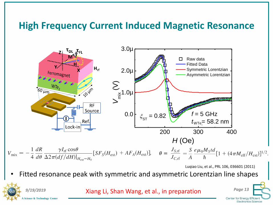
High Frequency Current Induced Magnetic Resonance
2018 NSF Site Visit Page 139/19/2019
• Fitted resonance peak with symmetric and asymmetric Lorentzian line shapes
𝜃 =
Luqiao Liu, et al., PRL 106, 036601 (2011)
Raw data
Fitted Data
Symmetric Lorentzian
Asymmetric Lorentzian
200 300 400
0.0
1.0µ
2.0µ
3.0µ
WTeX
Vm
ix (
V)
H (Oe)
f = 5 GHz
t = 58.2 nm
ST = 0.82
Xiang Li, Shan Wang, et al., in preparation
A Science & Technology Center
SOT-MTJ Integration and Test
Page 149/19/2019
A Science & Technology Center
Conclusions
• MRAM holds great promise to replace or complement SRAM for data-centric applications as high-density on-chip memory
• Unique topological band structure gives rise to highly spin polarized electrons in Weyl semimetal WTe2
• Sputtered 5 nm WTex at room temperature shows attractive charge-to-spin conversion efficiency (0.5), low switching current density (1 MA/cm2), and low thin film resistivity (570 𝝁𝛀⋅𝒄𝒎)
• Greatly improved energy/delay performance compared with other topological materials such as BiSe or exfoliated WTe2
• Even larger charge-to-spin conversion efficiency up to 0.8