S. Coffa, Si Optoelectronics, Bioelectonics and Nano-Organics, Corporate R&D, ESSDERC 2002, Florence, September 22th, 2002 Materials, devices and applications Materials, devices and applications of of Si Si - - based based optoelectronics optoelectronics S. Coffa Si Optoelectronics, bioelectronics and nano-organics Corporate R&D, STMicroelectronics, Catania
Transcript
S. Coffa, Si Optoelectronics, Bioelectonics and Nano-Organics, Corporate R&D, ESSDERC 2002, Florence, September 22th, 2002
Materials, devices and applications Materials, devices and applications of of SiSi--based based optoelectronicsoptoelectronics
S. Coffa
Si Optoelectronics, bioelectronics and nano-organicsCorporate R&D, STMicroelectronics, Catania
S. Coffa, Si Optoelectronics, Bioelectonics and Nano-Organics, Corporate R&D, ESSDERC 2002, Florence, September 22th, 2002
OutlineOutlineAims
Scientific challenges, targets and market perspectives ofSi-based optoelectronics
ApplicationsFabrication, performances and applications of Si-based optical devicesIntegrated Si-based optoelectronics as enabling technology in multifunctional devices
• Biosensors• Novel optical memories and molecular switches
Conclusions
STMicroelectronics
Scientific challenges, targets and market perspectives of Si-based optoelectonics
S. Coffa, Si Optoelectronics, Bioelectonics and Nano-Organics, Corporate R&D, ESSDERC 2002, Florence, September 22th, 2002
Science and Technology for Fun and Profit
S. Coffa, Si Optoelectronics, Bioelectonics and Nano-Organics, Corporate R&D, ESSDERC 2002, Florence, September 22th, 2002
OPTICAL SMCOPTICAL SMCvs TOTAL SMC DEVICESTOTAL SMC DEVICESWW REVENUE and FORECAST 99-05
($M)
Optical Semicond. Devices MS
4.1% in 99 5.6% in 05
S. Coffa, Si Optoelectronics, Bioelectonics and Nano-Organics, Corporate R&D, ESSDERC 2002, Florence, September 22th, 2002
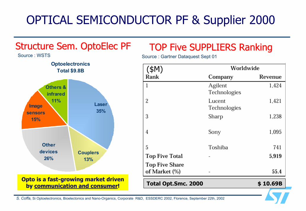
OPTICAL SEMICONDUCTOR PF & Supplier 2000
OptoelectronicsTotal $9.8B
Laser35%
Couplers13%
Other devices
26%
Image sensors
15%
Others & infrared
11%
Source : WSTSStructure Sem. OptoElec PF Structure Sem. OptoElec PF TOP Five SUPPLIERS Ranking
($M)
TOP Five SUPPLIERS Ranking Source : Gartner Dataquest Sept 01
Opto is a fast-growing market driven by communication and consumer! Total Opt.Smc. 2000 $ 10.69B
S. Coffa, Si Optoelectronics, Bioelectonics and Nano-Organics, Corporate R&D, ESSDERC 2002, Florence, September 22th, 2002
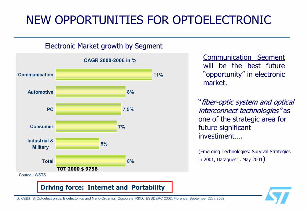
NEW OPPORTUNITIES FOR OPTOELECTRONIC
Electronic Market growth by SegmentElectronic Market growth by Segment
Communication Segmentwill be the best future “opportunity” in electronic market.
CAGR 2000-2006 in %
11%
8%
7%
5%
8%
7,5%
Communication
Automotive
PC
Consumer
Industrial &Military
TotalTOT 2000 $ 975B
“fiberfiber--optic system and optical optic system and optical interconnect technologies”interconnect technologies” as one of the strategic area for future significant investiment….
(Emerging Technologies: Survival Strategies
in 2001, Dataquest , May 2001)
Source : WSTSSource : WSTS
Driving force: Internet and Portability
S. Coffa, Si Optoelectronics, Bioelectonics and Nano-Organics, Corporate R&D, ESSDERC 2002, Florence, September 22th, 2002
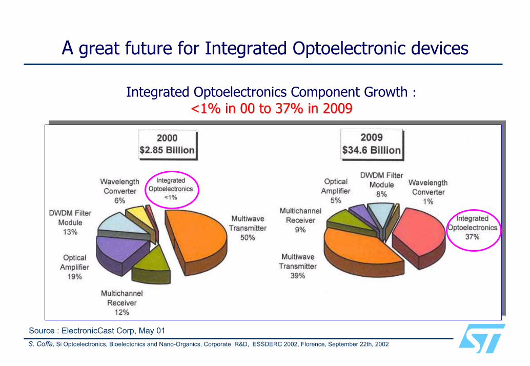
A great future for Integrated Optoelectronic devices
Integrated Optoelectronics Component Growth :<1% in 00<1% in 00 to 37% in 2009to 37% in 2009
Source : ElectronicCast Corp, May 01
S. Coffa, Si Optoelectronics, Bioelectonics and Nano-Organics, Corporate R&D, ESSDERC 2002, Florence, September 22th, 2002
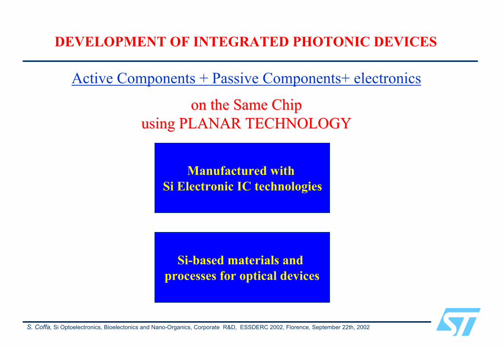
DEVELOPMENT OF INTEGRATED PHOTONIC DEVICES
Active Components + Passive Components+ electronics
on the Same Chipon the Same Chipusing PLANAR TECHNOLOGYusing PLANAR TECHNOLOGY
Manufactured with Si Electronic IC technologies
Si-based materials and processes for optical devices
STMicroelectronics
Fabrication, performances and applications of Si-based optical devices
See also: D21.3 Quantum dot materials and devices for light emission in Si by M.E. Castagna et al. DP.28 Integrated Si-based Opto-couplers: a novel approach to galvanic insulation by A. Alessandria et. al
S. Coffa, Si Optoelectronics, Bioelectonics and Nano-Organics, Corporate R&D, ESSDERC 2002, Florence, September 22th, 2002
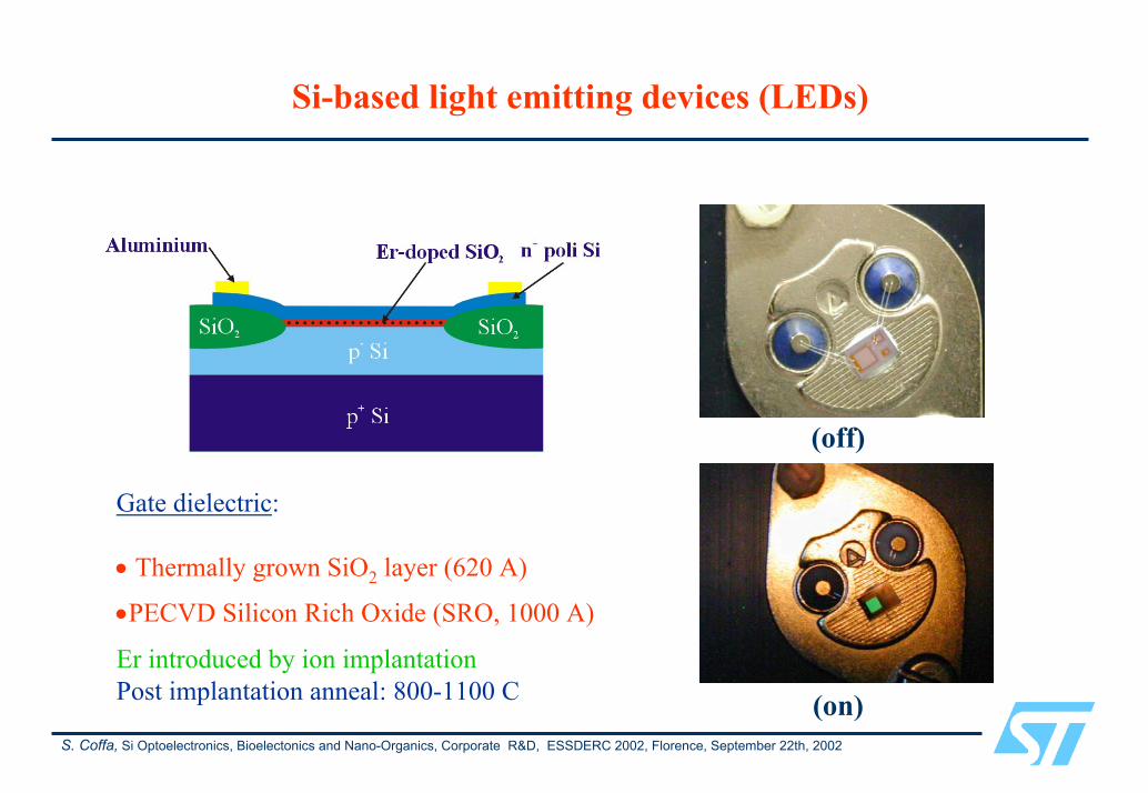
Si-based light emitting devices (LEDs)
(off)
Gate dielectric:
• Thermally grown SiO2 layer (620 A)
•PECVD Silicon Rich Oxide (SRO, 1000 A)
Er introduced by ion implantationPost implantation anneal: 800-1100 C (on)
S. Coffa, Si Optoelectronics, Bioelectonics and Nano-Organics, Corporate R&D, ESSDERC 2002, Florence, September 22th, 2002
World record efficiency for Si-based LEDs
• We have fabricated the world-record Si-based LED using Si processing •The efficiency (10%) is similar to that of state-of-the art
LED using III-V semiconductors
S. Coffa, Si Optoelectronics, Bioelectonics and Nano-Organics, Corporate R&D, ESSDERC 2002, Florence, September 22th, 2002
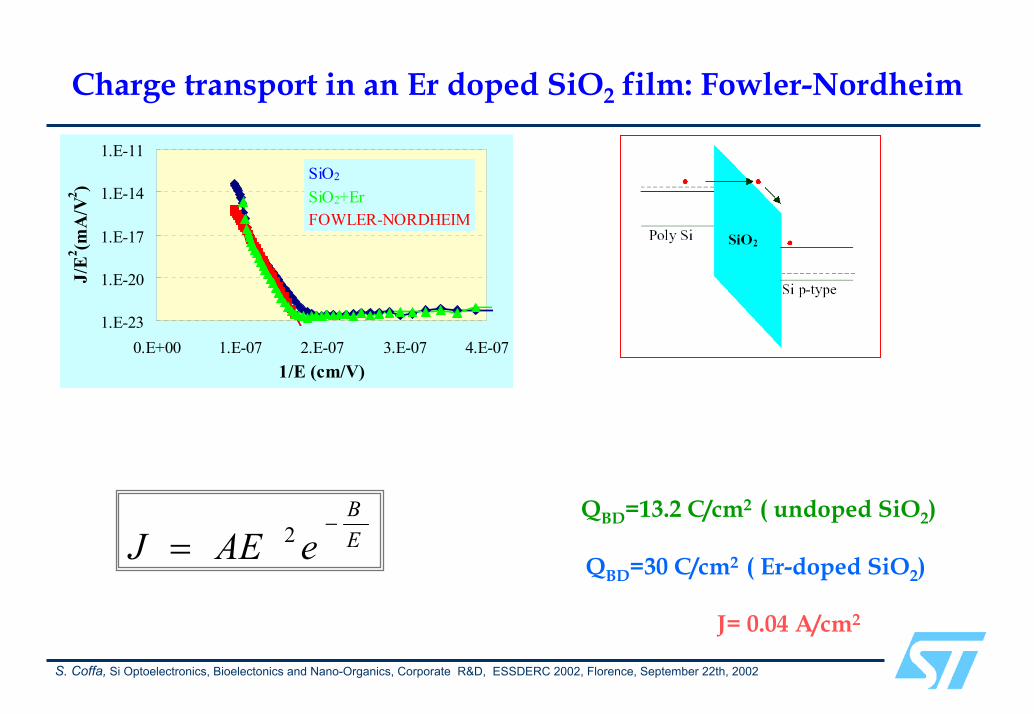
Charge transport in an Er doped SiO2 film: Fowler-Nordheim
1.E-23
1.E-20
1.E-17
1.E-14
1.E-11
0.E+00 1.E-07 2.E-07 3.E-07 4.E-071/E (cm/V)
J/E
2 (mA
/V2 )
SiO2
SiO2+ErFOWLER-NORDHEIM
EB
eAEJ−
= 2QBD=13.2 C/cm2 ( undoped SiO2)
QBD=30 C/cm2 ( Er-doped SiO2)
J= 0.04 A/cm2
S. Coffa, Si Optoelectronics, Bioelectonics and Nano-Organics, Corporate R&D, ESSDERC 2002, Florence, September 22th, 2002
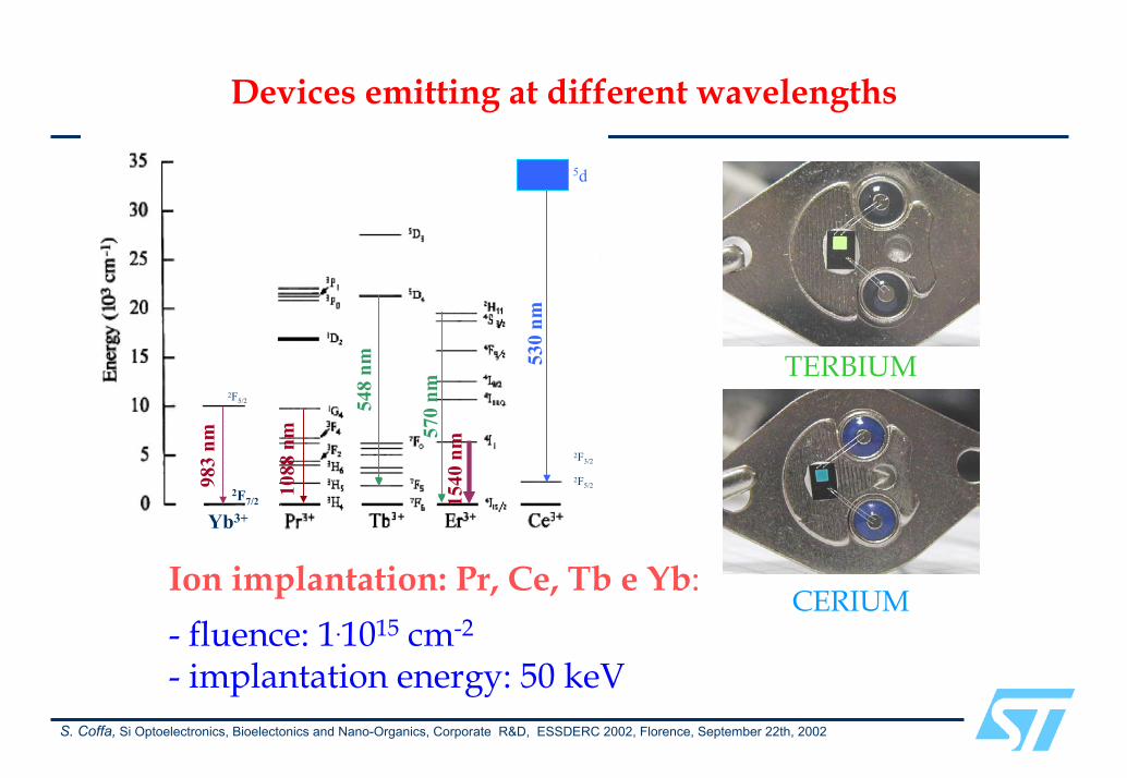
Devices emitting at different wavelengths
2F5/2
2F3/2
1088
nm
548
nm
1540
nm57
0 nm
5d
530
nm
2F7/2
2F5/2
983
nm
Yb3+
Ion implantation: Pr, Ce, Tb e Yb:- fluence: 1.1015 cm-2
- implantation energy: 50 keV
TERBIUM
CERIUM
S. Coffa, Si Optoelectronics, Bioelectonics and Nano-Organics, Corporate R&D, ESSDERC 2002, Florence, September 22th, 2002
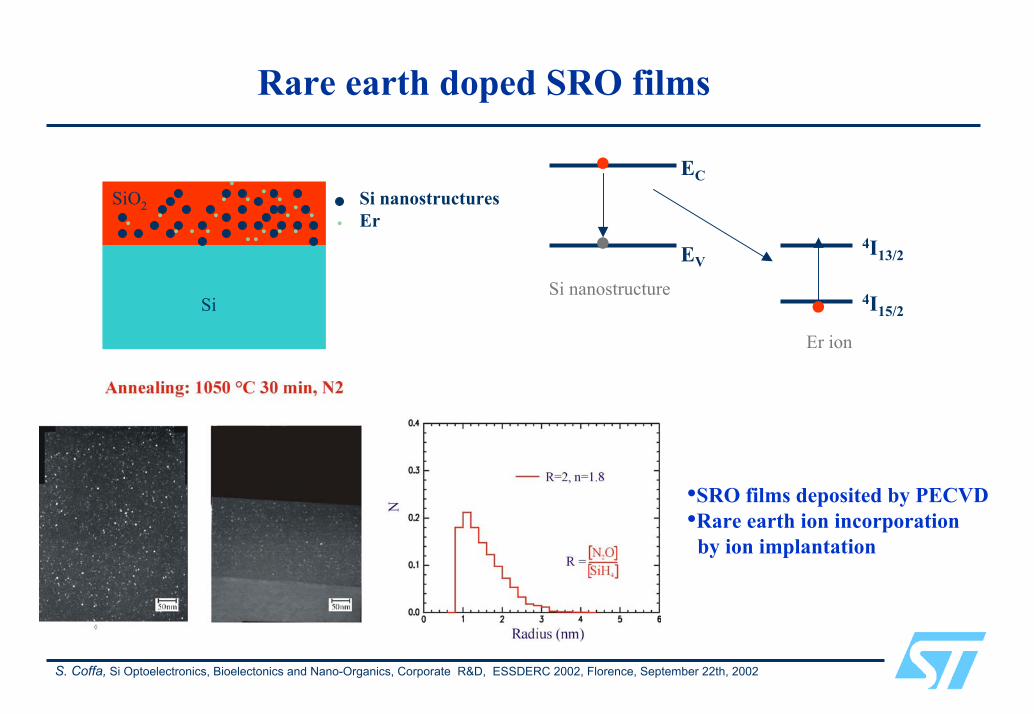
Rare earth doped SRO films
EC
Si
SiO2 Si nanostructuresEr
EV4I13/2
Si nanostructure 4I15/2
Er ion
•SRO films deposited by PECVD•Rare earth ion incorporation
by ion implantation
S. Coffa, Si Optoelectronics, Bioelectonics and Nano-Organics, Corporate R&D, ESSDERC 2002, Florence, September 22th, 2002
ElectroElectro--luminescence from Erluminescence from Er--doped SRO filmsdoped SRO films
Annealing temperature: 800oC
0
1000
2000
3000
4000
5000
1470 1520 1570WAVELENGTH (nm)
EL
Inte
nsity
( µV
)
SRO (n=1.70) + ErSRO (n=1.64) + ErSRO (n=1.61) + Er SRO: best
•Motor control•Power supplies•Solid state relays•Power meters
CIRCUITB
CIRCUIT A POWER
DEVICEOPTO
INSULATOR
S. Coffa, Si Optoelectronics, Bioelectonics and Nano-Organics, Corporate R&D, ESSDERC 2002, Florence, September 22th, 2002
Galvanic insulation using Galvanic insulation using SiSi--based based optoelectonicsoptoelectonics
•Low cost SOI•Er-doped Si LEDs•Schottky detectors•SiON waveguides
S. Coffa, Si Optoelectronics, Bioelectonics and Nano-Organics, Corporate R&D, ESSDERC 2002, Florence, September 22th, 2002
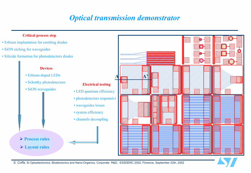
Optical transmission demonstrator
Devices
• Erbium-doped LEDs
• Schottky photodetectors
• SiON waveguidesElectrical testing
• LED quantum efficiency
• photodetectors responsivity
• waveguides losses
• system efficiency
• channels decoupling
Process rules
Layout rules
A A’
Critical process step
• Erbium implantation for emitting diodes
• SiON etching for waveguides
• Silicide formation for photodetectors diodes
S. Coffa, Si Optoelectronics, Bioelectonics and Nano-Organics, Corporate R&D, ESSDERC 2002, Florence, September 22th, 2002
Low cost SOI for galvanic isolation
SEM top view of P-Sistructure
Silic
on
HF/IPA/H2O
6” wafer
(+) Si + 2H2O + 4h+ = SiO2 + 4H+
SiO2 + 6HF = SiF62- + 2H2O + 2H+
(-) H+ + e- = ½ H2
P-Si
Porous Si formation+ -
S. Coffa, Si Optoelectronics, Bioelectonics and Nano-Organics, Corporate R&D, ESSDERC 2002, Florence, September 22th, 2002
Selective formation of buried porous Si films for low cost SOI
Si p-
Si p+
Si p-
Si poroso
S. Coffa, Si Optoelectronics, Bioelectonics and Nano-Organics, Corporate R&D, ESSDERC 2002, Florence, September 22th, 2002
Electical and structural characterisation of oxidised porous Si layers
Poli n+
Oxidised porous Si
p-type Si
Breakdown VoltageY208080 wafer 03
-6.0E-05
-4.0E-05
-2.0E-05
0.0E+00
2.0E-05
4.0E-05
6.0E-05
-800 -600 -400 -200 0 200 400 600 800Voltage [V]
Cur
rent
[A]
grande medio piccolo
S. Coffa, Si Optoelectronics, Bioelectonics and Nano-Organics, Corporate R&D, ESSDERC 2002, Florence, September 22th, 2002
Schottky photodetetors: structural and electrical characterisations
1.E-10
1.E-09
1.E-08
1.E-07
1.E-06
1.E-05
1.E-04
0 2 4 6 8 10 12 14 16
Voltage [V]C
urre
nt [
A]
darkambient lightweak white lightintens e near infrared light
Pt silicide
Field oxideN+ contact
N- well
P+ guard ring
X-SEM
X-TEM
190 Å
S. Coffa, Si Optoelectronics, Bioelectonics and Nano-Organics, Corporate R&D, ESSDERC 2002, Florence, September 22th, 2002
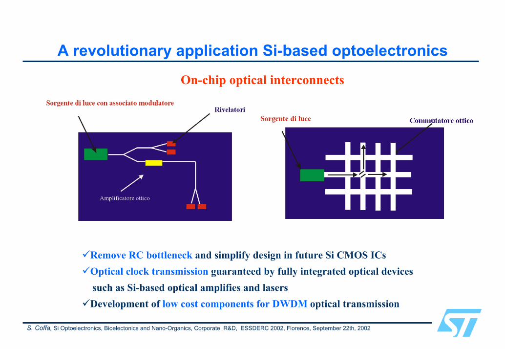
A revolutionary application Si-based optoelectronics
On-chip optical interconnects
Remove RC bottleneck and simplify design in future Si CMOS ICsOptical clock transmission guaranteed by fully integrated optical devicessuch as Si-based optical amplifies and lasersDevelopment of low cost components for DWDM optical transmission
S. Coffa, Si Optoelectronics, Bioelectonics and Nano-Organics, Corporate R&D, ESSDERC 2002, Florence, September 22th, 2002
Design and fabrication of photonic bandgap materials
S. Coffa, Si Optoelectronics, Bioelectonics and Nano-Organics, Corporate R&D, ESSDERC 2002, Florence, September 22th, 2002
Structures for photonic bandgap materials (1/2)
The silicon “Temple” Valley
Using these structure full control of light flux can be achievedand ultra-compact optical devices can be fabricated
S. Coffa, Si Optoelectronics, Bioelectonics and Nano-Organics, Corporate R&D, ESSDERC 2002, Florence, September 22th, 2002
Structures for photonic bandgap materials (2/2) Use of advanced optical lithography instead of e-beam lithography
SiO2
Si
A light splitter using 0.18 um holes in Si
S. Coffa, Si Optoelectronics, Bioelectonics and Nano-Organics, Corporate R&D, ESSDERC 2002, Florence, September 22th, 2002
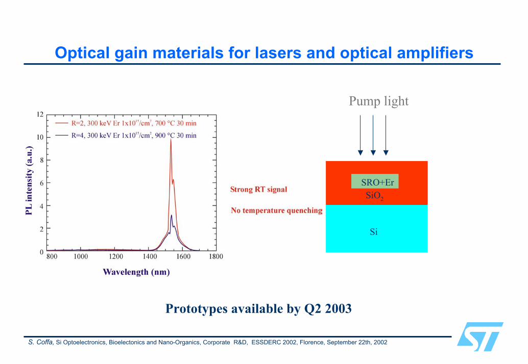
Optical gain materials for lasers and optical amplifiers
Si
SiO2
SRO+Er
Pump light
Prototypes available by Q2 2003
S. Coffa, Si Optoelectronics, Bioelectonics and Nano-Organics, Corporate R&D, ESSDERC 2002, Florence, September 22th, 2002
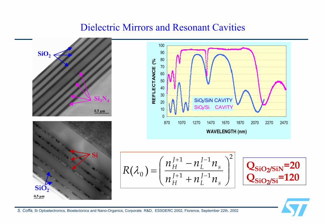
Dielectric Mirrors and Resonant Cavities
SiO2
Si3N4
0102030405060708090
100
870 1070 1270 1470 1670 1870 2070 2270 2470
WAVELENGTH (nm)
RE
FL
EC
TA
NC
E (
%)
SiO2/SiN CAVITYSiO2/Si CAVITY
Si
SiO2
2
11
11
0 )(
+−
= −+
−+
sJL
JH
sJL
JH
nnnnnn
R λ QSiO2/SiN=20QSiO2/Si=120
STMicroelectronics
Integrated Si-based optoelectronics as enabling technology in multifunctional devices
I. Biosensors
S. Coffa, Si Optoelectronics, Bioelectonics and Nano-Organics, Corporate R&D, ESSDERC 2002, Florence, September 22th, 2002
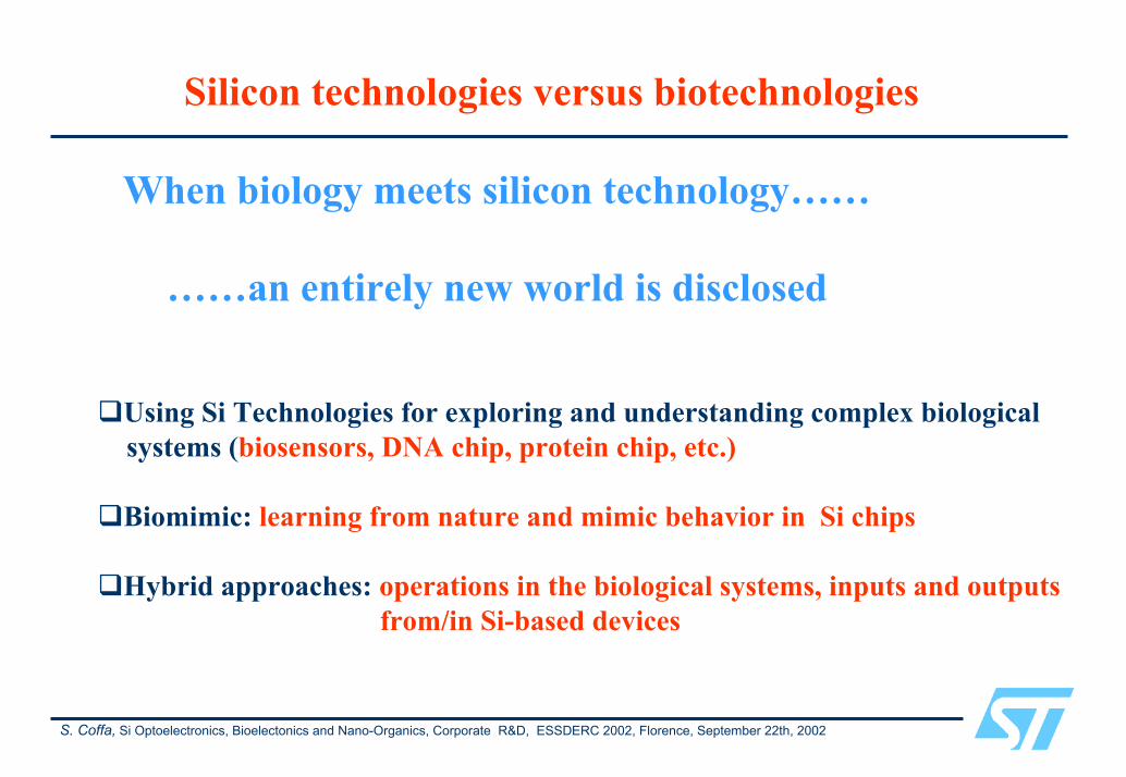
Silicon technologies versus biotechnologies
When biology meets silicon technology……
……an entirely new world is disclosed
Using Si Technologies for exploring and understanding complex biological systems (biosensors, DNA chip, protein chip, etc.)
Biomimic: learning from nature and mimic behavior in Si chips
Hybrid approaches: operations in the biological systems, inputs and outputsfrom/in Si-based devices
S. Coffa, Si Optoelectronics, Bioelectonics and Nano-Organics, Corporate R&D, ESSDERC 2002, Florence, September 22th, 2002
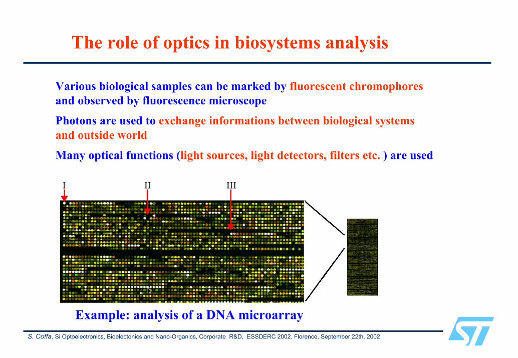
The role of optics in biosystems analysis
Various biological samples can be marked by fluorescent chromophoresand observed by fluorescence microscope
Photons are used to exchange informations between biological systems and outside world
Many optical functions (light sources, light detectors, filters etc. ) are used
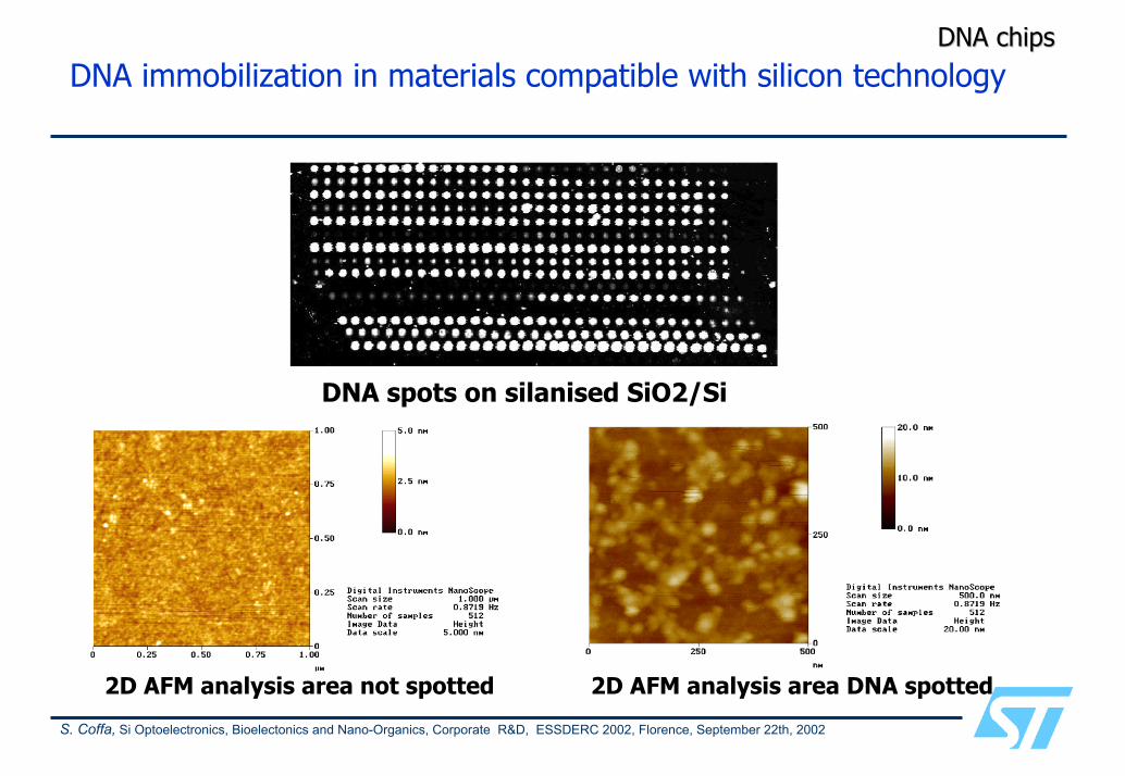
Example: analysis of a DNA microarray
S. Coffa, Si Optoelectronics, Bioelectonics and Nano-Organics, Corporate R&D, ESSDERC 2002, Florence, September 22th, 2002
Innovative silicon technologies meet biology
Optical and mechanical functions bridge the gap between Si technology and biological worldWe are able to integrate these functions with Si electronic functions on the same chip
Si electronics
Si optoelectronics
Si mechanicsBiological systems
S. Coffa, Si Optoelectronics, Bioelectonics and Nano-Organics, Corporate R&D, ESSDERC 2002, Florence, September 22th, 2002
It is the study of the patterns of gene It is the study of the patterns of gene expression in various environmental expression in various environmental circumstancescircumstances
Parallel genetic analysis allow to understand:Parallel genetic analysis allow to understand:Candidate genes for each disease (comparing Candidate genes for each disease (comparing
healthy and sick cells)healthy and sick cells)
Cellular differentiation (comparing different Cellular differentiation (comparing different tissues or the same one in different stage of tissues or the same one in different stage of development)development)
How organisms function in response to exposure How organisms function in response to exposure to environmental toxicants or other stimuli to environmental toxicants or other stimuli (elucidating the molecular mechanism that underlie (elucidating the molecular mechanism that underlie them)them)
S. Coffa, Si Optoelectronics, Bioelectonics and Nano-Organics, Corporate R&D, ESSDERC 2002, Florence, September 22th, 2002
S. Coffa, Si Optoelectronics, Bioelectonics and Nano-Organics, Corporate R&D, ESSDERC 2002, Florence, September 22th, 2002
ORGANIC COMPOUNDSORGANIC COMPOUNDS--based MATERIALS for Optical Memoriesbased MATERIALS for Optical Memories
SpirobenzopyransSpirobenzopyrans
Bit patterns read by near IR-Microscopy: (a) first layers; (b) second layer. The bit interval is 5 µm and the layers distance is 70 µm. Write by 2 photons.
Chem.Rev., 2000, 100, 1777
S. Coffa, Si Optoelectronics, Bioelectonics and Nano-Organics, Corporate R&D, ESSDERC 2002, Florence, September 22th, 2002
Biological molecules integrated within a Si chip
Novel optical memory and switches using photochromic biological molecules
hν
Photons allow communication between Si and the protein
•A red photon is used to change the colour•A blue photon can be used to switch back or to interrogate the status
S. Coffa, Si Optoelectronics, Bioelectonics and Nano-Organics, Corporate R&D, ESSDERC 2002, Florence, September 22th, 2002
Bacteriorhodopsin photocycle
(yellow)
(Purple)
S. Coffa, Si Optoelectronics, Bioelectonics and Nano-Organics, Corporate R&D, ESSDERC 2002, Florence, September 22th, 2002
Proteins with a simpler photo-cycle (e.g. Euglena-rhodopsin, GFP)
•Fast switch between the states•Single photon switch•High density•Infinite cicling
Advantages for optical memories
Special features•Superior performances compared to organic photochromic materials•Use of integrated Si optics•Protein properties can be changed using biotechnology
S. Coffa, Si Optoelectronics, Bioelectonics and Nano-Organics, Corporate R&D, ESSDERC 2002, Florence, September 22th, 2002
PROTEINSPROTEINS--based MATERIALS for Optical Memoriesbased MATERIALS for Optical Memories
NESTNEST--INFM patentINFM patent
ModifiedModified--GFP GFP (E(E22GFP)GFP)
S. Coffa, Si Optoelectronics, Bioelectonics and Nano-Organics, Corporate R&D, ESSDERC 2002, Florence, September 22th, 2002
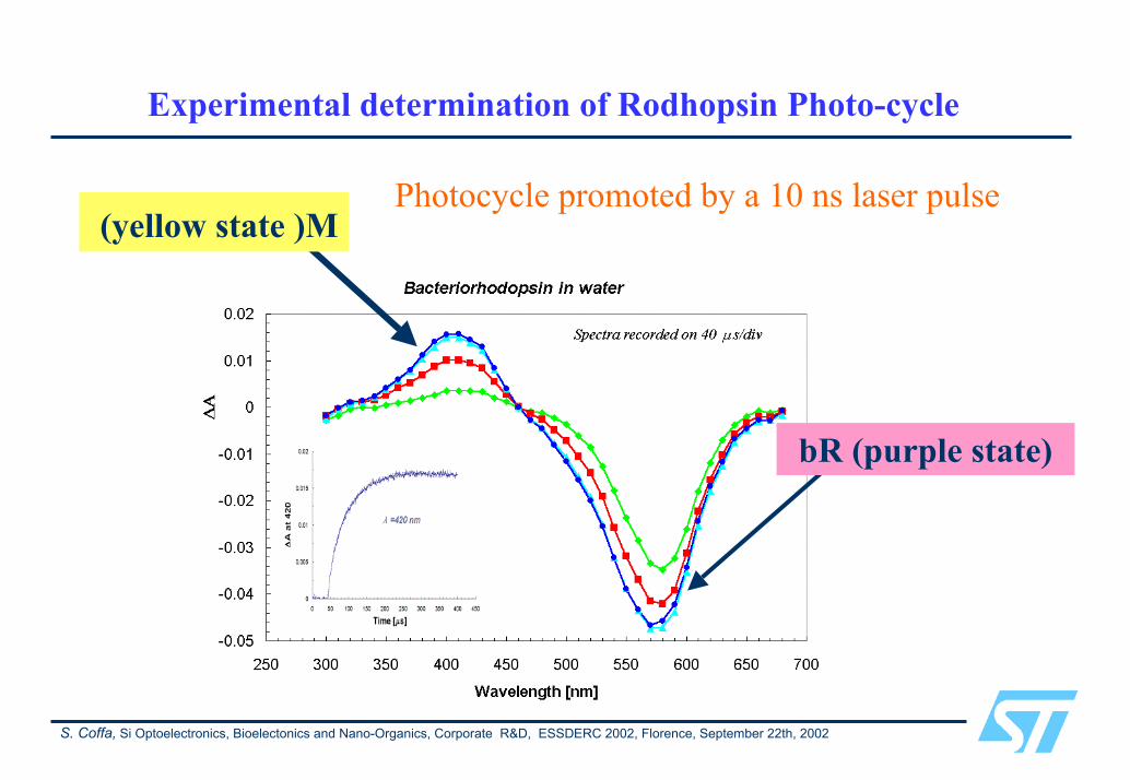
Experimental determination of Rodhopsin Photo-cycle
(yellow state )M
bR (purple state)
Photocycle promoted by a 10 ns laser pulse
S. Coffa, Si Optoelectronics, Bioelectonics and Nano-Organics, Corporate R&D, ESSDERC 2002, Florence, September 22th, 2002
Formation of the M state
300 350 400 450 500 550 600 650 700-0,030
-0,025
-0,020
-0,015
-0,010
-0,005
0,000
0,005
0,010
0,015
23ma0209
2 µs 7 µs 20 µs 80 µs
∆A
W avelength / nm
Bacterio-rodhopsin in a PAA film
S. Coffa, Si Optoelectronics, Bioelectonics and Nano-Organics, Corporate R&D, ESSDERC 2002, Florence, September 22th, 2002
50x
STRUCTURAL PERFORMANCES Active bR filmsSTRUCTURAL PERFORMANCES Active bR filmsMemoriesMemories
50x
Optical micrography bR film on glass (casting)
Optical micrography bR film on glass (casting) + 5% glycerol
S. Coffa, Si Optoelectronics, Bioelectonics and Nano-Organics, Corporate R&D, ESSDERC 2002, Florence, September 22th, 2002
Combine integrated optics and photochromic moleculesto develop innovative devices
S. Coffa, Si Optoelectronics, Bioelectonics and Nano-Organics, Corporate R&D, ESSDERC 2002, Florence, September 22th, 2002
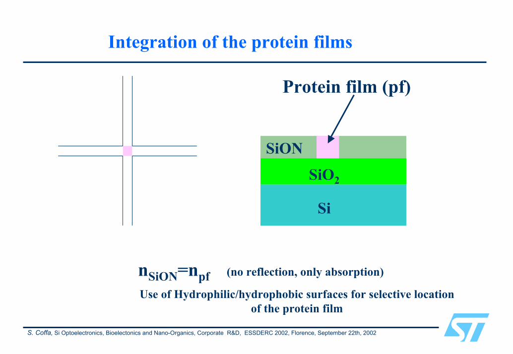
Integration of the protein films
Si
SiO2
SiON
Protein film (pf)
nSiON=npf (no reflection, only absorption)
Use of Hydrophilic/hydrophobic surfaces for selective locationof the protein film
S. Coffa, Si Optoelectronics, Bioelectonics and Nano-Organics, Corporate R&D, ESSDERC 2002, Florence, September 22th, 2002
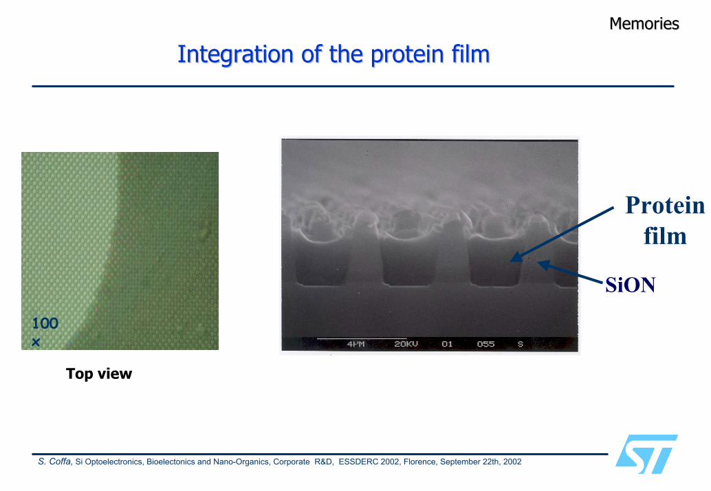
MemoriesMemories
Integration of the protein filmIntegration of the protein film
100x
Proteinfilm
SiON
Top view
S. Coffa, Si Optoelectronics, Bioelectonics and Nano-Organics, Corporate R&D, ESSDERC 2002, Florence, September 22th, 2002
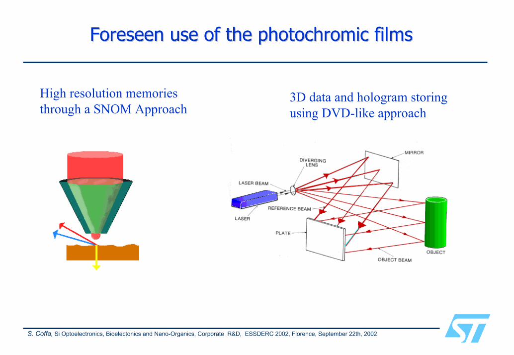
Foreseen use of the photochromic filmsForeseen use of the photochromic films
High resolution memories through a SNOM Approach
3D data and hologram storing using DVD-like approach
S. Coffa, Si Optoelectronics, Bioelectonics and Nano-Organics, Corporate R&D, ESSDERC 2002, Florence, September 22th, 2002
S. Coffa, Si Optoelectronics, Bioelectonics and Nano-Organics, Corporate R&D, ESSDERC 2002, Florence, September 22th, 2002
ConclusionsConclusions
State of the art of Si-based optical devices have been fabricated
Marketable applications of integrated Si-based optoelectronic circuits
are foreseen
Integrated Si-based optoelectronics is a suitable enabling technology
for several multifunctional devices
S. Coffa, Si Optoelectronics, Bioelectonics and Nano-Organics, Corporate R&D, ESSDERC 2002, Florence, September 22th, 2002
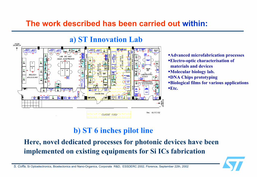
The work described has been carried out within:
Advanced microfabrication processesElectro-optic characterisation of materials and devicesMolecular biology lab.DNA Chips prototypingBiological films for various applicationsEtc.
STinnovation Labsa) ST Innovation Lab
b) ST 6 inches pilot lineHere, novel dedicated processes for photonic devices have been implemented on existing equipments for Si ICs fabrication
S. Coffa, Si Optoelectronics, Bioelectonics and Nano-Organics, Corporate R&D, ESSDERC 2002, Florence, September 22th, 2002
The work described has been carried out by:
Si optoelectronics, bioelectronicsand nano-organics group (50 people)
Corporate R&D, STMicroelectronics
Pilot line technologies and New Power Device Structure groups (10 people)
DSG R&D, STMicroelectronics
Established collaborations:CNR-IMM, CNR-IBFSNC, CIB Trieste