. . . MI) OP-44 HIGH -SPEED, PRECISION OPERATIONAL AMPLIFIER (AVCL;'::: 3) Precision Monolithics Inc. FEATURES . Slew Rate 100V/~Min . Gain-Bandwidth Product. . . . . . . . . . . . . . . . . . .. 15MHz Min . Common-ModeRejection 86dBMin . Open-LoopGain 500V/mVMin . Offset Voltage. . . . .. . . . .. . .. . .. . .. . . . . . . . . . .750/lV Max . BiasCurrent 200pAMax . Excellent AC CMR and PsR . Radiation Hard Plastic Mini-Dip and SOIC to be announced. . For devices processed in total compliance to MIL-STD-883, add /883 after part number. Consult factory for 883 data sheet. t Burn-in is available on commercial and industrial temperature range parts in cerdip, plastic dip, and TO-can packages. For ordering information, see 1988 Data Book, Section 2. GENERAL DESCRIPTION The OP-44 is a fast precision JFET-input operational amplifier delivering a 120V//ls typical slew rate in closed-loop gains of three or more. Full-power bandwidth is 2MHz for a 20Vp_p sine-wave, and 4MHz for a 10Vp_p signal. Gain-bandwidth product is typically 23M Hz. Settling time to 0.1% is 200ns, and to SIMPLIFIED SCHEMATIC +IN -IN NU~~ 111 NU~~ 151 12 bits (0.01%) is 800ns, typical. Wideband noise is minimized by only 12nV/$z flatband noise. Excellent DC precision makes the OP-44 unique among high- speed amplifiers. Offset voltage below 750/lV and 10/lV/oC maximum drift eliminates the need for external nulling poten- tiometers in most applications. Common-mode rejection of 86dB minimum and an open-loop gain of 500V/mV ensures high linearity. Errors due to bias current are virtually eliminated with the OP-44's 200pA maximum input current. PIN CONNECTIONS 8-PIN HERMETIC DIP (Z-Suffix) --' ~3uu~ zzzzz u ,. u j u z Z:J Z Z N.C. 8 NULL S 7 v+ -IN 2 6 OUT +IN 3 5 NULL 4 V- (CASEI TO-99 (J-suffix) 20-CONTACT HERMETIC LCC (RC-Suffix) V+ VOUT V- 10/87, Rev. B1 -- ORDERING INFORMATIONt TA = 2SoC PACKAGE OPERATING Vas MAX HERMETIC TEMPERATURE (mV) TO-99 DIP LCC RANGE 1.00 OP44AJ" OP44AZ" OP44ARC/883" MIL 0.75 OP44EJ OP44EZ - IND 1.50 OP44FJ OP44FZ IND OBSOLETE
.For devices processed in total compliance to MIL-STD-883, add /883 after
part number. Consult factory for 883 data sheet.t Burn-in is available on commercial and industrial temperature range parts in
cerdip, plastic dip, and TO-can packages. For ordering information, see 1988Data Book, Section 2.
GENERAL DESCRIPTION
The OP-44 is a fast precision JFET-input operational amplifierdelivering a 120V//ls typical slew rate in closed-loop gains of
three or more. Full-power bandwidth is 2MHz for a 20Vp_psine-wave, and 4MHz for a 10Vp_p signal. Gain-bandwidthproduct is typically 23M Hz. Settling time to 0.1% is 200ns, and to
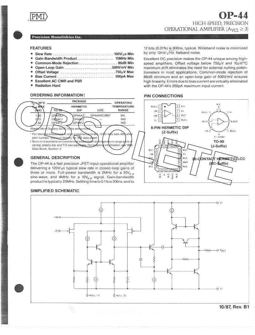
SIMPLIFIED SCHEMATIC
+IN
-IN
NU~~ 111 NU~~ 151
12 bits (0.01%) is 800ns, typical. Wideband noise is minimizedby only 12nV/$z flatband noise.
Excellent DC precision makes the OP-44 unique among high-speed amplifiers. Offset voltage below 750/lV and 10/lV/oCmaximum drift eliminates the need for external nulling poten-tiometers in most applications. Common-mode rejection of86dB minimum and an open-loop gain of 500V/mV ensureshigh linearity. Errors due to bias current are virtually eliminatedwith the OP-44's 200pA maximum input current.
Applications for the OP-44 include data acquisition systems,pulse amplifiers, RF, IF and video amplifiers, and signalgenerators.
The OP-44 conforms to the standard 741 pinout with nulling toV-. It offers an excellent upgrade for circuits using the LF400and AD509. The HA-2520/22/25 are easily upgraded by re-moving any external nulling components.
For a unity-gain stable amplifier sharing many of the OP-44'scharacteristics, consult the OP-42 data sheet.
ABSOLUTE MAXIMUM RATINGS (Note 1)
Supply Voltage :!:20VInternal Power Dissipation (Note 3) . . . . . . . . . . . . . . . . .500mWInput Voltage (Note 2) :!:20VDifferential Input Voltage (Note 2) 40VPeakOutputCurrent 50mAStorage Temperature Range. . . . . . . . . . . . . .. -65°C to 175°C
Operating Temperature RangeOP-44A(J,Z) -55°Cto+125°COP-44E,F(J,Z) -25°Cto+85°C
Junction Temperature. . . . . . . . . . . . . . . . . . . . . -65°C to 175°CLead Temperature Range (Soldering, 60 sec) 300°CNOTES:1. Absolute maximumratings apply to both DICEand packaged parts, unless
otherwise noted.2. Forsupply voltages less than i:20V,the absolute maximum input voltage is
equal to the supply voltage.3. See table for maximumambient temperature and derating factor.
t
PACKAGE TYPE
TO-99 (J)
MAXIMUMAMBIENT DERATE ABOVETEMPERATURE MAXIMUM AMBIENT
FOR RATING TEMPERATURE
80°C 7.1mW/oC
6.7mWrCHermetic 8-Pin DIP (Z)
Hermetic 20-Contact LCC (RC)
75°C
72°C 7.8mW/oC
PARAMETEROP-44E
MIN TYP MAX
ELECTRICAL CHARACTERISTICS at Vs =:!:15V,TA= 25°C, unless otherwise noted.
OP-44AMIN TYP MAXSYMBOL CONDITIONS
Offset Voltage Vos
Is VCM = OV T, = 25°C
VCM = OV T, = 25°C
Input Bias Current
Input Offset Current los
Input Voltage Range IVR (Note 1)+12.5
-12.0:':11
Common-Mode
RejectionCMR VCM = :':11V 86
Power-Supply
Rejection RatioPSRR Vs = :':10V
to :':20V
RL = 10k!l
RL = 2k!l Vo = :':10V
RL=lk!l Ti=25°C
500
200
100
Large-Signal
Voltage GainAyO
Output Voltage
Swing:':11.5
+12.5
-11.9
+33
-28
Vo RL=1kfl
Output
Current lOUT :':20
Supply CurrentNo Load
Vo = OV
RL = 2k!l
CL = 50pF100
ISY
Slew Rate SR
Full-Power
BandwidthVo = :':10V
(Note 2)
Ay= 10
(Note 3)
BWp 1.5
Gain-Bandwidth
Product15GBW
Settling Time10V Step 0.1%
(Note 4)
Vo = :':200mV
(Note 3, 4)
ts
Rise Time t,
Overshoot Vo = :':200mV
(Note 3, 4)
Overload RecoveryTime tOR
Capacitive Load
Drive Capability
AYCL 2: 3
(Note 3)50CL
OP-44FMIN TYP MAX UNITS
0.3
80
0.40.75
200
1.5
250
0.3 mV1.0
200 pA
pA
130
6
80
4 40 50 4 40
:':11+12.5
-12.0:':11
+12.5
-12.0v
96 80 .92 86 96 dB
9 40 12 50 9 40 p.V/V
900
260
170
900
260
170
V/mV
500
200
100
500
200
100
900
260
170
:':11.5+12.5
-11.9
+33
-28mA
+12.5
-11.9:':11.5 V
+33
-28:':20 :':20
6.5 7.5 6.5 mA7.5 6.5 7.5
120 80 100 V/p.s100 120
2.0 1.2 1.6 MHz1.5 2.0
23 15 23 MHz15 23
0.2 0.2p.s0.2
25 25 ns5050 25 50
25 40 25 %50 25 40
700 700 ns700 .150 50pF
150 50 150
2 10/87, Rev. 81
OBSOLETE
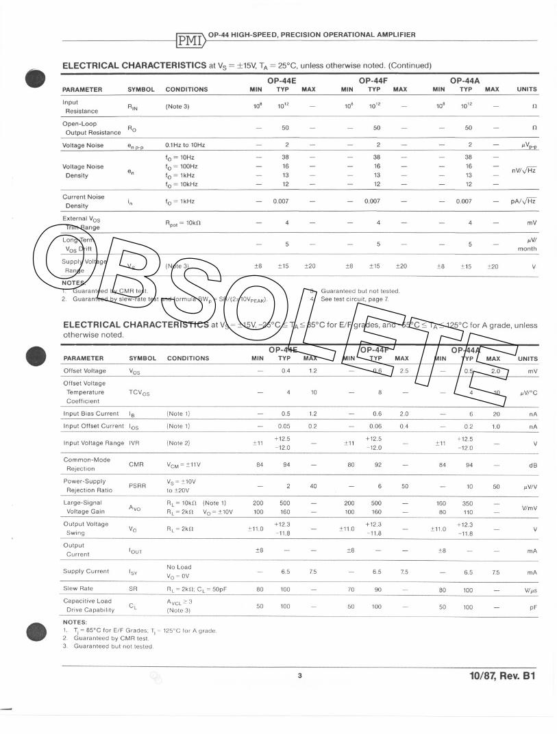
M OP-44 HIGH-SPEED,PRECISIONOPERATIONALAMPLIFIER. ELECTRICAL CHARACTERISTICS at Vs= :!::15V,TA= 25°C, unless otherwise noted. (Continued)
OP-44E OP-44F OP-44APARAMETER SYMBOL CONDITIONS MIN TYP MAX MIN TYP MAX MIN TYP MAX UNITS
NOTES:1. Guaranteed by CMR test. 3. Guaranteed but not tested.2. Guaranteed by slew-rate test and formula BWp= SR/(21T10VpEAK)' 4. See test circuit, page 7
ELECTRICAL CHARACTERISTICS at Vs = ::t15V, -25°C::; TA::; 85°C for ElF grades, and -55°C::; TA::; 125°C for A grade, unlessotherwise noted.. OP-44E OP-44F OP-44APARAMETER SYMBOL CONDITIONS MIN TYP MAX MIN TYP MAX MIN TYP MAX UNITS
Offset Voltage Vos - 0.4 1.2 - 0.6 2.5 - 0.5 2.0 mV
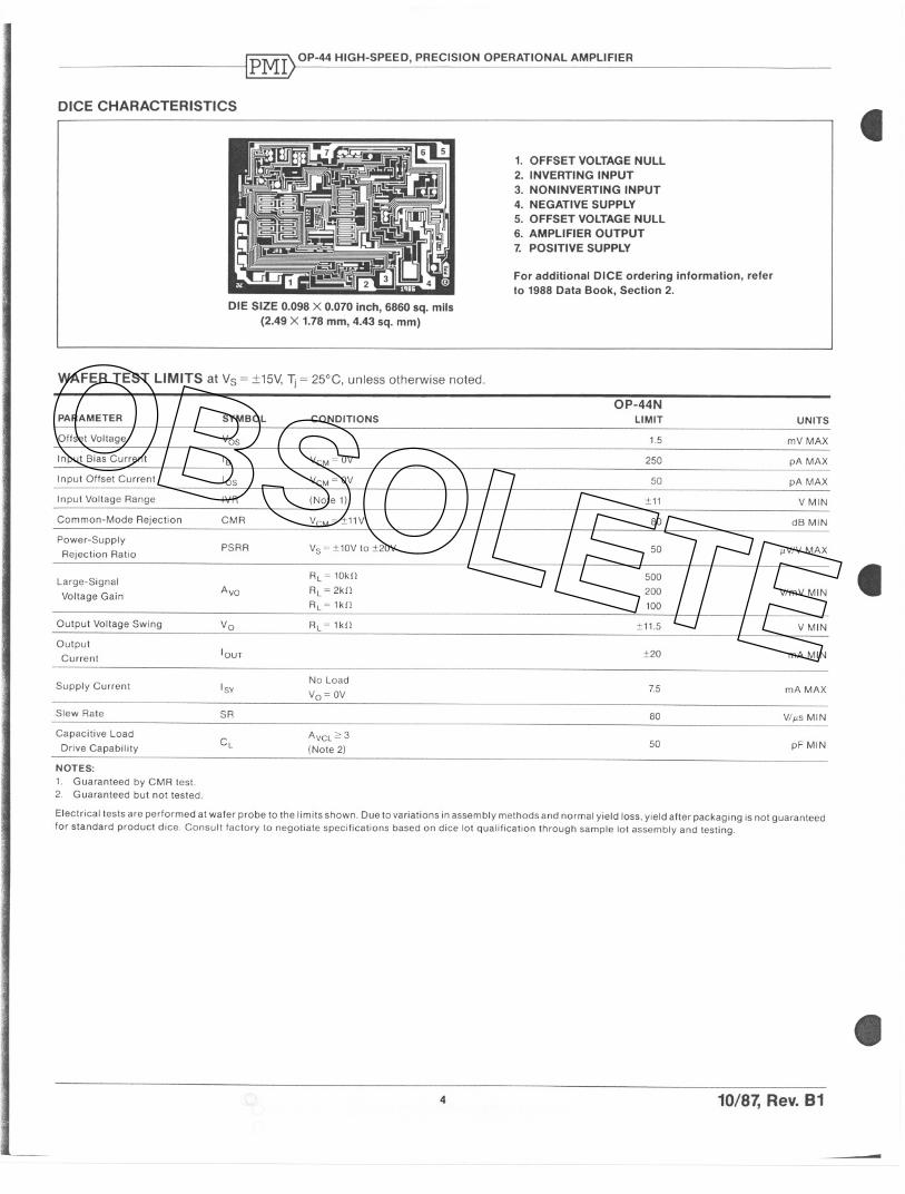
t1. OFFSET VOLTAGE NULL2. INVERTING INPUT3. NONINVERTING INPUT4. NEGATIVE SUPPLY5. OFFSET VOLTAGE NULL6. AMPLIFIER OUTPUT7. POSITIVE SUPPLY
For additional DICE ordering information, referto 1988 Data Book, Section 2.
DIE SIZE 0.098 X 0.070 inch, 6860 sq. mils(2.49 X 1.78 mm, 4.43 sq. mm)
WAFER TEST LIMITS at Vs =::t15V, 1) = 25°C, unless otherwise noted.
PARAMETER SYMBOL CONDITIONS
Offset Voltage Vas
18 VCM = OV
VCM = OV
Input Bias Current
Input Offset Current
Input Voltage Range
10S
IVR (Note 1)
Common-Mode Rejection
Power-Supply
Rejection Ratio
CMR VCM = :1:11V
PSRR Vs = :1:10V to :1:20V
Large-Signal
Voltage GainAva
RL = 10k!l
RL = 2k!l
RL=1k!l
RL = 1k!lOutput Voltage Swing
OutputCurrent
Va
lOUT
Supply Current ISYNo Load
Va = OV
Slew Rate SR
Capacitive Load
Drive CapabilityCL
AVCL 2: 3
(Note 2)
NOTES:
1. Guaranteed by CMR test.2. Guaranteed but not tested.
Electrical tests are performed at wafer probe to the limits shown. Due to variations in assembly methods and normal yield loss, yield after packaging is not guaranteedfor standard product dice. Consult factory to negotiate specifications based on dice lot qualification through sample lot assembly and testing.
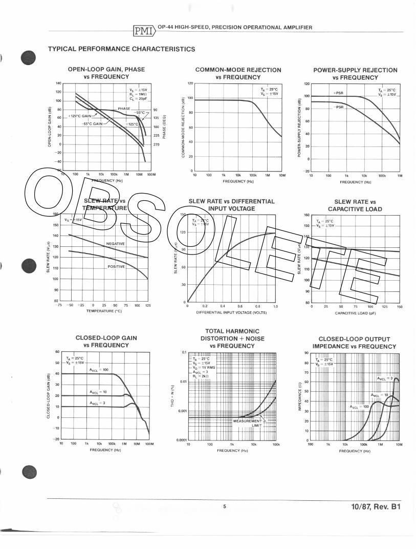
The OP-44 is a high-speed amplifier internally compensated forclosed-loop gains of 3 or more. Slew rate is typically 120V/J.ts,which allows the OP-44 output to handle a 20Vp_psine wave at2MHz. Stability is ensured by the OP-44's guaranteed capacitiveload drive ability of 50pF.
The input capacitance of high-speed op amps often causes anoticeable degradation of pulse response, resulting in exces-sive overshoot and ringing. The pole introduced by the inputcapacitance can be compensated by placing a similar capaci-tance in the feedback loop of the amplifier. For the OP-44, theinput capacitance is typically 6pF.
Small-signal and large-signal transient responses are shown inFigures 1 and 2. These photos were taken using the gain of 3test circuit shown in Figure 3.
As with most JFET-input op amps, the output of the OP-44 mayundergo phase inversion if either input exceeds the specifiedinput voltage range. Phase inversion will not damage theamplifier, nor will it cause an internal latch-up.
Supply decoupling must be used to overcome inductance andresistance associated with the supply lines to the amplifier. Formost applications, a 0.1J.tF to 0.01J.tF placed between eachsupply pin and ground is adequate. Ifsupply lines are extremelylong and/or noisy, an additional tantalum capacitor between3.3J.tFand 10J.tFshould be placed in parallel with each of thesmaller decoupling capacitors.
The OP-44 displays excellent resistance to radiation. Radiationhardness data is available by contacting the factory.
FIGURE3: Transient Response Test Circuit
V,N
SpF
VOUT
OFFSET VOLTAGEADJUSTMENTOffset voltage is adjusted with a 10kD to 100kD potentiometeras shown in Figure 4. The potentiometer is connected betweenpins 1 and 5 with its wiper connected to the V- supply. NullingVas in this manner changes TCVas by no more than 5J.tV/oCpermillivolt of Vas change. Alternately, Vas may be nulled byattaching the potentiometer wiper through a 1MD resistor to thepositive supply rail.
FIGURE4: Input Offset Voltage Nulling
V- V+
1MH
v-
v- ALTERNATE METHOD
STANDARD METHOD NOTE,
Vos CAN BE TRIMMED WITHPOTENTIOMETER RANGINGFROM 10W TO 100k!1.
Digital offset correction is possible using the nulling pins. Thecircuit of Figure 5 will correct for greater than :t4mV of offset,allowing correction of some system errors in addition to theOP-44's offset voltage. One of the four voltage-output DACs onthe PM-7226 is used to apply a voltage between OVand 10Vtothe 200kfl resistor, while the 255kfl resistor is tied to the +10Vreference. One LSB of the 8-bit PM-7226 is equivalent toapproximately 35p.V of offset change around the zero offsetpoint.
FIGURE 5: Digital Offset Correction
+15V
255kO 2ookO
REF-O1 .6
VAEF
1/4PM-7226
---DIGITALINPUT
A common problem with many high-speed amplifiers is arequirement for more DC precision than the amplifier's capa-bility. While the OP-44 already offers an order of magnitude ormore improvements in precision over previous high-speedamplifiers, some users may find a need for even greaterprecision.
Figure 6 shows a combination amplifier melding the precisionDC characteristics of an OP-97 with the high speed of theOP-44. The OP-97 reacts for low-frequency and DC signals,while the OP-44 is dominant at higher frequencies. Over-compensation of the OP-97 ensures that it operates only at lowfrequencies. Resistor matching is important to optimize thiscircuit's transient response. The overall supply current of thiscombination amplifier is only slightly higher than that of theOP-44 alone. This is due to the minimal consumption of theOP-97, only 600p.A.Transient response of this circuit is shown inFigure 7.Its initial offset voltage is 20p.V,while TCVos is less thanO.6p.V!°C.
Baseline restoration is another useful technique for correctingerrors introduced by amplifier drift, or by electromagneticpickup. High-impedance sources, such as a human body, arenotorious for large DC drifts. In many cases, where pulse or ACmeasurements are being made, and the pulse height above anominal DC line contains the important information.
While a simple high-pass filter may be adequate for somesituations, the baseline restorer shown in Figure 9 allows a widedegree of flexibility for analog adaptive filtering techniques, andoffers some benefits not available with a frequency-domainfilter.
The baseline restorer behaves as a nonlinear filter, acting uponthe slew rate of the input signal rather than its frequency. Itsoutput will restore the base of the pulses to an arbitrary level, setby VREF.The slew rate cutoff of the filter is set by the currentflowing through 01, which is in turn set by VPROGRAM.VREFandVPROGRAMmay be controlled by a voltage-output DACsuch asthe PM-7226. Ifcurrent programming is desired, RpROGRAMmaybe removed and replaced by a current-source, such as a bipolarDAC.
To understand the circuit's operation, assume that capacitor Chas charged to the DC baseline. If the output swings above thebaseline, IC2 swings low, reverse biasing diode D2. D1 is pulledlow, and forward biases. A current (12 - '1) discharges thecapacitor until equilibrium is restored. Ifthe output drops belowthe baseline, IC2 swings high, and D2 becomes forward biased.12is supplied by the output of IC2 while 11charges C until thebaseline is restored. The rate of restoration depends upon thecurrent available to charge or discharge C.
R2
2k11
R1
V'N2k11
VOUT
VREF
FIGURE 10: Baseline Restorer Response
For symmetric operation, with the same restoration rate forpositive or negative excursions from the baseline, 12must betwice '1, This provides an equal current for charging anddischarging the capacitor. 11 is set by the current flowingthrough 01 in the MAT-O4.An identical current flows througheach transistor. The MAT-O3matched PNP pair, 05 and 06, actas a current mirror to reflect the current through 02 (11).03 and04 create '2, which is twice 11.11may be set anywhere between afew nanoamps to several mA. Higher currents will result inrejection of faster-slewing signals, while lower currents willallow passage of slower signals.
The OP-44 is configured for a gain of -1, but gain is adjustableby R1 and R2, and is simply -(R2/R1). OP-44 stability is main-tained by the dominant pole introduced by C.