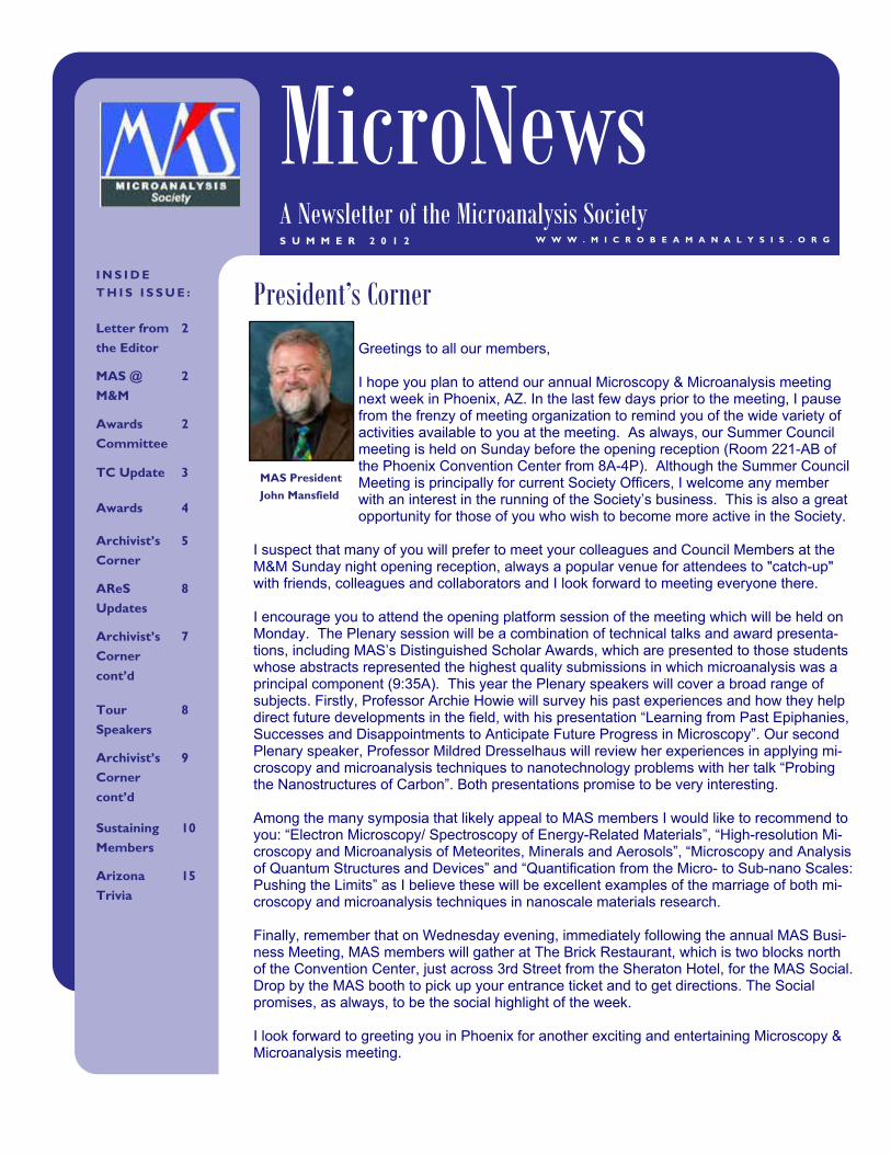
Greetings to all our members, I hope you plan to attend our annual Microscopy & Microanalysis meeting next week in Phoenix, AZ. In the last few days prior to the meeting, I pause from the frenzy of meeting organization to remind you of the wide variety of activities available to you at the meeting. As always, our Summer Council meeting is held on Sunday before the opening reception (Room 221-AB of the Phoenix Convention Center from 8A-4P). Although the Summer Council Meeting is principally for current Society Officers, I welcome any member with an interest in the running of the Society’s business. This is also a great opportunity for those of you who wish to become more active in the Society. I suspect that many of you will prefer to meet your colleagues and Council Members at the M&M Sunday night opening reception, always a popular venue for attendees to "catch-up" with friends, colleagues and collaborators and I look forward to meeting everyone there. I encourage you to attend the opening platform session of the meeting which will be held on Monday. The Plenary session will be a combination of technical talks and award presenta- tions, including MAS’s Distinguished Scholar Awards, which are presented to those students whose abstracts represented the highest quality submissions in which microanalysis was a principal component (9:35A). This year the Plenary speakers will cover a broad range of subjects. Firstly, Professor Archie Howie will survey his past experiences and how they help direct future developments in the field, with his presentation “Learning from Past Epiphanies, Successes and Disappointments to Anticipate Future Progress in Microscopy”. Our second Plenary speaker, Professor Mildred Dresselhaus will review her experiences in applying mi- croscopy and microanalysis techniques to nanotechnology problems with her talk “Probing the Nanostructures of Carbon”. Both presentations promise to be very interesting. Among the many symposia that likely appeal to MAS members I would like to recommend to you: “Electron Microscopy/ Spectroscopy of Energy-Related Materials”, “High-resolution Mi- croscopy and Microanalysis of Meteorites, Minerals and Aerosols”, “Microscopy and Analysis of Quantum Structures and Devices” and “Quantification from the Micro- to Sub-nano Scales: Pushing the Limits” as I believe these will be excellent examples of the marriage of both mi- croscopy and microanalysis techniques in nanoscale materials research. Finally, remember that on Wednesday evening, immediately following the annual MAS Busi- ness Meeting, MAS members will gather at The Brick Restaurant, which is two blocks north of the Convention Center, just across 3rd Street from the Sheraton Hotel, for the MAS Social. Drop by the MAS booth to pick up your entrance ticket and to get directions. The Social promises, as always, to be the social highlight of the week. I look forward to greeting you in Phoenix for another exciting and entertaining Microscopy & Microanalysis meeting. A Newsletter of the Microanalysis Society INSIDE THIS ISSUE: Letter from the Editor 2 MAS @ M&M 2 TC Update 3 Awards 4 Archivist’s Corner 5 AReS Updates 8 Archivist’s Corner cont’d 7 Tour Speakers 8 Archivist’s Corner cont’d 9 Sustaining Members 10 Arizona Trivia 15 Awards Committee 2 MicroNews WWW.MICROBEAMANALYSIS.ORG SUMMER 2012 President’s Corner MAS President John Mansfield
Transcript
Greetings to all our members, I hope you plan to attend our annual Microscopy & Microanalysis meeting next week in Phoenix, AZ. In the last few days prior to the meeting, I pause from the frenzy of meeting organization to remind you of the wide variety of activities available to you at the meeting. As always, our Summer Council meeting is held on Sunday before the opening reception (Room 221-AB of the Phoenix Convention Center from 8A-4P). Although the Summer Council Meeting is principally for current Society Officers, I welcome any member with an interest in the running of the Society’s business. This is also a great opportunity for those of you who wish to become more active in the Society.
I suspect that many of you will prefer to meet your colleagues and Council Members at the M&M Sunday night opening reception, always a popular venue for attendees to "catch-up" with friends, colleagues and collaborators and I look forward to meeting everyone there. I encourage you to attend the opening platform session of the meeting which will be held on Monday. The Plenary session will be a combination of technical talks and award presenta-tions, including MAS’s Distinguished Scholar Awards, which are presented to those students whose abstracts represented the highest quality submissions in which microanalysis was a principal component (9:35A). This year the Plenary speakers will cover a broad range of subjects. Firstly, Professor Archie Howie will survey his past experiences and how they help direct future developments in the field, with his presentation “Learning from Past Epiphanies, Successes and Disappointments to Anticipate Future Progress in Microscopy”. Our second Plenary speaker, Professor Mildred Dresselhaus will review her experiences in applying mi-croscopy and microanalysis techniques to nanotechnology problems with her talk “Probing the Nanostructures of Carbon”. Both presentations promise to be very interesting. Among the many symposia that likely appeal to MAS members I would like to recommend to you: “Electron Microscopy/ Spectroscopy of Energy-Related Materials”, “High-resolution Mi-croscopy and Microanalysis of Meteorites, Minerals and Aerosols”, “Microscopy and Analysis of Quantum Structures and Devices” and “Quantification from the Micro- to Sub-nano Scales: Pushing the Limits” as I believe these will be excellent examples of the marriage of both mi-croscopy and microanalysis techniques in nanoscale materials research. Finally, remember that on Wednesday evening, immediately following the annual MAS Busi-ness Meeting, MAS members will gather at The Brick Restaurant, which is two blocks north of the Convention Center, just across 3rd Street from the Sheraton Hotel, for the MAS Social. Drop by the MAS booth to pick up your entrance ticket and to get directions. The Social promises, as always, to be the social highlight of the week. I look forward to greeting you in Phoenix for another exciting and entertaining Microscopy & Microanalysis meeting.
A Newsletter of the Microanalysis Society
I N S I D E
T H I S I S S U E :
Letter from
the Editor
2
MAS @
M&M
2
TC Update 3
Awards 4
Archivist’s
Corner
5
AReS
Updates
8
Archivist’s
Corner
cont’d
7
Tour
Speakers
8
Archivist’s
Corner
cont’d
9
Sustaining
Members
10
Arizona
Trivia
15
Awards
Committee
2
MicroNews W W W . M I C R O B E A M A N A L Y S I S . O R G S U M M E R 2 0 1 2
President’s Corner
MAS President
John Mansfield
P A G E 2
Sunday MAS Council Meeting, 8A, 221AB
Monday MAS Awards Presentation, 9:35A, North 120CD Ballroom
MAS Meal With A Mentor, 12P, 224B
Wednesday MAS Affiliated Regional Societies, 12:15P, 224B
MAS Business Meeting, 5:15P, 121BC
MAS Social, 6:30P, Stop by the MAS booth to update con-tact information, renew membership, and receive ticket to the Social
MAS @ M&M
Letter from the Editor by Heather Lowers M&M 2012 is just around the corner. This issue of MicroNews will hope-fully bring you up to date with the latest news about MAS and events at M&M. This Spring proved to be busy with two successful Topical Confer-ences, Microanalytical Reference Materials and EBSD.
To keep you further up to date with Society business, minutes from past Business Meetings and Council meetings have been posted at http://www.microanalysissociety.org/council/council‐meetings
The Editor’s term for MicroNews is over at the end of 2012. If you are interested in the position, have material to contribute, or ideas for future issues, please email the Editor at [email protected].
M I C R O N E W S
MAS Creates Awards Committee Paul Kotula will be the inaugural chair of the Awards Committee from 2011 to 2014. The Committee consists of eight members with the outgo-ing Directors serving as ex officio members. The current Awards Com-mittee is Paul Kotula, Rhonda Stroud, John Donovan, Joe Michael, Steve Claves, John Friel, Masashi Watanabe, and Raynald Gauvin. If you see a paper appropriate for one of the numerous MAS awards at the M&M meeting in Phoenix, please email the title and author name to Paul Kotula at [email protected].
Check out these excit-ing, relatively new topics at M&M
A03– TEM Phase Con-trast Imaging in Biologi-cal and Materials Sci-ence
A08—Channeling ef-fects in microscopy and microanalysis
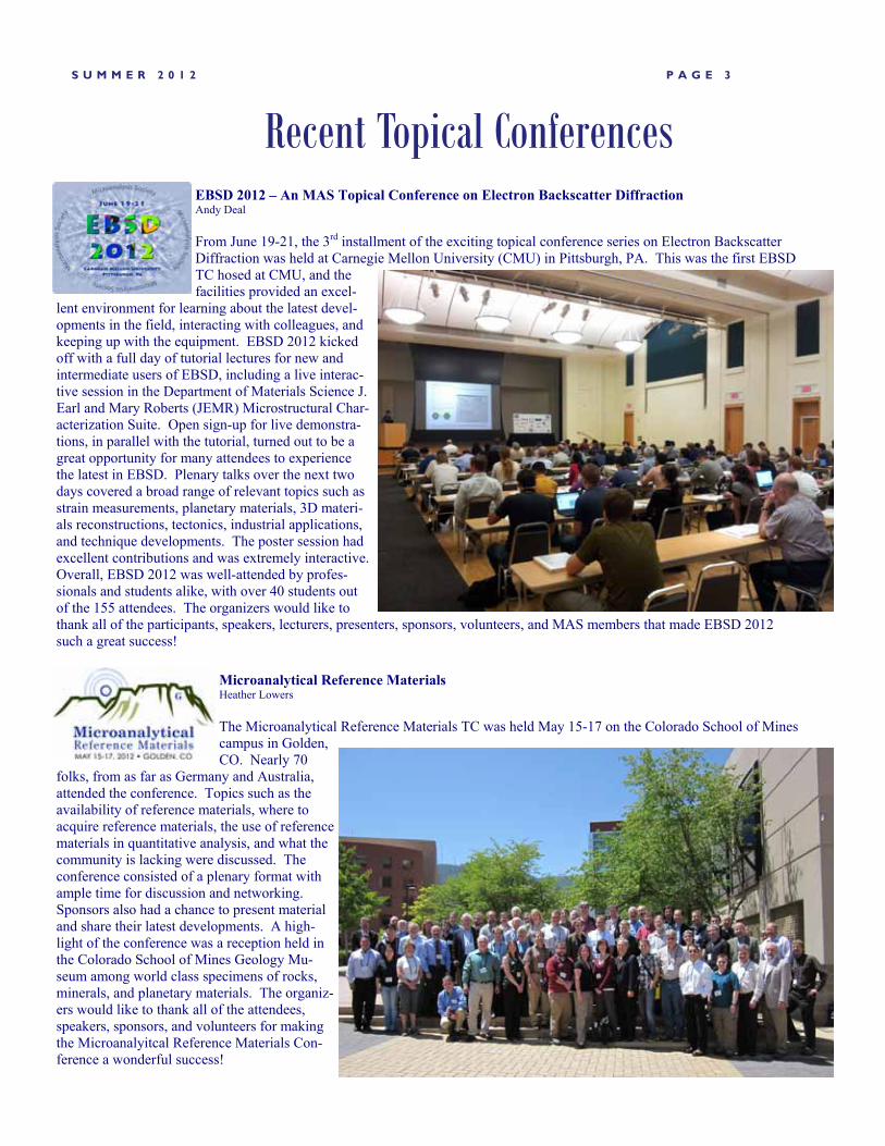
Recent Topical Conferences EBSD 2012 – An MAS Topical Conference on Electron Backscatter Diffraction Andy Deal
From June 19-21, the 3rd installment of the exciting topical conference series on Electron Backscatter Diffraction was held at Carnegie Mellon University (CMU) in Pittsburgh, PA. This was the first EBSD TC hosed at CMU, and the facilities provided an excel-
lent environment for learning about the latest devel-opments in the field, interacting with colleagues, and keeping up with the equipment. EBSD 2012 kicked off with a full day of tutorial lectures for new and intermediate users of EBSD, including a live interac-tive session in the Department of Materials Science J. Earl and Mary Roberts (JEMR) Microstructural Char-acterization Suite. Open sign-up for live demonstra-tions, in parallel with the tutorial, turned out to be a great opportunity for many attendees to experience the latest in EBSD. Plenary talks over the next two days covered a broad range of relevant topics such as strain measurements, planetary materials, 3D materi-als reconstructions, tectonics, industrial applications, and technique developments. The poster session had excellent contributions and was extremely interactive. Overall, EBSD 2012 was well-attended by profes-sionals and students alike, with over 40 students out of the 155 attendees. The organizers would like to thank all of the participants, speakers, lecturers, presenters, sponsors, volunteers, and MAS members that made EBSD 2012 such a great success!
The Microanalytical Reference Materials TC was held May 15-17 on the Colorado School of Mines campus in Golden, CO. Nearly 70
folks, from as far as Germany and Australia, attended the conference. Topics such as the availability of reference materials, where to acquire reference materials, the use of reference materials in quantitative analysis, and what the community is lacking were discussed. The conference consisted of a plenary format with ample time for discussion and networking. Sponsors also had a chance to present material and share their latest developments. A high-light of the conference was a reception held in the Colorado School of Mines Geology Mu-seum among world class specimens of rocks, minerals, and planetary materials. The organiz-ers would like to thank all of the attendees, speakers, sponsors, and volunteers for making the Microanalyitcal Reference Materials Con-ference a wonderful success!
P A G E 4 2012 Award Winners MAS Distinguished Scholar Awards
S. Avasthy, Northwestern University, Sub-cellular Dynamic Mechanical Response Measurements of Live Human Pulmonary Artery Endothelial Cells with Atomic Force Microscopy
C. Aydin, University of California-Davis, Atomic-Resolution Imaging of Zeolite-Supported Metal Complex Catalysts
N. Bailey, University of California, Berkeley, Initial APT Analysis of Irradiated MA957
P. Gopon, University of Wisconsin, Soft X-ray EPMA of Submicron Phase Lunar Fe-Si Compounds
M. E. Holtz, Cornell University, In-situ Electron Energy Loss Spectroscopy of Liquids
L. Jones, University of Oxford, United Kingdom, Focal Series Reconstruction in Annular Dark-Field STEM
J. K. Kawasaki, University of California, Santa Barbara, Growth Mechanisms and Electronic Structure of Em-bedded ErAs and ErSb Nanostructures Studied by In-Situ Scanning Tunneling Microscopy
B. K. Miller, Arizona State University, On the Fly Determination of Gas Compositions Inside an ETEM Reac-tion Cell
M. Rathi, South Dakota School of Mines & Technology, A Standards-Based Method to Determine Elemental Compositions using Energy Dispersive X-Ray Spectrometry for Compound Semiconductors
D. R. Samarajeewa, University of Texas at Dallas, Surfactant Peptide/SWNT Composites with Altered Elec-tronic Properties
R. Tao, University of Illinois at Chicago, In-situ Study of Nb Oxide and Hydride on Thin Films using Electron Energy Loss Spectroscopy
S.Y. Woo, McMaster University, Canada, Measurement of Indium-Content Variation in InGaN/GaN Dot-in-a-Wire Nanostructures by Electron Energy-Loss Spectroscopy
Presidential Service Award Cathy Johnson
Presidential Science Award Nestor J Zaluzec
K.F.J. Heinrich Award Emmanulle A Marquis
The Duncumb Award (sponsored by Bruker Nano) James Bentley
MAS Outstanding Paper Awards from the M&M2011 Meeting (to be presented in Phoenix)
Castaing Award for Best Student Paper sponsored by P. Y. Huang, A. M. van der Zande, C. S. Ruiz-Vargas, W. S. Whitney, M. P. Levendorf, J. W. Kevek, Y. Zhu, J. Park, P. L. McEuen, D. A. Muller, Cornell University Imaging Grains and Grain Boundaries in Single-Layer Graphene: An Atomic Patchwork Quilt Birks Award for Best Contributed Paper sponsored by R. R. Unocic, L. A. Adamczyk, N. J. Dudney, K. L. More, Oak Ridge National Laboratory D. H. Alsem, N. J. Salmon, Hummingbird Scientific In-situ TEM Characterization of Electrochemical Processes in Energy Storage Systems Cosslett Award for Best Invited Paper sponsored by MAS C. A. Simmons, University of Toronto, Canada Microtechnologies for Studying Cell Biology in Physiologically Relevant Microenvironments Macres Award for Best Instrumentation/Software Paper sponsored by I. Massmann, S. Uhlemann, H. Muller, P. Hartel, J. Zach, M. Haider, CEOS GmbH, Germany; Y. Taniguchi, Hitachi High-Technology Corp., Japan; D. Hoyle, Hitachi High-Technology Ltd., Canada; R. Herring, University of Victoria, Canada Realization of the First Aplanatic Transmission Electron Microscope
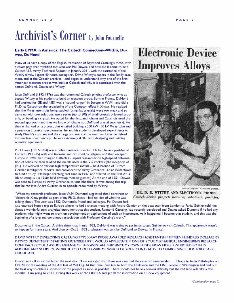
Early EPMA in America: The Caltech Connection--Wittry, Du-wez, DuMond Many of us have a copy of the English translation of Raymond Castaing’s thesis, with a cover page that mystified me: who was Pol Duwez, and how did it come to be a Caltech/U.S. Army Technical Report? In January 2011, with the assistance of the Wittry family, I spent 40 hours poring thru David Wittry’s papers in the family base-ment, and at the Caltech archives…and began to understand why one of the first American electron probes was built at Caltech and why it is associated with the names DuMond, Duwez and Wittry. Jesse DuMond (1892-1976) was the renowned Caltech physics professor who ac-cepted Wittry as his student to build an electron probe. Born in France, DuMond had worked for GE and NBS, was a “sound ranger” in Europe in WW1, and did a Ph.D. at Caltech on the broadening of the Compton effect in X-rays. He realized that the X-ray intensities being studied (using flat crystals) were too weak and so came up with two solutions: use a series (up to 50!) of small crystals oriented prop-erly, or bending a crystal. He opted for the first, and Johann and Cauchois used the second approach (and thus we know of Johann not DuMond crystal geometry). He then embarked on a project that entailed building a 300 kW 100 kV X-ray tube and a precision 2 crystal spectrometer; he and his students developed experiments to study Planck’s constant and the charge and mass of the electron. Later he delved into nuclear spectroscopy. He was extremely skillful with designing and building scientific equipment. Pol Duwez (1907-1984) was a Belgian material scientist. He had been a postdoc at Caltech (1933-35) with von Karman, and returned to Belgium, and then escaped Europe in 1940. Returning to Caltech as unpaid researcher on high-speed deforma-tion of solids, he then studied the metals used in the V-2 rockets (the inception of JPL.) He worked on various high temperature metals -- he’d learned of Ti from German intelligence reports, and convinced the Army Ordnance Lab at Watertown to fund a study. He began teaching part time in 1947, and started up the first XRD lab on campus. (In 1960s he’d develop metallic glasses.) At the end of 1951, Duwez was sent to Europe by Army Ordnance to visit labs there. It was during this trip that he ran into Andre Guinier, in an episode recounted by Wittry: “When my research professor, Jesse W.M. Dumond suggested that I construct an ‘electronic X-ray probe’ as part of my Ph.D. thesis, I had no idea of what he was talking about. The year was 1952. Dumond’s friend and colleague, Pol Duwez had just returned from a trip to Europe where he had a chance meeting with Andre Guinier on the boat train from London to Paris. Guinier told him about a wonderful new analytical instrument that this student, Raimond Castaing, had recently developed and Duwez asked Dumond if he had any students who might want to work on development or applications of such an instrument. As it happened, I became that student, and this was the beginning of a long and continuous association with Professor Castaing’s work.” Documents in the Caltech Archive show that in mid 1952, DuMond was trying to get funds to get Guinier to visit Caltech. This apparently wasn’t to happen for many years. And then on Oct 3, 1952 a telegram was sent by DuMond to Duwez (in France): DAVID WITTRY DEVELOPING CASTAING TYPE X-RAY PROBE AWARDED RESEARCH ASSISTANTSHIP FIFTEEN HUNDRED DOLLARS BY PHYSICS DEPARTMENT STARTING OCTOBER FIRST. WOULD APPRECIATE IF ONE OF YOUR MECHANICAL ENGINEERING RESEARCH CONTRACTS COULD ASSUME EXPENSE OF THIS ASSISTANTSHIP SINCE MY OWN FUNDS NOW MORE RESTRICTED BOTH IN AMOUNT AND SCOPE OF WORK. IF YOU COULD WIRE ME WHICH OF YOUR CONTRACTS TO CHARGE SINCE DOCTOR CLARK UNCERTAIN. Duwez sent off an airmail letter the next day: “I am very glad that Dave was awarded the research assistantship. … I hope to be in Philadelphia on Oct 24 for the meeting of the Am Inst of Met Eng. At that time I will talk to both the Ordnance and the ONR people in Washington and find out the best way to obtain a sponsor for the project as soon as possible. There should not be any serious difficulty but the red tape will take a few months. I am going to visit Castaing this week at the ONERA and get all the information on his new equipment.”
(Continued on page 7)
Appalachian Regional Microscopy Society next AReMS meeting: October 11 & 12, 2012, Knoxville, TN
The Midwest Microscopy and Microanalysis Society, an affiliate of both MAS and MSA, is one of the oldest and largest Affiliated Societies. Their winter meeting, “Microscopy for Life: M3S Celebrates 55 Years” will be held November 15, 2012 at Baxter Healthcare, Deerfield, IL.
The 12th Biennial Australian Microbeam Analysis Society Symposium will be held in Sydney, NSW, Australia at the University of Technology, Sydney, in Cen-tral Sydney. 4-8 Feb 2013
Oklahoma Microscopy Society will hold the 2012 Fall Technical Meeting in con-junction with the 101st Annual Technical Meeting of the Oklahoma Academy of Science on Friday, November 9, 2012, at University of Central Oklahoma in Edmond. OMS will have a number of talks, one keynote speaker and the compe-tition for the 2012 Timpano Award for the best student presentation.
P A G E 6
Upcoming AReS Meetings
M I C R O N E W S
20 Years After Chuck - A Memorial Symposium Friday, September 14, 2012 1-4 pm
NIST, Gaithersburg, MD
The Mid-Atlantic Microbeam Analysis Society is proud to present “20 Years After Chuck: Progress in Microbeam Analysis along Fiori’s Trajectories,” a half day symposium on the advances over the last 20 years that would have interested our dearly departed friend and colleague Chuck Fiori, an Honorary Member of MAS. It will be held on Friday, September 14, 2012, from 1-4 pm at the NIST campus in Gaithersburg, MD. We will start off with a welcome from Dr. John Small, Chief of the NIST Surface and Microanalysis Science Divi-sion and continue with talks by Dale Newbury (NIST), Nicholas Ritchie (NIST), Edward Vicenzi (Smithsonian Institution) and Richard Leapman (NIH). After listening to the talks, we will retire across the street to the Dogfish Head Alehouse to raise our glasses to Chuck!
Registration is required, for more information please see http://www.microprobe.org/mid-atlantic-microbeam-analysis-society-meeting or send email to [email protected].
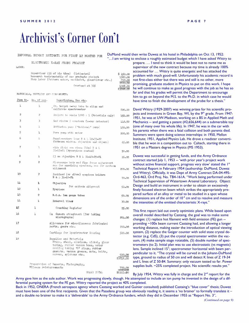
Archivist’s Corner Con’t DuMond would then write Duwez at his hotel in Philadelphia on Oct 13, 1952: “…I am writing to enclose a roughly estimated budget which I have asked Wittry to
prepare. … I tend to think it would be best not to name me as supervisor of the new contract because my time is already 100% accounted for … Wittry is quite energetic and has attacked the problem with much good-will. Unfortunately his academic record is not first-class either but there was and still is no other, more promising, graduate student in Physics to put on this work. I hope he will continue to make as good progress with the job as he has so far and that his grades will permit the Department to encourage him to go on beyond the M.S. to the Ph.D. in which case he would have time to finish the development of the probe for a thesis.” David Wittry (1929-2007) was winning prizes for his scientific pro-jects and inventions in Green Bay, WI, by the 9th grade. From 1947-1951, he was at UW-Madison, working on a BS in Applied Math and Mechanics -- and getting a patent (#2,656,644) on a submersible toy (one of many over his whole life). In 1947, he was in the car with his parents when there was a fatal collision and both parents died. Summers were spent doing science internships: in 1950, Mellon Institute; 1951, Applied Physics Lab. He drove a roadster converti-ble that he won in a competition out to Caltech, starting there in 1951 on a Masters degree in Physics (MS 1953). Duwez was successful in getting funds, and the Army Ordnance contract started July 1, 1953 -- ‘with prior year’s project work without active financial support, progress very slow’ stated the 1st Technical Report in February 1954 (authorship: DuMond, Duwez and Wittry). Officially, it was Dept of Army Contract DA-04-495-Ord-463, Ord Proj. No. TB4-161A. “Work being performed under Technical Supervision of Watertown Arsenal Laboratory. Object: Design and build an instrument in order to obtain an excessively finely focused electron beam which strikes the appropriately pre-pared surface of an alloy or metal to be studied in a spot whose dimensions are of the order of 10-4 cm and to resolve and measure the intensities of the emitted characteristic X-rays.” This first report laid out overly optimistic plans. While based upon overall model described by Castaing, the goal was to make some changes: (1) replace hot filament with field emission (FE) gun -- providing ~100x beam current Castaing had, and allowing a longer working distance, making easier the introduction of optical viewing system, (2) replace the Geiger counter with solid state crystal de-tector (e.g. CdS), (3) put the crystal spectrometer within the vac-uum, (4) make sample stage rotatable, (5) double number of spec-trometers (to 2). Initial plan was to use electrostatic (vs magnetic) lens. Sample inclined 15°; spectrometer horizontal with beam per-pendicular to it. “The crystal will be curved in the Johann-DuMond type, ground to radius of 50 cm and will detect K lines of Z 19-34 and L lines of Z 50-84. Summary: only vacuum tested so far. Power supplies built. ~25% completed project. No scientific results yet.” By July 1954, Wittry was fully in charge and the 2nd report for the
Army gave him as the sole author. Work was progressing slowly, though. He attempted to include an ion pump he invented in the design of a dif-ferential pumping system for the FE gun. Wittry reported the project as 40% completed. Back in 1952, ONERA (French aerospace agency where Castaing worked and Guinier consulted) published Castaing’s “blue cover” thesis; Duwez must have been one of the first recipients. Given that the Pasadena group was obviously reading it, it seems a ‘no brainer’ to formally translate it – and a double no brainer to make it a ‘deliverable’ to the Army Ordnance funders, which they did in December 1955 as “Report No. 3”,
(Continued on page 9)
P A G E 8
2012 Tour Speakers
M I C R O N E W S
MAS provides interesting technical speakers for meetings of its Affiliated Regional Societies (AReS). The Tour Speaker Program is most significant tangible benefit that MAS provides to its AReS. This program provides annually at no charge to each AReS a renowned speaker for one of their technical meetings. Moreover, the pool of speakers – typically a choice of three – is cho-sen by representatives of the AReS at the annual meeting, thus ensuring that the subject matter of the speakers is highly relevant to the AReS membership.
The 2012 MAS Tour Speakers and the titles of their talks are shown below. Last year's MAS Tour Speakers are also available through the end of the year. Remember that all arrangements by Affiliated Regional Societies for Tour Speakers must be made through the MAS AReS Direc-tor.
All You Ever Wanted to Know about Silicon Drift Detectors (but Were Afraid to Ask) Richard McLaughlin Oxford Instruments Concord, MA
How the Sausage is Made: A Microanalyst's Time in the White House John Henry Scott NIST Gaithersburg, MD
Reflections on Microscopy & Analysis: From Viewing the Small World to Leading on a Larger Stage Dave Williams The Ohio State University Columbus, OH
More From The Archives by John Fournelle P A G E 9 S U M M E R 2 0 1 2
“Application of electron probes to local chemical and crystallographic analysis”, by Castaing and translated by Duwez and Wittry. By December 1955, Duwez and Wittry reported 70% progress in the project (Report No 4). In it they described in detail the complications in-volved with FE* emitters, and then give a detailed ‘cook book’ procedure for production of them. Pulsed currents seemed to be required, and they raised questions about possible issues with thermal effects in the samples. They scaled down the improvement in beam current vs Castaing now to 10x. They stated “we have not evaluated the aberration constants of this (electrostatic) lens since we have not yet had the field emission source working satisfactorily.” They reported problems with stage hysteresis, and that the curved crystal spectrometer was using a Geiger tube as detec-tor. They concluded with a cautious statement that attempts to make FE work would continue, but it was possible they would revert to a thermionic source. *They learned 2nd hand about FE work being done at Cambridge by Cosslett and Haine, via a preprint given them by researchers at Linfield College in Oregon who were themselves studying the physics of field emission. Wittry clearly was enthusiastically taking up the task of building the electron probe, and by 1956, he was in the process of communicating with everyone he could find who was involved with electron probes in USA, England and Europe. He compiled a “List of Workers in Microanalysis by means of Electron Probes” in September 1957 which showed 17 groups and he categorized them as either (A) had constructed an electron probe (7, with 4 in USA, including the Caltech one), (B) one under construction (7, with 5 in USA), or (C) one might be constructed (3, all in USA). April 1957: Report No 5: “An electron probe for local analysis by means of X-rays” by David B. Wittry (Office of Ordnance Research Project No. 1609): this was his PhD dissertation. He documents the changes from the original plan: a FE gun requires a significantly better vacuum vs ther-moionic gun to operate stably; after tests of two different models (and tests of 17 emitters using microsecond pulses), in Feb 1956 he changed to the traditional bent W wire thermoionic source, and as a result, changed from an electrostatic lens to magnetic lenses (lower spherical aberra-tion). To save time, he used commercial gun components (North American Phillips). The HV supply was a Spellman TV supply. He wound all his lens coils. Typical vacuum was 2x10⁻⁵ torr. The specimen surface is at 75° relative to the beam, and the take off angle (horizontal spectrometer) is 15°. The crystal is quartz (from Jobin and Yvon, Paris), ground to a radius of 43 cm, with a Nuclear Chicago Geiger (neon) tube detector, and de-tects K lines of Z 20-33 and L lines of Z 50-83. Weaker (15%) second order K lines of Z 34-46 and L lines of Z 83-92 were possible also. Wittry indicated ongoing development of a Geiger tube, using argon and an organic quench gas. “The counting-rate meter has a meter movement for semi-quant work and a loudspeaker for audio indication of the count rate. The audio may be in the form of individual clicks or in the change of frequency of a tone from a FM audio oscillator. This latter form has proved to be very useful for locating lines of unknown elements in the target and also for aligning the spectrometer.” Wittry concludes his thesis with “a preliminary application of the electron probe microanalyzer”, investigating a cross-sectioned layer of chromium diffusing into iron. He would continue post-doctoral work on this project at Caltech for two more years, and in 1959 become a faculty member of the University of Southern California in Dept of Electrical Engineering (later also in Materials Science). In 1958, he would begin a fruitful relation-ship with Applied Research Labs, where he would continue to develop his electron probe design into a commercial success: by his own count, 351 ARL probes would be sold (EMX – 107, EMX-SM – 101, AMX – 34, SEMQ -109). In the next “Archivist Corner” we will revisit the very first electron probe meeting, the long forgotten February 1958 “Conference on Electron Probe Microanalyzers” organized by Vern Birks at the National Academy of Sciences in DC. There were 46 participants from the US, France, England and Canada (including, you guessed it, David Wittry, Raymond Castaing, Peter Duncumb, and many others). Please send any comments, suggestions, corrections, old photographs, etc to: John Fournelle, [email protected] / Geoscience, UW, 1215 W. Dayton St, Madison WI 53706
Correction: In the Spring 2011 Archivist Corner, there was a photo of Raymond Castaing and as-sistants in front of an early electron probe (in 1957). Jean Philibert identified the instrument as one of the two prototype electron probes built by ONERA. One stayed at ONERA, while the second one was delivered to IRSID (French Steel Institute), where Jean would take charge of it. As Emmanuel de Chambost relates, based upon this design, 5 copies were built for CAMECA, one of which would go to Int'l Nickel in New Jersey (SX58). (Advances in Imaging and Electron Phhys-ics, 2011, v. 167)
CAMCOR, University of Oregon Contact: Melodi Jayne 1241 University of Oregon Eugene, OR 97403-1241 Analytical services, academic and industrial collaboration, scientific research and education Tel: +1 541 346 6447 Fax: +1 541 346 6854 Email: mjayne-at-uoregon.edu
CAMECA Instruments, Inc Contact: Clive Jones 5500 Nobel Drive Madison, WI 53711-4951 Tel: +1 608 229 1933 Fax: +1 608 442 0622 Email: cameca.us-sales-at-ametek.com www.cameca.com/ Manufacturer of Atom Probe, SIMS, and EPMA Instrumentation
Carl Zeiss Microscopy, LLC Contact: Michael Nymick One Zeiss Drive Thornwood, NY 10594 Tel: +1 800 233 2343 Fax: +1 914 681 7379 Email: micro-at-zeiss.com www.zeiss.com/microscopy SEM, TEM, HIM, optical, & correlative microscopy
Electron Microscopy Sciences / Diatome US Contact: Stacie Kirsch 1560 Industry Road, PO Box 550 Hatfield, PA 19440 Tel: +1 215 412 8400 Fax: +1 215 412 8450 Email: sgkcck-at-aol.com www.emsdiasum.com/ EM and LM supplies and diamond knives
Energy Beam Sciences Contact: Mike Nesta or Mike Dufraine 29B Kripes Road East Granby, CT 06026-9669 Tel: +1 860 653 0411 / 800 992 9037 Fax: +1 860 653 0422 Email: ebs-at-ebsciences.com www.ebsciences.com/ EDS and digital imaging systems and upgrades
FEI Company Contact: George Scholes or Andre Kraker 5350 NE Dawson Creek Drive Hillsboro, OR 97124 Tel: +1 503 726 7500 Fax: +1 503 726 2615 Email: george.scholes-at-fei.com www.fei.com/ LaB6 & CeB6 tips, FIB & FIB/SEM workstations
Gatan, Inc Contact: John Hyun Corporate Headquarters 5794 West Las Positas Boulevard Pleasanton, CA 94588 Tel: +1 925 463 0200 Fax: +1 925 463 0204 Email: info-at-gatan.com www.gatan.com/ EM instruments and software: specimen preparation, holders, imaging, and analysis
Geller MicroÅnalytical Laboratory, Inc Contact: Joseph D. Geller or Charles Herrington 426E Boston Street (Rt 1) Topsfield, MA 01983-1200 Tel: +1 978 887 7000 Fax: +1 978 887 6671 Email: sales-at-gellermicro.com www.gellermicro.com/ EPMA, SEM/EDS, & Auger services-EM standards
Hitachi High Technologies America Inc Contact: Chad Ostrander 1375 North 28th Avenue Dallas, TX 75261-2208 Tel: +1 512 750 7418 Fax: +1 972 615 9311 Email: chad.ostrander-at-hitachi-hta.com www.hitachi-hta.com/ SEM, TEM, & field-emission SEM and TEM
IBSS Group Contact: Vincent Carlino 1559B Sloat Boulevard, Suite 270 San Francisco, CA 94132-1410 Tel: +1 415 566 5774 Email: vince.carlino-at-ibssgroup.com www.ibssgroup.com
JEOL USA, Inc Contact: Charles Nielsen or Peter Genovese 11 Dearborn Road Peabody, MA 01960 Tel: +1 978 535 5900 Fax: +1 978 536 2205 Email: eod-at-jeol.com www.jeolusa.com/ EPMA, Auger, SEM, TEM, NMR, mass spec
Lehigh University Contact: Charles Lyman or Chris Kiely Department of Materials Science and Engineering 5 East Packer Avenue Bethlehem, PA 18015 Tel: +1 610 758 4249 Fax: +1 610 758 4244 Email: chris.kiely-at-lehigh.edu www.lehigh.edu/~inmatsci/index.htm Education in SEM, AEM, AFM, & microanalysis
Leica Microsystems, Inc. Contact: Ann Korsen or Pam Jandura 2345 Waukegan Road Bannockburn, IL 60015 Tel: +1 800 248 0665 x5009 Fax: +1 847 236 3061 Email: ann.korsen-at-leica-microsystems.com www.leica-microsystems.com Sample preparation products for all LM, AFM, SEM and TEM applications
Materials Analytical Services, LLC Contact: Phil Russell or Mark Rigler 3945 Lakefield Court Suwanee, GA 30024 Tel: +1 770 866 3200 / +1 800 421 8451 Fax: +1 770 866 3259 Email: mriglermas-at-aol.com www.mastest.com/ FTIR, EDXRF, S(TEM), SEM, FIB, STM & XRD services
Micron, Inc Contact: James F. Ficca, Jr. or James M. Ficca 3815 Lancaster Pike Wilmington, DE 19805-1599 Tel: +1 302 998 1184 Fax: +1 302 998 1836 Email: 102225.3716-at-compuserve.com www.micronanalytical.com/ Analytical services OM, SEM/EDS, TEM, & EPMA
Oxford Instruments Contact: Neil Rowlands or Ruth Murray Microanalysis Group 300 Baker Avenue, Suite 150 Concord, MA 01742-2204 Tel: +1 978 369 9933 / +1 800 447 4717 Fax: +1 978 369 8287 Email: nanoanalysis-at-ma.oxinst.com www.oxford-instruments.com/ Inca EDS, WDS, & EBSD systems for SEM
Probe Software, Inc Contact: John Donovan or Barbara Donovan 885 Crest Drive Eugene, OR 97405 Tel: +1 541 343 3400 Email: donovan-at-probesoftware.com www.probesoftware.com/ Automation & analysis software for JEOL & Cameca microprobes
PulseTor, LLC Contact: Gary Schnerr 1580 Reed Road Suite C-3 Pennington, NJ 08534 Tel: +1 609 303 0578 Fax: +1 609 303 0581 Email: gschnerr-at-pulsetor.com www.pulsetor.com MAXIM high resolution silicon drift detectors, Torrent advanced digital pulse processors
SEMTEC Laboratories, Inc Contact: Ed Holdsworth 5025 S 33rd Street Phoenix, AZ 85040 Tel: +1 602 276 6138 Fax: +1 602 232 2225 Email: semtec-at-semteclaboratories.com www.semteclaboratories.com Materials & failure analysis service lab
SEMTech Solutions, Inc Contact: Gary Brake 6 Executive Park Drive North Billerica, MA 01862 Tel: +1 978 663 9822 x235 Cell: +1 978 828 7648 Fax: +1 978 663 9823 Email: gbrake-at-semtechsolutions.com www.semtechsolutions.com www.sts-elionix.com Specializing in e-beam products and services
South Bay Technology, Inc Contact: Gary Heineman or Scott Walck 1120 Via Callejon San Clemente, CA 92673 Tel: +1 949 492 2600 / +1 800 728 2233 Fax: +1 949 492 1499 Email: info-at-southbaytech.com www.southbaytech.com/index.shtml EM materials preparation equipment and supplies
SPI Supplies / Structure Probe, Inc Contact: Andrew Blackwell 569 East Gay Street West Chester, PA 19380 Tel: +1 610 436 5400 / +1 800 242 4774 Fax: +1 610 436 5755 Email: spi3spi-at-spi.com www.2spi.com/ Microscopy and microanalysis supplies and services
Ted Pella, Inc Contact: Jack Vermeulen or Ted Pella 4595 Mountain Lakes Boulevard Redding, CA 96003 Tel: +1 530 243 2200 / +1 800 237 3526 Fax: +1 530 243 3761 Email: sales-at-tedpella.com www.tedpella.com/ Microscopy tools and supplies
It is illegal to hunt camels in the State of Arizona.
Arizona once had a navy consisting of two boats on the Colorado River. They were used to prevent California from encroaching on Arizona territory.
The name Arizona comes from the Indian "Arizonac" which means "little spring".
Phoenix averages 211 days of sunshine per year. An additional 85 days per year are only partly cloudy, leaving an average of 69 days of cloudy or rainy days.
The Phoenix airport, called Sky Harbor International Airport, is the sixth busiest airport in the country.
South Mountain Park covers more than 20,000 acres, making it the largest city park in the world.
A saguaro cactus will take between 50 and 100 years to grow an arm. The saguaro cactus flower is the official state flower of Ari-zona.
There are 11.2 million acres of National Forest in Arizona and one fourth of the state is forested. The largest forest is comprised of Ponderosa Pine.
The largest freshwater striped bass caught in Arizona was at Bullhead City. It weighed 59 lbs. 12 oz.
In the City of Glendale it is illegal for a car to back up.
Someone who lives in Arizona is referred to as an "Arizonan."
From http://phoenix.about.com/cs/living/a/phxtrivia01.htm
Arizona Trivia
Microscopy & Microanalysis 2012 (Phoenix, AZ, from Jul 29, 2012 to Aug 02, 2012)
Mid-atlantic Microbeam Analysis Society Meeting (Gaithersburg, MD, on September 14, 2012)
Appalachian Regional Microscopy Society (Knoxville, TN, from Oct 11 to Oct 12, 2012)
Oklahoma Microscopy Society (Edmond, OK, on Nov 9, 2012)
Midwest Microscopy and Microanalysis Society (Deerfield, IL, on Nov 15, 2012)
12th Biennial Australian Microbeam Analysis Society (Sydney, NSW, Australia, from Feb 4 to Feb 8, 2013)
Corals-2013 (Vienna, Austria, on July 03, 2013)
Microscopy & Microanalysis 2013 (Indianapolis, IN from Aug 4 to Aug 08, 2013)
Microscopy & Microanalysis 2014 (Hartford, CT from Aug 3 to Aug 07, 2014) IUMAS-VI meeting will be held within the M&M meeting.
Microscopy & Microanalysis 2015 (Portland, OR from Aug 2 to Aug 06, 2015)
Mark Your Calendars
MICROANALYSIS SOCIETY
Phone: 800-462-7636
www.microanalysissociety.org
The purpose of this Society shall be to advance and disseminate knowledge concerning the principles, instrumentation and applications of microanalysis down to the atomic level.