SANDIA REPORT SAND2010-0443 Unlimited Release Printed February 2010 Mitigation of Cache Memory Using an Embedded Hard-Core PPC440 Processor in a Virtex-5 Field Programmable Gate Array Mark Learn Prepared by Sandia National Laboratories Albuquerque, New Mexico 87185 and Livermore, California 94550 Sandia is a multiprogram laboratory operated by Sandia Corporation, a Lockheed Martin Company, for the United States Department of Energy’s National Nuclear Security Administration under Contract DE-AC04-94AL85000. Approved for public release; further dissemination unlimited.
Transcript
SANDIA REPORT SAND2010-0443 Unlimited Release Printed February 2010
Mitigation of Cache Memory Using an Embedded Hard-Core PPC440 Processor in a Virtex-5 Field Programmable Gate Array Mark Learn Prepared by Sandia National Laboratories Albuquerque, New Mexico 87185 and Livermore, California 94550 Sandia is a multiprogram laboratory operated by Sandia Corporation, a Lockheed Martin Company, for the United States Department of Energy’s National Nuclear Security Administration under Contract DE-AC04-94AL85000. Approved for public release; further dissemination unlimited.
2
Issued by Sandia National Laboratories, operated for the United States Department of Energy by Sandia Corporation. NOTICE: This report was prepared as an account of work sponsored by an agency of the United States Government. Neither the United States Government, nor any agency thereof, nor any of their employees, nor any of their contractors, subcontractors, or their employees, make any warranty, express or implied, or assume any legal liability or responsibility for the accuracy, completeness, or usefulness of any information, apparatus, product, or process disclosed, or represent that its use would not infringe privately owned rights. Reference herein to any specific commercial product, process, or service by trade name, trademark, manufacturer, or otherwise, does not necessarily constitute or imply its endorsement, recommendation, or favoring by the United States Government, any agency thereof, or any of their contractors or subcontractors. The views and opinions expressed herein do not necessarily state or reflect those of the United States Government, any agency thereof, or any of their contractors. Printed in the United States of America. This report has been reproduced directly from the best available copy. Available to DOE and DOE contractors from U.S. Department of Energy Office of Scientific and Technical Information P.O. Box 62 Oak Ridge, TN 37831 Telephone: (865) 576-8401 Facsimile: (865) 576-5728 E-Mail: [email protected] Online ordering: http://www.osti.gov/bridge Available to the public from U.S. Department of Commerce National Technical Information Service 5285 Port Royal Rd. Springfield, VA 22161 Telephone: (800) 553-6847 Facsimile: (703) 605-6900 E-Mail: [email protected] Online order: http://www.ntis.gov/help/ordermethods.asp?loc=7-4-0#online
SAND2010-0443 Unlimited Release
Printed February 2010
Mitigation of Cache Memory Using an Embedded Hard-Core PPC440 Processor in a Virtex-5 Field
Programmable Gate Array
Mark Learn Sensors and Embedded Systems
Sandia National Laboratories P.O. Box 5800
Albuquerque, New Mexico 87185-1135
ABSTRACT
Sandia National Laboratories is currently developing new processing and data communication architectures for use in future satellite payloads. These architectures will leverage the flexibility and performance of state-of-the-art static-random-access-memory-based Field Programmable Gate Arrays (FPGAs). One such FPGA is the radiation-hardened version of the Virtex-5 being developed by Xilinx. However, not all features of this FPGA are being radiation-hardened by design and could still be susceptible to on-orbit upsets. One such feature is the embedded hard-core PPC440 processor. Since this processor is implemented in the FPGA as a hard-core, traditional mitigation approaches such as Triple Modular Redundancy (TMR) are not available to improve the processor’s on-orbit reliability. The goal of this work is to investigate techniques that can help mitigate the embedded hard-core PPC440 processor within the Virtex-5 FPGA other than TMR. Implementing various mitigation schemes reliably within the PPC440 offers a powerful reconfigurable computing resource to these node-based processing architectures. This document summarizes the work done on the cache mitigation scheme for the embedded hard-core PPC440 processor within the Virtex-5 FPGAs, and describes in detail the design of the cache mitigation scheme and the testing conducted at the radiation effects facility on the Texas A&M campus.
3
ACKNOWLEDGMENTS
Reviewed by:
Jeffrey Kalb, Principal Investigator, Sandia National Laboratories (Org. 02664)
Daniel E. Gallegos, Sandia National Laboratories (Org. 02623)
Au Gold BRAM block RAM CCR Core Configuration Register CONFIGMON configuration monitor dccci Data Cache Congruence Class Invalidate DCDPEI Data Cache Data Parity Error DCFP Data Cache Flush Parity Error DCMPEI Data Cache Modified-bit Parity Error DCSP Data Cache Search Parity Error DCTPEI Data Cache Tag Parity Error DCUPEI Data Cache U-bit Parity Error DDR double data rate DRAM dynamic random-access memory DUT device under test FCOM Data Cache Multi-bit Parity Error FFF Force Full-line Flush Parity Error FPGA Field Programmable Gate Array FUNCMON functional monitor GCR Galactic Cosmic Ray GPIB general purpose instrumentation bus GUI graphics user interface I/O input/output iccci Instruction Cache Congruence Class Invalidate ICDPEI Instruction Cache Data Parity Error ICP Instruction Cache Parity Error ICTPEI Instruction Cache Tag Parity Error IP intellectual property ISR interrupt service routine JTAG Joint Test Action Group – an integrated circuit debug or probing port LET linear energy transfer MCSR Machine Check Status Register MSR Machine Status Register PCMCIA Personal Computer Memory Card International Association PIR processor identification register PLB processor local bus
9
PPC PowerPC PVR processor version register RAM random-access memory rfmci Return From Machine Check Interrupt SDRAM synchronous dynamic random-access memory SEDR Single-Event Dielectric Rupture SEE Single-Event Effect SEFI Single-Event Functional Interrupt SEGR Single-Event Gate Rupture SEL Single-Event Latch-up SEP Solar Energetic Particle SET Single-Event Transient SEU single-event upset SIRF SEU Immune Reconfigurable FPGA SRAM static random-access memory TAMU Texas A&M TID Total Ionizing Dose TLB Translation Lookaside Buffer TLBP Translation Lookaside Buffer Parity Error tlbre TLB Read Entry TMR Triple Modular Redundancy UUT unit under test XMD Xilinx Microprocessor Debugger
10
1. GENERAL
1.1 Purpose
The purpose of this document is to summarize the work done on the cache mitigation scheme for the embedded hard-core PPC440 processor within the Virtex-5 Field Programmable Gate Array (FPGA). The document describes in detail the design of the cache mitigation scheme and the testing conducted at the radiation effects facility on the Texas A&M (TAMU) campus.
1.2 Document Structure
This document contains five sections, with a brief description of each given below:
1. General Information – outlines the purpose, contents, and references used in developing this documentation.
2. Operational Scenario – provides a brief background on the project and the problem.
3. Parity Detection and Recovery – describes how the embedded processor detects parity errors and how a software-based interrupt service routine can be used to recover from the detected parity errors.
4. Cache Mitigation Testing – provides a description of the bench testing and radiation testing of the cache mitigation design. A brief description is also provided on the radiation facility.
5. Conclusion – provides a brief overview of the document.
11
1.3 References
1.3.1 Project References1
The references identified in Tables 1 and 2 were used in preparation of this document.
Table 1. External Reference Documents.
Document Number Document Title TAMU Cyclotron TAMU Cyclotron Website ABQ-2-06-2008-2 XRTC PowerPoint Slides SA14-2613-03 PPC440x5 CPU Core User’s Manual
Table 2. Internal Reference Documents.
Document Number Document Title 2009-4462 P Virtex-5 PPC440 Cache Parity Beam Test Report
3/29/2009 – 4/1/2009
1 Documents used are the latest version, unless otherwise specified.
Sandia National Laboratories is currently developing new processing and data communication architectures for use in future satellite payloads. These architectures focus on increasing mission flexibility, accommodating enhanced sensor performance, and optimizing payload size, weight, and power consumption. The focus of this effort is to define a network-based architecture that is scalable, reliable, and reusable.
2.2 Project Objectives
These architectures will leverage the flexibility and performance of state-of-the-art static-random-access-memory-based Field Programmable Gate Arrays (FPGAs). One such FPGA is the radiation-hardened version of the Virtex-5 being developed by Xilinx. However, not all features of this FPGA are being radiation-hardened by design and could still be susceptible to on-orbit upsets. One such feature is the embedded hard-core PPC440 processor. Since this processor is implemented in the FPGA as a hard-core, traditional mitigation approaches such as Triple Modular Redundancy (TMR) are not available to improve the processor’s on-orbit reliability.
The goal of this work is to investigate techniques that can help mitigate the embedded hard-core PPC440 processor within the Virtex-5 FPGA other than TMR. Implementing various mitigation schemes reliably within the PPC440 offers a powerful reconfigurable computing resource to these node-based processing architectures.
13
2.3 Background
Figure 1 shows the space radiation environment.
Image provided by MAPLD06 Seminar/XRTC
Figure 1. Space radiation environment.
The major components of the radiation environment are the Galactic Cosmic Ray (GCR) background, Solar Energetic Particle (SEP) events or flares from the sun, and trapped particles in the Earth’s magnetic field.
This environment can cause certain radiation effects within complementary metal-oxide semiconductor devices, such as SRAM-based FPGAs. These effects are:2
• Total Ionizing Dose (TID)
− Leaves behind charge in insulator that can build up in the oxide layers.
− Causes: Leakage, threshold shifts, or speed degradation.
2 Information provided by Gary Swift’s slides titled “MAPLD06 Seminar – Radiation Effects and Field
Programmable Gate Arrays.”
14
• Single-Event Effects (SEEs)
− Destructive SEEs:
o Single-Event Latch-up (SEL) – cause latch-up or a regenerative high-current path power-to-ground.
o Single-Event Gate Rupture (SEGR) – causes gate rupture.
o Single-Event Dielectric Rupture (SEDR) – causes dielectric rupture.
− Nondestructive SEEs:
o Single-Event Upsets (SEUs) – cause memory cell bit to flip. Usually affects SRAM and dynamic random-access memory (DRAM).
o Single-Event Functional Interrupts (SEFIs) – cause an important cell bit to flip. Causes the device to stop. Usually affects microprocessors or flash memories.
o Single-Event Transients (SETs) – cause a transient or a charge pulse propagating through circuit.
The latest SRAM-based FPGAs contain a wide variety of logic and hard IP cores, including embedded processors. These FPGAs are susceptible to SEUs within the radiation environment previously described. In particular, the SRAM-based cache memory of the processor is highly susceptible to SEUs. For example, a bit that is changed from a zero to a one in a processor’s instruction/data cache can cause the processor to perform an invalid instruction or retrieve invalid data. This in turn can cause the processor to become unresponsive.
One way to mitigate SEUs within the processor’s cache is to utilize a software-based cache mitigation technique. The embedded hard-core processor utilizes parity checking to determine if an instruction or data stored in the cache is correct. Parity calculations are used to find if either of these is incorrect. On a detected error the processor issues a machine check interrupt. An interrupt-handling routine is then used to determine the type of parity error and recover from that cache parity error.
15
16
3. PARITY DETECTION AND RECOVERY
The embedded hard-core PPC440 processor utilizes a hardware-based cache mitigation scheme that allows the processor to detect parity errors within the cache. The processor uses even parity calculation in determining parity errors. Instructions use 10 parity bits: two bits for the tag, and eight bits for each 32-bit data in the cache line. Data uses 39 parity bits: one bit per data byte or 32 parity bits per 32 byte line, two bits for the tag, one bit for the U-bit field, and one parity for each of the four modified bits on the cache line.
3.1 Parity Error Detection
Figure 2 demonstrates how the hardware-based mitigation scheme works.
Figure 2. Processor parity operations.
17
From Figure 2, parity is calculated from either an instruction or data store. The calculated parity is then stored in random-access memory (RAM) and the tag and data of the instruction or data values are stored in content-addressable memory and RAM respectively. Upon reading data or fetching an instruction, the parity of the retrieved value is calculated and compared to the stored parity. The PPC440 can detect the following parity errors within the cache:
INSTRUCTION CACHE PARITY ERRORS
• Instruction Cache Data Parity Error (ICDPEI)
• Instruction Cache Tag Parity Error (ICTPEI)
DATA CACHE PARITY ERRORS
• Data Cache Tag Parity Error (DCTPEI)
• Data Cache Data Parity Error (DCDPEI)
• Data Cache U-bit Parity Error (DCUPEI)
• Data Cache Modified-bit Parity Error (DCMPEI)
• Data Cache Multi-bit Parity Error (FCOM)
• Force Full-line Flush Parity Error (FFF)
TRANSLATION LOOKASIDE BUFFER (TLB) PARITY ERRORS
• TLB Parity Errors
As shown in Figure 2, upon detecting any of these parity errors the PPC440 will throw a machine check interrupt. Four types of machine check exceptions are handled by the processor. Of these four, there are three that relate to cache parity errors. These are:
Once an exception type has occurred and the processor vectors to the interrupt routine, the routine will handle these exceptions by querying the Machine Check Status Register (MCSR) to determine the type of machine check exception that occurred so that the appropriate action can be taken to correct the exception. The exception types found in the MCSR are the following:
Once a machine check exception occurs, the processor will perform the following actions:
1. The Machine Check Save/Restore Register 0 (MCSRR0) is loaded with an instruction address that depends on the type of interrupt.
2. The specific exception type as listed previously is loaded into the MCSR.
3. The contents of the Machine Status Register (MSR) are loaded into the Machine Check Save/Restore Register 1 (MCSRR1).
4. The MSR is updated by setting the following bits to 0:
• MSR[WE,EE,PR,FP,FE0,DWE,FE1,IS,DS]
• MSR[CE,DE]
• MSR[ME]
5. The processor will then immediately vector to the interrupt-handling routine, which is located in uncached memory, using the new MSR value.
Once execution begins in the interrupt-handling routine, the handler queries the MCSR to determine the type of exception that occurred. Once the type of exception has been determined, certain actions can be used to recover from the cache parity error. These actions are discussed further in the following sections.
Note that as long as parity checking and machine check interrupts are enabled within CCR0[PRE] and MSR[ME] registers, instruction and data cache parity errors are always recoverable. These errors are always detectable and cannot cause the machine to update the architectural state with corrupt data. The reason for this is because as soon as the parity error is detected the machine check interrupt is taken and some instructions that were currently in the pipeline will get flushed and re-executed after the interrupt.
The following sections describe how instruction and data cache parity errors are recovered as well as TLB parity errors.
19
3.2 Parity Error Recovery
3.2.1 Instruction Cache Parity Error Recovery
To recover from an instruction cache parity error, the machine check interrupt handler performs the following actions:
1. The I-cache must be invalidated by using the instruction Instruction Cache Congruence Class Invalidate (iccci).
2. The handler then returns to the interrupted process by using the Return From Machine Check Interrupt (rfmci) instruction.
3.2.2 Data Cache Parity Error Recovery
To recover from a data cache parity error, the machine check interrupt handler performs the following actions:
1. The data cache must be invalidated by using the instruction Data Cache Congruence Class Invalidate (dccci).
2. The handler then returns to the interrupted process by using the rfmci instruction.
In order to guarantee this recovery, all cacheable data pages must be marked as “write-through” instead of “copy-back” and the CCR0[PRE] bit must be set. In order to mark all cacheable data pages as “write-through,” the TLB Storage Attribute Field on bit 20 must be set to 1. If this field is marked as 0, then that page will be considered as “copy-back.”
3.2.3 TLB Parity Error Recovery
“The TLB is parity protected against soft errors in the TLB memory array that are caused by alpha particle impacts. If such errors are detected, the CPU can be configured to vector to the machine check interrupt handler, which can restore the corrupted state of the TLB from the page tables in system memory.”3
TLBPs are detected from the TLB Read Entry (tlbre) instruction. Once detected, the MCSR sets the appropriate bits as described previously. The processor will then vector to the machine check interrupt handler. The interrupt is guaranteed to be taken before the tlbre instruction completes.
In order to recover from the TLBP, the following actions are taken:
1. The tlbre instruction is used to find the error in the TLB.
2. Once found, restore it from a known good copy in main memory.
3. The handler then returns to the interrupted process using the rfmci.
3 Excerpt from the PPC440x5 CPU Core User’s Manual, p. 150.
20
3.3 Machine Check Interrupt Summary
Table 3 lists the relationship between cache parity errors and the exception types as well as the actions taken to recover from the cache parity error.
Table 3. Relationship Between Machine Check Types, Cache Parity Errors, and Recovery.
Machine Check Exception Type Cache Parity Error MCSR Query Recovery
Instruction Asynchronous Machine Check Exceptions
Instruction Cache Data Parity Error Instruction Cache Tag Parity Error
Instruction Cache Parity Error
Invalidate the I-cache (iccci)
Data Cache Tag Parity Error Data Cache Data Parity Error Data Cache Multi-bit Parity Error
Data Cache Search Parity Error
Invalidate the D-cache (dccci)
Data Asynchronous Machine Check Exceptions
Data Cache Data Parity Error Data Cache U-bit Parity Error Data Cache Modified-bit Parity Error Force Full-line Flush Parity Error
Find error in TLB and restore it from known good copy in memory (tlbre)
21
22
4. CACHE MITIGATION TESTING
The following sections describe how the cache mitigation scheme was tested both in the lab and at the TAMU radiation facility using heavy ions.
4.1 Bench Testing
Because cache parity errors are infrequent and unpredictable, the parity testing conducted in this application utilizes the parity error injection mechanisms built into the Virtex-5 PPC440 processor. As such, the errors that are injected are done so by changing the internal parity calculation logic of the PPC440, not by flipping a bit within the cached memory itself.
In order to create these various cache parity errors, software is used to configure the Core Configuration Register (CCR) 1 in the PPC440 to cause any one of the nine cache parity errors described in the previous section. The testing used is a simplified way for simulating cache parity errors so that the machine check interrupts and the cache parity error recovery code can be verified.
The cache parity insertion testing is implemented on the Xilinx ML507 development board using a XC5VFX70T Virtex-5 FPGA. The following is the processor version and identification for the PPC440 that can be found in the processor version register (PVR) and processor identification register (PIR):
The testing in this application is done dynamically as opposed to statically.
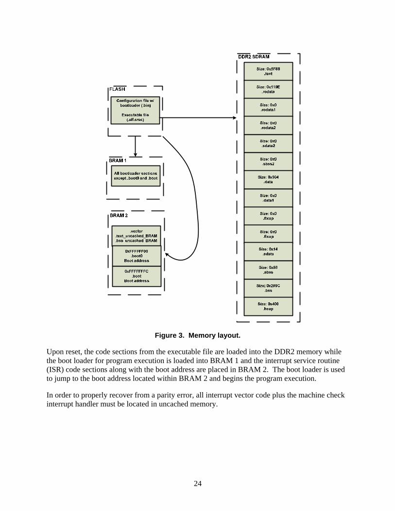
4.1.1 Memory Layout
The memory layout is shown in Figure 3. The configuration file and executable file are stored in linear flash on the ML507 board. Two noncacheable on-chip memory units are used within the FPGA, block RAM 1 (BRAM 1) and BRAM 2, while the cacheable off-chip memory uses the DDR2 synchronous dynamic random-access memory (SDRAM) on the ML507 board.
23
Figure 3. Memory layout.
Upon reset, the code sections from the executable file are loaded into the DDR2 memory while the boot loader for program execution is loaded into BRAM 1 and the interrupt service routine (ISR) code sections along with the boot address are placed in BRAM 2. The boot loader is used to jump to the boot address located within BRAM 2 and begins the program execution.
In order to properly recover from a parity error, all interrupt vector code plus the machine check interrupt handler must be located in uncached memory.
24
4.1.2 Software Testing
Figure 4 represents the flow used in bench testing the cache mitigation scheme.
MACHINE CHECK EXCEPTION
INIT. EXCEPTION HANDLER W/ ISR
ENABLE ALL EXCEPTIONS ENABLE CACHE
BEGIN BENCH TEST
CACHE PARITY ERROR
JUMP TO ISR
DETERMINE PARITY ERROR TYPE
DISABLE CACHE
OUTPUT CACHE LINE INFO
TERMINAL WINDOW
CLEAR DCACHE & ICACHE
ENABLE CACHE
CONTINUE PROGRAM EXEC.
ISR
YES NO
INSERT PARITY ERROR
ALL 9 TESTED? OUTPUT PARITY
ERROR NOT DETECTED
CLEAR CACHE
OUTPUT MENU
SELECT TEST
LOOP/SINGLE TEST
RETURN FROM ISR
SINGLE/LOOP TEST
LOOP
Figure 4. Bench testing flow diagram.
As shown in Figure 4, the software application created first initializes the exception handler with the ISR. The ISR is used to handle the machine check interrupt caused by a parity error within the cache. The ISR performs the necessary actions needed to recover from the parity error as listed in Table 3. Exceptions are then enabled within the processor and both the data and instruction cache are enabled. The program will then begin bench testing by inserting one of the nine parity errors. If a machine check interrupt occurs, the ISR will execute and output invalid cache lines to the terminal window. The ISR will also flush the cache and reenable the cache. Program execution will then continue. This process will continue for each of the nine parity errors. Note that if the machine check interrupt does not occur, the user is notified at the terminal window. Finally, after each of the nine parity errors are tested, a menu is outputted to
25
the user on the terminal window. The user is then given the option to test a single parity error, test all nine parity errors, or test a single parity error nine times.
4.2 Radiation Testing
The cache mitigation scheme was also tested within a heavy ion radiation facility at TAMU in March 2009 and July 2009 to test the validity of the bench testing. The radiation testing conducted in March used a commercial Virtex-5 FPGA and was not mitigated except for the cache. In July the cache mitigation scheme was tested on a radiation-hardened Virtex-5 FPGA and was modified slightly to mitigate some of the issues seen in the March testing.
4.2.1 TAMU Radiation Effects Facility Description
TAMU provides a radiation effects facility, which is where the PPC440 cache parity testing was conducted. Figures 5 and 6 provide a layout of the radiation facility.
Images provided by the TAMU Cyclotron website
Figure 5. TAMU radiation effects facility.
26
Images provided by the TAMU Cyclotron website
Figure 6. Three-dimensional view of radiation facility.
The data room seen in Figures 5 and 6 provides a way to monitor and collect data from the test setup in the lower floor. Two 4-inch-diameter cable passages provide a way to connect the test setup seen on the first floor to the data room located on the second floor.
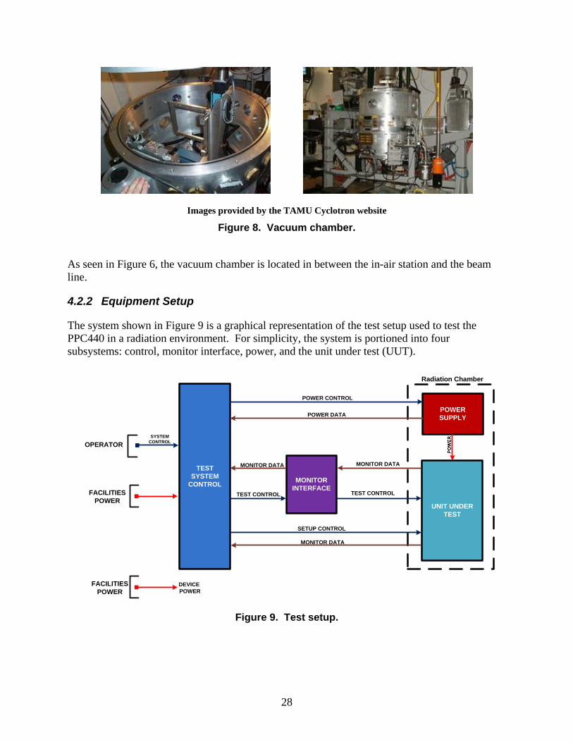
For the March testing the in-air station shown in Figure 7 was used, while the July testing used the vacuum chamber shown in Figure 8.
Images provided by the TAMU Cyclotron website
Figure 7. In-air station.
27
Images provided by the TAMU Cyclotron website
Figure 8. Vacuum chamber.
As seen in Figure 6, the vacuum chamber is located in between the in-air station and the beam line.
4.2.2 Equipment Setup
The system shown in Figure 9 is a graphical representation of the test setup used to test the PPC440 in a radiation environment. For simplicity, the system is portioned into four subsystems: control, monitor interface, power, and the unit under test (UUT).
text
UNIT UNDER TEST
Radiation Chamber
TESTSYSTEM
CONTROL MONITORINTERFACE
POWERSUPPLY
FACILITIES POWER
POWER DATA
MONITOR DATA
POWER CONTROL
TEST CONTROL
MONITOR DATA
TEST CONTROL
SETUP CONTROL
MONITOR DATA
SYSTEM CONTROLOPERATOR
FACILITIES POWER
DEVICEPOWER
Figure 9. Test setup.
28
The test system control unit is used to perform user functionality to the rest of the system. This system controls the triple power supply, monitors the power supply, and can control the UUT before and during testing. Before testing, the test system control is able to set up the UUT for various tests, while monitoring of the UUT is either through the system interface or directly from the UUT. Power to the test system control unit is provided by the facilities.
The monitor interface is used to act as a buffer between the test system control and UUT. Power to the system interface is also provided by the facilities.
The power supply is used to power the UUT and is controlled by the test system control unit. The power supply is located within the radiation chamber.
The UUT is used to test the cache mitigation scheme. Data collected during testing is transferred from the UUT directly to the test system control unit and through the system interface. The UUT is also controlled through the test system controller before testing is started. This allows the UUT to be set up directly from the test system control.
4.2.2.1 Test System Control
The test system control unit is represented in Figure 10 and is used to perform user functionality to the rest of the system. User control is provided by the use of laptops communicating with various parts of the system.
TEST SYSTEM CONTROL
FACILITIES POWER
POWER CONTROLOPERATOR
EVENT DATA
LAPTOP #1
LAPTOP #2
LAPTOP #3
SETUP CONTROL
MONITOR DATA
POWER DATA
POWER CONTROL
CONFIG CONTROLOPERATOR
TEST CONTROLOPERATOR
POWER SUPPLY
MONITOR INTERFACE
UNIT UNDER TEST
SCRUB
CONFIG FPGA
MONITOR DATA
FACILITIES POWER
FACILITIES POWER
DEVICE CONTROL
Figure 10. Test system control.
29
One laptop with a Personal Computer Memory Card International Association (PCMCIA) general purpose instrumentation bus (GPIB) card is used to control the power supplies located within the radiation chamber. This laptop also serves to record voltages and currents for the UUT. Power supplied to this laptop is provided from the facilities.
A second laptop with a PCMCIA digital input/output (I/O) card connects to the system interface through a digital I/O ribbon cable. This laptop is used to control and collect event data from the UUT through the use of a custom graphics user interface (GUI), shown in Figure 11. Event data collected is in the form of counters.
Figure 11. Configuration monitor interface.
The configuration monitor (CONFIGMON) GUI also is used to configure the UUT within the test system. Configuration consists of loading the configuration bit files into the UUT. The CONFIGMON GUI is also used to activate scrubbing within the UUT to ensure that the SEUs within the configuration bit files are reduced during beam testing. During testing the XRTC group monitored and operated the CONFIGMON GUI.
30
Finally, a third laptop with a PCMCIA digital I/O card connects to the system interface through a digital I/O ribbon cable. This laptop is used to control and collect data from the UUT through the use of a custom GUI, shown in Figure 12.
Figure 12. Functional monitor interface.
31
The information collected is in the form of register data or counters from the UUT in the event of a cache parity error. Table 4 describes the features shown in Figure 12. Items not listed in the table were not used during testing.
Tag Name Description Cache Scan Heart Beat Increments each time the UUT sends a pulse. Signifies that
the UUT is operational. Cache Error Count Increments each time a bad cache line is found within an
ICache or DCache line. Cache Data Select – 2-bits Specifies which packet from the UUT has been received, i.e.,
00 – packet 0 has been received. Cache Set – 8 bits The set location of the affected cache line. Cache Type – 1 bit 1 if tag parity error, 0 if data store parity error Cache Way – 8 bits The way location of the affected cache line. Cache ID 1 if Icache parity error, 0 if Dcache Parity error. Cache Tag Contains the tag debug register for either the Icache or
Dcache within the affected cache line. Cache Tag/Register If data store parity error, then contains the affected data
register; otherwise, contains the affected tag register. Cache_tlb_error_count_s Increments each time a TLB parity error is detected. Cache_icache_error_count_s Increments each time a Icache parity error is detected. Cache_dcache_error_count_s Increments each time a Dcache parity error is detected. Cache_dflush_error_count_s Increments each time a Dcache flush parity error is detected. Ck0 On Enables or disables the clock to the PPC440. DUT reset Resets the PPC440. Rate/Heartbeat Enables the output of the heartbeat to ensure the FUNCMON
is working. Logging Used to record information during beam testing.
The third laptop also uses the RS232 to monitor debug information from the PowerPC (PPC). Power is supplied to the laptops through the facility.
32
4.2.2.2 Monitor Interface
The monitor interface of the test system is represented in Figure 13.
Figure 13. System interface.
The monitor interface is used to pass information from the UUT to the test system control unit. This subsystem contains the SEU monitor units, also called “brain boxes”. Data and control is sent to the UUT through 40-pin twisted-pair ribbon cables.
The power to the brain boxes is supplied from the facilities.
4.2.2.3 Unit Under Test
Figure 14 shows the physical layout of the UUT4 used in the test system.
This system contains three FPGAs, two of which are XC2VP70 FPGAs, while the third is either a XC5VFX130T or XC5VFX1 FPGA. The FX1 FPGA is an SEU Immune Reconfigurable FPGA (SIRF). The Virtex-5 FPGA is the device under test (DUT) and is the FPGA that is exposed to the beam in the radiation facility. Both V2P FPGAs are used as the configuration monitor (CONFIGMON) and the functional monitor (FUNCMON). The CONFIGMON FPGA is used to configure both the FUNCMON FPGA and the DUT FPGA. The FUNCMON FPGA is used to monitor the DUT, act as external memory to the DUT, and provide control to the DUT.
4 Motherboard designed by SEAKR Engineering, Inc.
33
Figure 14. Unit under test physical layout.
34
4.2.3 Cache Mitigation Design Modifications
In order to adequately test the cache mitigation scheme, the processor needed to be isolated as much as possible. Since the surrounding fabric around the processor is highly susceptible to SEUs, trying to mitigate as much of it as possible helps to ensure a better test of the cache mitigation scheme.
Figure 15 represents a simplified version of the DUT used during testing.
Figure 15. Device under test.
Figure 15 shows how the processor is isolated within the FPGA for testing. As seen in Figure 15, there are still some resources that the PPC440 uses within the FPGA, such as the processor local bus (PLB) and memory controllers.
35
The general flow of the cache mitigation scheme is shown in Figure 16.
Figure 16. Cache mitigation flow diagram.
Figure 16 shows how the PPC440 executes during testing. Upon receiving a parity error within the cache due to an SEU, the processor immediately throws a machine check interrupt, causing the ISR to handle the interrupt and recover from the parity error. Upon recovery the processor resumes execution. Note that for the March 2009 testing there was no pattern selection for filling the data cache.
The following sections discuss additions or changes to the design in order to test the cache mitigation scheme.
36
4.2.3.1 Radiation-Hardened By Design
In order to reduce the number of SEUs within the soft logic of the FPGA, a radiation-hardened by design FPGA, SIRF, was used during testing. As seen in Figure 15, the PPC440 is embedded into the SIRF part. The SIRF part was used during the July 2009 testing while a commercial Virtex-5 was used during the March 2009 testing.
4.2.3.2 Soft Intellectual Property
The use of soft intellectual property (IP) is also a problem during radiation testing since the IP uses the configurable logic of the FPGA. This presents another target to radiation that can cause SEUs within the system. To avoid this, removal or simplification of the IP can help reduce the number of SEUs.
One such IP that was removed was the clock generator used within the Embedded Development Kit. This IP was replaced with a generic clock generator, as shown in Figure 15, to reduce the target size of the IP. The generic clock IP was used for both the March 2009 testing and the July 2009 testing.
As mentioned previously, the processor still uses IP that cannot be removed such as the PLB, or is necessary to support testing, such as the memory controllers.
4.2.3.3 Block RAM
Block RAM is another large target when exposed to radiation and an SEU within BRAM can cause the processor to become unresponsive. In order to avoid using BRAM within the DUT FPGA, the code was initialized in two FUNCMON BRAMs. One BRAM would store the code necessary to execute the cache mitigation scheme for the processor while the second BRAM was used to store the interrupt-handling routine used to recover from cache parity errors. This implementation is shown in Figure 15. This design change was implemented during the March 2009 testing.
Since BRAM was no longer used within the DUT, FUNCMON could be initialized with the code, which avoided using the Xilinx Microprocessor Debugger (XMD). Though XMD was not used during testing, this ensured that XMD would not cause any problems during testing. This feature was designed after the March 2009 testing and was used at the July 2009 testing. During the March 2009 testing XMD was used to initialize FUNCMON with the code.
4.2.3.4 Data Cache
In order to adequately test the cache mitigation scheme, the data cache was filled with either all ones or zeros. This was used to ensure that data was being placed into the cache and to ensure that an SEU would cause not only instruction cache errors, but data cache errors as well. Filling the data cache is implemented after an iteration of the Dhrystone application runs, as shown in Figure 16. This software addition was implemented for the July 2009 testing.
37
4.2.4 Radiation Test Results
The following sections present the results of both the March 2009 test and the July 2009 test. Following the results of both the March 2009 testing and the July 2009 testing is a comparison of the two tests. This is only used as a general comparison and is in no way a definite comparison since there is not enough test data for both the March 2009 test and the July 2009 test.
4.2.4.1 Commercial Test Results
The March 2009 test was an unmitigated design except for the changes described in the previous sections. Two tests were conducted on the commercial FX130T, a dynamic test and a static test. The results presented show cases in which the processor became unresponsive. These cases may not have been associated with the cache, but could have been due to other unmitigated areas. Also note that for both tests, the DUT was being scrubbed during testing to reduce the number of SEUs within the configuration of the FPGA. 4.2.4.1.1 Dynamic Testing
Dynamic testing was the first test conducted during the beam testing. For this test the DUT was configured with internal BRAM. The internal BRAM was used as uncached memory while the FUNCMON’s BRAM was used as external cached memory. This test was mostly designed to give the PPC440 a “taste” of the beam. In other words, since the design was fairly unmitigated except for the cache, the probability of the PPC440 failing was pretty high. Therefore the PPC440 was only exposed to small amounts of radiation during this test. During testing, the DUT was scrubbed through CONFIGMON to reduce the number of upsets in the configuration bitstream. The dynamic testing consisted of the PPC440 running a continuous loop of the Dhrystone application. Iterations of the Dhryloop took approximately 1.31 seconds and counted as a single test. The typical output seen in the terminal window is shown in
Figure 17
stone
. --BEAM MODE --Test #: 2 Dhrystone Benchmark, Version 2.1 (Language: C) Program compiled without 'register' attribute Execution starting: 100000 runs through Dhrystone Execution finished; Execution Count: 81000065 Begin 1 Stop 81000066 Test Execution Time: 1.31000065 seconds Dhrystones per second: 100000 watchdog status register: 0x00000000
Figure 17. Commercial testing terminal debug.
38
If a parity error was detected in the PPC440, then the terminal window would output the following debug information as sh
Figure 18. own in
--BEAM MODE --Test #: 20 Dhrystone Benchmark, Version 2.1 (Language: C) Program compiled without 'register' attribute Execution starting: 100000 runs through Dhrystone cache data parity: 0x00000001 line: 53, word: 6, set: 8, way: 3 data register: 0x5FE3FB78 tag high: 0x00001CB0 tag low: 0x00000100 Packet 0: Sent 20608 Packet 1: Sent 1CB0 Packet 2: Sent 5FE3FB78 Execution finished; Execution Count: 94741608 Begin 1 Stop 94741609 Test Execution Time: 1.44741608 seconds Dhrystones per second: 100000 watchdog status register: 0x00000000
Figure 18. Commercial parity detection and recovery debug.
Note that the data shown in the output window is also transmitted to the FUNCMON GUI, as shown in Figure 12. For example, f
Figure 18, an instruction cache parity error is detected within the hardware of the PPC. The PPCissues a machine check interrupt causing the ISR to execute. The ISR clears both the instructionand data cache, increments a counter for the specific parity error detected, and sends this information to the GUI and the terminal window. The ISR then returns from the interrupt and the processor continues execution.
rom
4.2.4.1.1.1 Dynamic Testing Results5 Table 5 summarizes the type of radiation used during the nine runs of dynamic testing. Each run used the same heavy ion at the same energy, therefore the particle range and the linear energy transfer (LET) was also the same for each run. The LET is the measure of energy deposition in a material and has units of MeV-cm2/mg. Also, the testing was conducted at an angle normal to the surface, zero angle.
5 Radiation data recorded by Jet Propulsion Laboratory/Xilink Radiation Test Consortium at the beam testing site.
39
Table 6 shows the length of time that the part was exposed to the beam along with the heavy ion beam flux, total fluence for the run, and the resulting ionizing dose deposited in the device. Each run consisted of a different setting as listed in the table.
Average 1.96E+01 1.06E+03 2.17E+04 1.52E+00 The run time for the commercial testing is shown in Figure 19.
Figure 19. Commercial execution time.
The run time in Figure 19 shows how long the processor executed while exposed to the beam before becoming unresponsive. The processor was unable to run longer than a minute.
40
Figure 20 shows the number of instruction cache and data cache parity errors that were detected and recovered from, while Figure 21 shows the total number of parity errors detected within a cache line.
For example, looking at Figures 20 and 21, test 8 illustrates that there were four instruction cache parity errors and two data cache parity errors for a total of 6 parity errors. For the six parity errors, there were a total of 42 cache line errors.
41
Overall, the commercial test performed poorly and was never able to run for a long period of time due to the unmitigated design.
4.2.4.1.2 Static Testing
Static testing was used to try and get a better test of the cache mitigation scheme since the design was not fully mitigated. This test would reduce the number of unknowns affecting the design during beam testing. The static test consisted of the following steps:
• Start the PPC440 and allow the Dhrystone application to begin.
• Before starting the beam, stop the clock on the PPC440. This was done through the FUNCMON GUI.
• Start the beam for a set amount of time.
• Stop the beam and scrub the DUT through CONFIGMON.
• Start the clock on the PPC440 again resuming execution of the processor.
• Monitor the debug output on the terminal window and FUNCMON GUI to see if there is a cache parity error and if the system recovers from that parity error.
The only design modification that was used during this testing was the BRAM modification discussed in the previous section.
4.2.4.1.2.1 Static Testing Results6 Table 7 summarizes the type of radiation used during static testing. Each run used the same heavy ion at the same energy, therefore the particle range and the linear energy transfer (LET) was also the same for each run. The LET is the measure of energy deposition in a material and has units of MeV-cm2/mg. The testing was also conducted at an angle normal to the surface, zero angle.
6 Radiation data recorded by Jet Propulsion Laboratory/Xilink Radiation Test Consortium at the beam testing site.
42
Table 8 shows the length of time that the part was exposed to the beam along with the heavy ion beam flux, total fluence for the run, and the resulting ionizing dose deposited in the device. Each run consisted of a different setting as listed in the table. Run 553 has no radiation information recorded due to human error.
The results for the static testing are inconclusive since there were discrepancies found between the GUI logs and the terminal debug logs. Also, the PPC440 became unresponsive on most of the runs after restarting the clock.
4.2.4.2 Radiation Hardened Test Results
Testing the cache mitigation scheme in the SIRF PPC440 consisted of only one test, a dynamic test. As stated previously, testing was conducted on the FX1 SIRF within the vacuum chamber. The DUT was irradiated until the processor stopped responding due to a SEFI. Upon receiving a SEFI the processor was unable to be reset from an external reset. The results of this test are described in the following section.
4.2.4.2.1 Dynamic Testing
Dynamic testing was the only cache mitigation test conducted due to beam testing time constraints. During testing, the DUT was scrubbed through CONFIGMON to reduce the number of upsets in the configuration bitstream.
43
The dynamic testing consisted of the PPC440 running a continuous loop of the Dhrystone application and filling the data cache with either all ones or zeros depending on the user’s input to the FUNCMON GUI. Iterations of the Dhrystone loop took approximately 3.089 seconds and counted as a single test. The typical output seen in the terminal window is shown in Figure 22. Note that the output was modified from the March 2009 testing to provide more information. Also, as stated previously, the July 2009 test also added the feature of filling the data cache with either ones or zeros.
--BEAM MODE --Test #: 5
Pattern selection - 1:
Dhrystone Benchmark, Version 2.1 (Language: C)
Program compiled without 'register' attribute
Execution starting: 100000 runs through Dhrystone
Execution finished; Execution Count: 158900074
Begin 1
Stop 158900075
Test Execution Time: 3.08900074 seconds
Dhrystones per second: 33333
Begin filling cache with pattern 0xFFFFFFFF
watchdog status register: 0x00000000
Figure 22. SIRF Terminal debug.
44
If a parity error was detected in the PPC440, then the terminal window would output the debug information, as shown in Figure 23.
--BEAM MODE --Test #: 21
Pattern selection - 1:
Dhrystone Benchmark, Version 2.1 (Language: C)
Program compiled without 'register' attribute
Execution starting: 100000 runs through Dhrystone
Execution finished; Execution Count: 175841963
Begin 1
Stop 175841964
Test Execution Time: 3.25841963 seconds
Dhrystones per second: 33333
Begin filling cache with pattern 0xFFFFFFFF
GOT ICache Parity Error!
-- Current Cache Parity Error Count:
INSTRUCTION PLB ERROR: 0
PLB DATA READ ERROR: 0
PLB DATA WRITE ERROR: 0
TLB PARITY ERROR: 0
INSTRUCTION CACHE PARITY ERROR: 1
DATA CACHE PARITY ERROR: 0
DATA CACHE FLUSH PARITY ERROR: 0
watchdog status register: 0x00000000
Figure 23. SIRF Parity detection and recovery debug.
The same output data is also transmitted to the FUNCMON GUI.
45
4.2.4.2.1.1 SIRF Results7 Table 9 summarizes the type of radiation used during each run of dynamic testing. Each run used the same heavy ion at the same energy, therefore the particle range and the linear energy transfer (LET) was also the same for each run. The LET is the measure of energy deposition in a material and has units of MeV-cm2/mg. The run number listed is the corresponding order that the scheme was tested.
Table 9. SIRF Dynamic Testing Radiation Type.
Run # Test Energy (Mev/u)
Energy (MeV) Ion LET Eff
Range Degrader
30 Ones pattern upsets
15 2955 Au 90.1 79.9 none
31 Ones pattern upsets
15 2955 Au 90.1 79.9 none
32 Ones pattern upsets
15 2955 Au 90.1 79.9 none
33 Zeros pattern upsets
15 2955 Au 90.1 79.9 none
34 Zeros pattern upsets
15 2955 Au 90.1 79.9 none
35 Zeros pattern upsets
15 2955 Au 90.1 79.9 none
36 Zeros pattern upsets
15 2955 Au 90.1 79.9 none
Table 10 shows the length of time that the part was exposed to the beam along with the heavy ion beam flux, total fluence for the run, and the resulting ionizing dose deposited in the device. Each run consisted of a different setting as listed in the table.
7 Radiation data recorded by Jet Propulsion Laboratory/Xilink Radiation Test Consortium at the beam testing site.
46
Figure 24 graphs the run time for each test.
Figure 24. SIRF execution time.
As mentioned previously, for each test the DUT was irradiated until the processor stopped responding. The run times listed in Table 10 and shown in Figure 24 show that the longest run time was 258.15 seconds while the data cache was being filled with ones. The average run time for the seven tests was 109.3 seconds.
Figure 25 shows the number of instruction cache and data cache parity errors that were detected and recovered from, while Figure 26 shows the total number of parity errors detected within a cache line.
From Figure 27, the cross-section or size of the target node for the cache per byte line ranged from 9.77E-6 cm2/cache line to 1.12E-5 cm2/cache line, with an average cross-section of 8.01E-6 cm2/cache line.
Figure 27 also shows the cross section for the number of PPC crashes observed. As mentioned previously, each test ran until the processor became unresponsive (crashed). Thus, the cross section for this case is nothing more than 1/fluence and is much higher than the cache line errors. From Figure 27, the average PPC crash was 8.65E-5 cm2/cache line. In order to get an adequate cross-section vs. LET curve more test data is required along with a wider LET spectrum.
48
4.2.4.3 Virtex-5 Test Comparison
The following section compares both the dynamic testing of the March 2009 beam test to the dynamic testing of the July 2009 beam test. As mentioned previously, this is a general comparison since both tests were conducted under different parameters.
Table 11 shows a comparison of the test parameters used in testing the SIRF device and the commercial device. The main difference is the LET at which the devices were tested. Future testing will cover more LET values which should allow for a more direct comparison of upset cross sections.
Table 11. Comparison of Parameters from SIRF Test and Commercial Virtex-5 Test.
SIRF Test Parameters Commercial Virtex-5 Test Parameters
Avg. Flux (cm-2 s-1) 1.07E+02 1.06E+03 Avg. Fluence (cm-2) 1.16E+04 2.17E+04 Avg. Dose (rad(Si)) 1.67E+01 1.52E+00 Energy (MeV) 2955 135 LET (MeV-cm2/mg) 91 4.3 Effective Range (μm) 79.9 93.8 Test Platform Vacuum Chamber In-Air Station Ion Type Gold Neon Avg. Run Time (s) 1.09E+02 1.96E+01
Figure 28 shows a comparison of the Virtex-5 commercial testing conducted in March 2009 and the SIRF testing conducted in July 2009.
Figure 28. SIRF execution time vs. Virtex-5 commercial execution time.
49
Figure 28 shows that the commercial Virtex-5 test performed at a much lower execution time than the SIRF device which is expected since the design is not mitigated except for the cache. The longest run time recorded was test 8, which ran for only 56.6 seconds.
Figures 29 and 30 show a comparison of the unmitigated design to the SIRF design in parity detection/recovery and total cache line upsets.
Figure 29. SIRF vs. commercial Virtex-5 parity detection/recovery.
Figure 30. SIRF cache line errors vs. commercial Virtex-5 cache line errors.
Though the unmitigated design shows fewer errors detected, note that the run time for the unmitigated design was much lower due to PPC failures (Figure 28).
50
5. CONCLUSION
Both the bench testing and radiation testing showed that the cache mitigation scheme is a viable solution when attempting to mitigate the embedded hard-core processor from SEUs. As mentioned earlier, these comparisons are general since the parameters used during testing were different, especially with the LET used. That is, the SIRF part was exposed to a much higher LET than the commercial part. A larger LET deposits more charge onto the FPGA and the more charge there is the more likely it is to cause an upset. Overall, there are still some challenges that need to be investigated to adequately test the cache mitigation scheme.
One of these challenges is determining what is causing the processor to become unresponsive. This is difficult because the processor is a large black box with no visible way to determine what could be causing the processor to become unresponsive (i.e., is the cache getting hit or is something else within the processor getting hit?). For example, the general and special purpose registers or the TLB could be getting hit during the radiation testing, causing the processor to lockup. Proper mitigation of the processor should allow for longer run times and a way to isolate the cache mitigation scheme during testing.
Another issue during testing is that the processor is still using some soft IP such as the PLB, memory controllers, and processor JTAG. Though these should be mitigated within the radiation-hardened FPGA, additional mitigation schemes might be necessary to provide a more robust system to isolate the cache for testing.
An interesting result from the cache mitigation testing was the inability to reset the processor upon receiving a SEFI. Both the SIRF and commercial Virtex-5 were unable to recover upon receiving an external reset.
In order to adequately test the cache mitigation scheme more and longer run times are needed. The cache mitigation scheme was tested only for seven and nine runs respectively with only one LET used. More data results are needed to gain a better analysis of the cache mitigation scheme.
Finally, as this study transitions from embedded hard-core processors to soft-core processors, further mitigation studies into reducing the number of SEUs within the cache will need to be considered.
51
52
53
DISTRIBUTION
1 MS0503 James W. Daniels 5337 1 MS0503 Dominic A. Perea 5337 1 MS0503 Mythi M. To 5337 1 MS0503 Donald E. Tolsch 5339 1 MS0513 Glen I. Magee 5336 1 MS0513 Richard D. Hunt 5336 1 MS0521 Ed E. Boucheron 2617 1 MS0661 Daniel E. Gallegos 2623 1 MS0661 Mark W. Learn 2623 1 MS0661 Aaron D. Niese 2623 1 MS0672 Brian P. Van Leeuwen 5628 1 MS0964 Brian C. Brock 5735 1 MS0966 Jae W. Lee 5733 1 MS0971 Ethan L. Blansett 5735 1 MS0972 Kurt R. Lanes 5550 1 MS0980 J. Doug Clark 5732 1 MS0980 Jay F. Jakubczak 5710 1 MS0980 Matt P. Napier 5571 1 MS0980 Toby O. Townsend 5717 1 MS0982 Dan J. Kral 5732 1 MS0986 David M. Bullington 2664 1 MS0986 Jonathon W. Donaldson 2664 1 MS0986 David Heine 2664 1 MS0986 Jeffrey L. Kalb 2664 1 MS0986 David S. Lee 2664 1 MS0986 J. (Heidi) Ruffner 2664 1 MS1235 John M. Eldridge 5632 1 MS1243 Raymond H. Byrne 5535 1 MS0123 D. Chavez, LDRD Office 1011 1 MS0899 Technical Library 9536 (electronic copy)