Modeling and Analysis of Defective Ground Plane Microstrip Structures Evi Van Nechel Academic year 2013-2014 Master thesis submitted under the supervision of Prof. dr. ir. Yves Rolain Prof. dr. ir. Gerd Vandersteen The co-supervision of ir. Matthias Caenepeel In order to be awarded the Master’s Degree in Electronics and Information Technology Engineering
Transcript
Modeling and Analysis of DefectiveGround Plane Microstrip Structures
Evi Van Nechel
Academic year2013-2014
Master thesis submitted under the supervision ofProf. dr. ir. Yves RolainProf. dr. ir. Gerd Vandersteen
The co-supervision ofir. Matthias Caenepeel
In order to be awarded the Master’s Degree inElectronics and Information Technology Engineering
Acknowledgements
First of all I would like to thank my promoter Yves for giving me the best guidance during the course
of the thesis and for the condence he has put in me. I also want to thank my adviser Matthias
for all his good advice and support and for the motivation he gave me. Next, I would like to thank
Gerd for exploring the edges of the EM-simulator with me and for coming up with new possibilities
every time. Furthermore, I want to thank the whole ELEC-department for creating a nice and
comfortable environment with special thanks to Johan Pattyn for always carefully fabricating my
PCB-designs and to Maral for taking my mind of the thesis when needed and who always kept me
motivated.
Very special thanks goes to my boyfriend Kenny for his support, his love and his enormous amount
of patience. I want to thank all my classmates, especially Piet and Steluta, for the joyful moments
and the memorable quotes of the week. I also want to thank Glenn and Glenn for the relaxing lunch
times during the year. And last but not least, I want to thank my family and friends for their care
and understanding.
Abstract
Title - Modeling and analysis of defective ground plane microstrip structures
Author - Evi Van Nechel
Master's degree - Electronics and Information Technology Engineering
Academic year - 2013-2014
Abstract - Coupled line lters are widely used in modern microwave communication systems.
The classical parallel-coupled transmission-line-resonator lter developed by Cohn [1] has two main
shortcomings when designed in microstrip technology: 1) the presence of spurious passbands at the
harmonic responses; 2) the diculty to design wideband lters. When the classical approach fails,
alternative solutions are needed. In this work, we investigate whether introducing slots in the ground
plane can result in wideband lters with a low insertion loss. The aim of this thesis is to examine
the eect of resonant apertures in the ground plane of microstrip structures and to investigate their
potential benets in lter design.
The work consists of ve main results:
The EM-simulator is shown to be capable of simulating a slotted ground plane accurately.
This is proven with actual designs and measurements.
A simple microstrip line with multiple slots is examined. It is shown that this structure acts as
a bandstop lter. Adding this structure to classical parallel-coupled line lters can attenuate
the harmonic responses, hereby solving the rst drawback.
A lumped-element equivalent circuit model is generated to predict the behavior of the slots.
The novelty in the proposed model is twofold: 1) it predicts anti-resonances and quality factor
accurately; 2) it is symmetric.
A MIMO-LTI-model-based comparison between the EM-simulations and the lumped circuit
model shows that the frequencies of the poles and zeros is accurately predicted, while the
quality factor needs some additional improvement.
A nal analysis of a simple coupled line structure with a slotted ground plane shows that
introducing slots in the ground plane indeed increases the coupling. This can be used to solve
the second drawback of the classical approach. Further research is needed to include this
Coupled line lters are widely used in modern microwave communication systems. The classical and
widely used parallel-coupled transmission-line-resonator lter design method developed by Cohn [1]
has proven to be successful, but it has two main shortcomings when a design in microstrip technology
is aimed at: 1) spurious passbands are present at the harmonic response; 2) wideband lters (>
30 % [1]) are very hard to obtain.
Wideband lters require a strong coupling between the coupled lines. To achieve this strong coupling
in a classical coupled line, the gap between the lines needs to decrease accordingly. However,
decreasing the dimensions of the gap is not always possible since, at some point, mechanical tolerance
induces that the structure cannot be fabricated accurately anymore.
When the classical approach fails, alternative solutions are needed. In this work, we investigate
whether introducing slots in the ground plane can result in wideband lters with a low insertion
loss. The aim of this thesis is to examine the eect of resonant apertures in the ground plane of
microstrip structures and to investigate their potential benets for an application in lter design.
Chapter 2 veries whether the used EM-simulator [2] is capable of simulating a slotted ground
plane accurately and determines this accuracy. We give an overview of the dierent settings of the
EM-simulator that inuence the accuracy and based on this a set of valid settings is obtained to
simulate a nite ground plane structure. The choice of the settings is veried using an actual design
and its realization as we compare the simulated to the measured S-parameters.
Chapter 3 examines the eect of rectangular slots in the ground plane on the frequency response
of a single transmission line. A lumped-element equivalent circuit model is proposed and validated
using an example that is realized and measured again. Since the original lumped model taken from
the literature is not complex enough to yield an accurate model, Section 3.5 proposes improvements
to the the lumped circuit model: symmetry is hereby imposed and the circuit model can predict
anti-resonances and quality factor more accurately.
1
2 CHAPTER 1. INTRODUCTION
Obtaining a model that can predict the eects of slotted ground plane structures accurately is a
very important step towards a proper design procedure. In Section 3.6 we discuss a parametric
MIMO-model to verify how good the improved model actually is. Can it predict the behavior of
the transmission line structure suciently well? This comparison is based on the comparison of the
position of the poles and zeros of the model.
Next we examine a simple coupled line structure with a defective ground plane in Chapter 4. We
verify whether the extra complication of the line coupling, next to the slot coupling, still leads to
accurate and correct simulation results. Three dierent coupled line structures of increasing com-
plexity are selected to gradually work from a coupled line to a complete defective ground lineset.
The dierent steps are again validated with measurements. The structures are physically realized
and measured with the Vector Network Analyzer. The eect of the coupling of two lines in combi-
nation with slots in the ground plane is assumed and analyzed and the benets for the use in lter
design are discussed.
Finally, some conclusions are drawn about the research on defective ground plane microstrip struc-
tures and their potential use in lter design. We also briey touch the future perspectives on this
subject.
Chapter 2
Simulator settings
2.1 Introduction
The goal of this thesis is to examine the eect of apertures in the ground plane of microstrip
structures. Hence, it is very important to be able to properly simulate these eects since the rst
stage of every design is based on simulations. We want these simulations to be as close as possible to
the actual measured results and therefore, the settings of the used simulator should be chosen with
care. Since simulating in a correct way is very important, this chapter is devoted to the choice of
the simulator settings and its inuences. In this case, the Momentum simulator [2] of the Advanced
Design System (ADS) [3] software of Agilent is used.
Section 2.2 gives an overview of the dierent possible settings of the Momentum simulator. The
inuence of the dierent settings is discussed based on an example. As an example, a coupled line
lter is used (Section 2.4). The eect of the introduction of a nite ground plane on this lters'
response is examined and compared to the simulation with innite ground plane. The design is
realized in hardware and the measurements are compared to the simulations.
2.2 Momentum setup
This section outlines the dierent settings of the Momentum setup. The pros and cons of some
important settings are discussed. This is necessary to justify the choice of the settings for the
considered application.
2.2.1 Simulation mode
Momentum has two simulation modes, the microwave mode and the radio frequency (RF) mode.
The main dierence between them is the way the Greens' functions are calculated.
3
4 CHAPTER 2. SIMULATOR SETTINGS
The microwave or full-wave mode uses full-wave Greens' functions, which are frequency dependent
and fully characterize the substrate. In the RF or quasi-static mode, however, the Greens' functions
are frequency independent and hence, some simplications to the Maxwell equations are made. This
results in real and frequency independent inductances and capacitances, compared to complex and
frequency dependent element values in case of the full-wave Greens' functions. Furthermore the
RF mode does not incorporate the high frequency losses in the ground plane, unlike the microwave
mode.
Thus, the microwave mode uses less approximations and the results are more accurate when selecting
this mode. The downside of using the microwave mode is that the simulation time is much longer
than in case of the RF mode. [4]
2.2.2 Mesh settings
It is impossible for the simulator to calculate the voltage and current distributions at every single
point of a transmission line. Therefore, some points need to be specied at which the calculations
are done. Hence, the transmission lines are divided in small cells. The mesh is the collection of
these cells. At the crossings of the cells, the necessary functions are calculated.
There are several settings related to the mesh that are very important. The mesh frequency is
the frequency that determines the wavelength that is used for the mesh density. Two options are
possible here. We can use the default value, which sets the mesh frequency to the highest simulation
frequency. This ensures that the simulation results are accurate over the whole range of simulated
frequencies. The other option is that the user denes the mesh frequency himself.
The mesh density determines the number of cells per wavelength. This wavelength is calculated
from the mesh frequency and the relative permittivity. On the one hand the mesh needs to be dense
enough in order to capture real world spatial variations of the current/voltage distribution. A rule
of thumb is to use 20 cells per wavelength. A denser mesh can be obtained by increasing either the
mesh frequency or the number of cells per wavelength. The downside of making the mesh denser
is that it increases the simulation time. On the other hand, making the mesh too dense can even
result in wrong solutions due to numerical inaccuracy.
To overcome problems in the neighborhood of the edge of a structure, an edge mesh can be used.
This results in a higher accuracy for the simulations, but again this comes at the cost of an increased
simulation time.
Furthermore, the mesh reduction can be disabled. The mesh reduction is a tool that removes
possible redundancies and thus lowers the complexity of the mesh. Disabling the mesh reduction
results in a higher accuracy as well. The drawback is that the rules used to prune the mesh are not
clear and not parametrized. [5]
2.2. MOMENTUM SETUP 5
2.2.3 Frequency plan
An important setting here is the type of the frequency plan, which can be chosen to be 'linear'
or 'adaptive'. For both types the start and stop frequency needs to be specied. When a linear
frequency plan is used, the frequencies to be simulated are chosen to be equidistant. The distance
is set by the user by specifying either the number of points or the frequency step. The user has full
control over the exact simulation frequencies.
This is not the case if an adaptive frequency plan is used. The frequencies are chosen by the simulator
itself. The rule is to use a larger density in the frequency bands where the scattering parameters
(S-parameters) vary more. If the simulator notices large variations of the S-parameters, the number
of frequency points will be increased in that region and decreased in zones where nothing happens.
Hence, the user has no control anymore over the exact frequencies. Only the maximum number of
frequency points can be specied in this case.
2.2.4 Substrate denition
There are two types of substrate denitions that are used for the remainder of the text: an innite
substrate and a nite one.
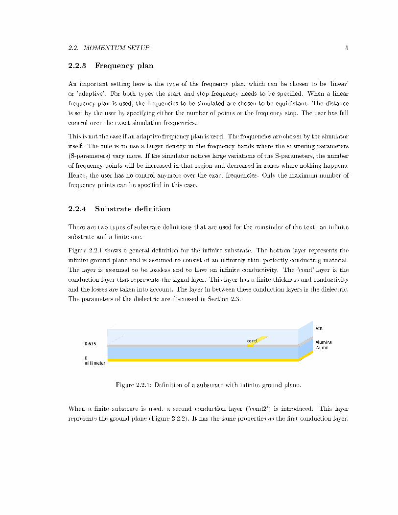
Figure 2.2.1 shows a general denition for the innite substrate. The bottom layer represents the
innite ground plane and is assumed to consist of an innitely thin, perfectly conducting material.
The layer is assumed to be lossless and to have an innite conductivity. The 'cond'-layer is the
conduction layer that represents the signal layer. This layer has a nite thickness and conductivity
and the losses are taken into account. The layer in between these conduction layers is the dielectric.
The parameters of the dielectric are discussed in Section 2.3.
Figure 2.2.1: Denition of a substrate with innite ground plane.
When a nite substrate is used, a second conduction layer ('cond2') is introduced. This layer
represents the ground plane (Figure 2.2.2). It has the same properties as the rst conduction layer.
6 CHAPTER 2. SIMULATOR SETTINGS
Figure 2.2.2: Denition of a substrate with nite ground plane.
2.2.5 Dening ports to interact with the design
A port consists of two terminals, a negative and a positive one. The positive terminal is situated at
the signal layer, the negative terminal at the ground layer.
In case of an innite substrate, the ports are dened as shown in Figure 2.2.3. Here, pins P1 and
P2 are the positive terminals. The negative terminals are implicitly located in the innite ground
plane, as close to the positive terminal as possible.
Figure 2.2.3: Port denitions for a substrate with innite ground plane.
For a nite substrate, the ports are dened as shown in Figure 2.2.4. In this case, the negative
terminals need to be dened explicitly. Pins P3 and P4 are dened as the negative terminals. They
are located at the same position as the positive terminals, P1 and P2.
Figure 2.2.4: Port denitions for a substrate with nite ground plane.
2.3. SUBSTRATE 7
An important setting here is the calibration type. There are a few possibilities, but only two are
applicable in our case, namely a TML-calibration (transmission line calibration) or no calibration.
If a TML-calibration is selected, Momentum automatically adds a transmission line feed line to the
port [6]. If 'None' is selected as calibration type, no calibration is performed.
2.3 Substrate
There are a number of substrate parameters that need to be set. The parameters that are needed
for the conduction layers are the conductance and the thickness of the conduction layer. This was
already mentioned in Section 2.2.4. The parameters of the dielectric are the relative permittivity,
the relative permeability and the dielectric loss model.
The relative permittivity of the dielectric, εr(f), is a complex function of the frequency and can be
written as
εr(f) = ε′(f)(1− j.tanδ(f)) (2.3.1)
with ε′(f) the real part of εr(f) and δ(f) the angle between the real and the imaginary part. The
imaginary part represents the substrate losses.
The relative permeability of the dielectric, µr(f), is also a complex function of the frequency. The
relative permeability of the materials used as a substrate in microwave applications is very near
unity and the conductivity of the dielectric is very low. Hence, we can set the real part of the
relative permeability to 1 and the imaginary part to 0.
There are four parameters for the dielectric loss model, namely the model type, the frequency at
which εr has been measured (fM ) and the lower and upper bound frequency for the model (fL
and fH respectively). There are two possible model types: the frequency independent model or the
Svensson/Djordjevic model.
The frequency independent model assumes that the relative permittivity, εr, is frequency inde-
pendent. The Svensson/Djordjevic model takes the frequency dependency of the permittivity into
account as follows:
εr(f) = ε∞ + a.lnfH + j.f
fL + j.f(2.3.2)
where ε∞ is the value of the permittivity when the frequency approaches innity and a is a constant.
These two parameters are calculated from the substrate parameters ε′, tanδ, fM , fL and fH . fM
is the frequency at which Equations (2.3.1) and (2.3.2) are equivalent for a certain, constant ε′ and
tanδ.
Thus, both models require the user to specify constant values for ε′ and tanδ. When the rst model
is selected, these constant values are used over the whole frequency range. In case of the second
8 CHAPTER 2. SIMULATOR SETTINGS
model, they are used to calculate the parameters ε∞ and a that are needed for the calculation of
ε′(f) and tanδ(f) at the dierent frequencies.
A third option is possible, however. The user can enter frequency dependent expressions for ε′(f)
and tanδ(f). In that case, ADS [3] automatically turns o the Svensson/Djordjevic model. [7]
The substrate that is used in all future designs is a Rogers RO4003 [8] with a thickness of 60 mils.
The conducting material is copper with a conductance of 5.8e7 Sm . The thickness of the conduction
layer is 35µm. The real part of the relative permittivity and the loss tangent parameter are εr = 3.55
and tanδ = 0.0021 at a frequency of fM = 2.5 GHz. The Svensson/Djordjevic model is selected.
2.4 Example: coupled line lter
The example for which the dierent Momentum settings are discussed is a coupled line lter of order
three with a center frequency of 2 GHz. Figure 2.4.1 shows the circuit schematically. The lter is
simulated with an innite and a nite ground plane. The simulator settings as well as the results
are compared. Finally, the simulations are compared to real measurements.
Figure 2.4.1: Schematic of a coupled line lter of order 3 and with a center frequency of 2 GHz.
The layout of the lter with an innite ground plane is shown in Figure 2.4.2. When simulating the
same lter with a nite ground plane, the ground plane needs to be drawn explicitly at a second
conduction layer, 'cond2' (yellow surface in Figure 2.4.3).
2.4. EXAMPLE: COUPLED LINE FILTER 9
Figure 2.4.2: Layout of the coupled line lter with an innite ground plane.
Figure 2.4.3: Layout of the coupled line lter with nite ground plane.
2.4.1 Momentum setup
As mentioned in Section 2.2, there are some dierences in the settings of the substrate and the
port denition depending on the type of the ground plane (nite or innite). In both cases, the
simulation mode, the frequency plan and the mesh settings are kept constant.
2.4.1.1 Simulation mode
It is our intention to replace the innite ground plane by a nite one in order to be able to simulate
apertures in the ground plane. Since the simulation results must be as close to the actually measured
results as possible, we want the simulator to make as few approximations as possible. Therefore,
the microwave mode is preferred above the RF mode.
2.4.1.2 Mesh settings
The mesh frequency is set to be the highest simulation frequency. This ensures that the simulation
results are accurate over the whole range of simulated frequencies. The mesh density is set to 20
cells per wavelength. More accurate simulations could be obtained if the mesh density would be
set to a larger number of cells per wavelength but this increases the simulation time too much once
the nite ground plane is introduced. Furthermore, an edge mesh is used and the mesh reduction
is disabled. In order to properly compare the dierent simulations, the mesh settings are xed to
be the same for all future simulations.
evi.vannechel
Highlight
evi.vannechel
Highlight
evi.vannechel
Highlight
evi.vannechel
Highlight
evi.vannechel
Highlight
10 CHAPTER 2. SIMULATOR SETTINGS
2.4.1.3 Frequency plan
There exists a maximum frequency of operation that is related to the thickness of the substrate.
This is explained as follows. When the frequency is increased, the wavelength decreases. At a certain
point, the wavelength comes very close to the thickness of the substrate and the substrate becomes
non-operational. Besides this, we also know that the simulation time increases very rapidly if the
highest simulation frequency increases. For those reasons, we will never simulate above 5 GHz. This
means all our future designs are designed so that at least the second harmonic is still below this
maximum of 5 GHz.
The center frequency of the coupled line lter is approximately 2 GHz, with a 10 dB-bandwidth of
about 250 MHz. Since we are also interested in the out-of-band behavior and the second harmonic
response, we simulate from 1 GHz to 5 GHz . We use a linear frequency plan with a frequency step
of 50 MHz.
2.4.1.4 Substrate denition
The substrate denition for the innite ground plane is set as shown in Figure 2.2.1 of Section 2.2.4.
The denition for the nite ground plane is set as shown in Figure 2.2.2 of Section 2.2.4. The details
about the substrate properties are mentioned in Section 2.3.
2.4.1.5 Ports
The denition of the ports is shown in Figure 2.2.3 for the innite ground plane and in Figure 2.2.4
for the nite ground plane (Section 2.2.5).
What remains is to select the calibration type. It is eventually the intention to use the lter in
a larger circuit. In that case, transmission lines are connected at the ports of the lter. Hence,
selecting a TML-calibration is the most obvious choice.
2.4.2 Results
In Figure 2.4.4, the simulations obtained with the innite ground plane are compared to the mea-
surements. The simulations t the measurements quite well, except for a small frequency shift of
about 25 MHz. This frequency shift can be explained by the approximation that is used by ADS [3]
to calculate the eective permittivity and the uncertainty on the eective permittivity.
2.4. EXAMPLE: COUPLED LINE FILTER 11
1 2 3 4 5
−60
−40
−20
0
f (GHz)
S21(dB)
1.8 1.9 2 2.1 2.2
−30
−20
−10
0
f (GHz)
S21(dB)
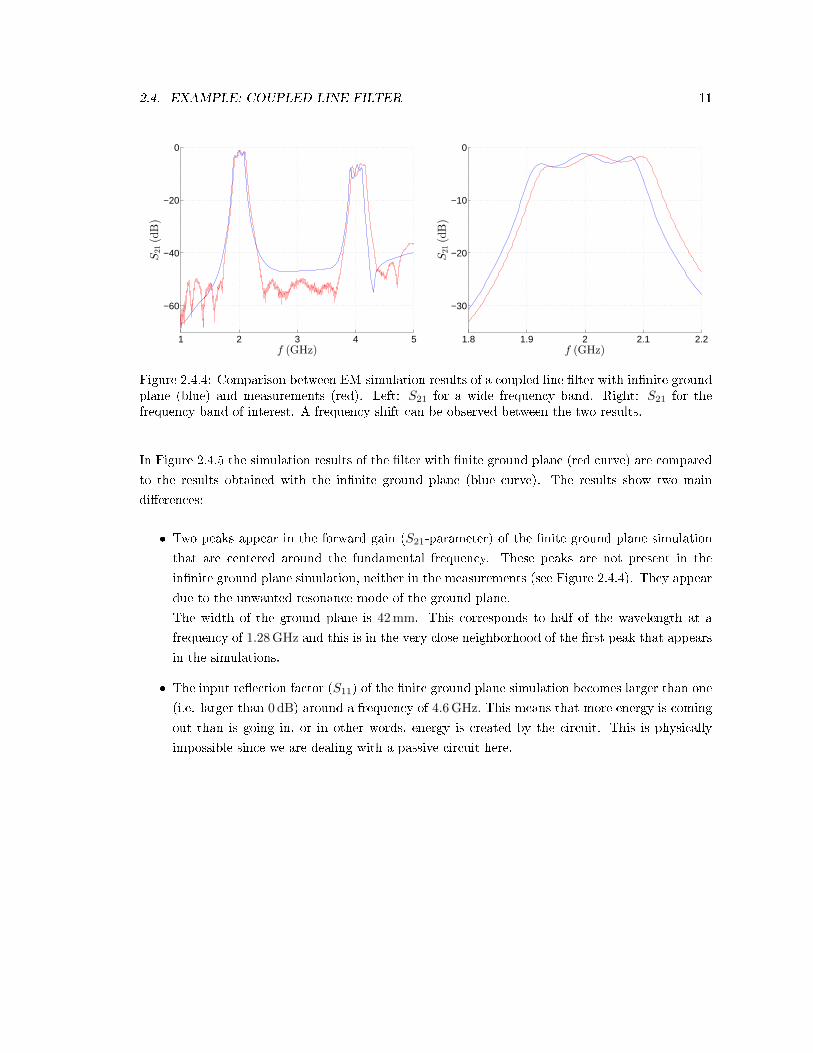
Figure 2.4.4: Comparison between EM-simulation results of a coupled line lter with innite groundplane (blue) and measurements (red). Left: S21 for a wide frequency band. Right: S21 for thefrequency band of interest. A frequency shift can be observed between the two results.
In Figure 2.4.5 the simulation results of the lter with nite ground plane (red curve) are compared
to the results obtained with the innite ground plane (blue curve). The results show two main
dierences:
Two peaks appear in the forward gain (S21-parameter) of the nite ground plane simulation
that are centered around the fundamental frequency. These peaks are not present in the
innite ground plane simulation, neither in the measurements (see Figure 2.4.4). They appear
due to the unwanted resonance mode of the ground plane.
The width of the ground plane is 42 mm. This corresponds to half of the wavelength at a
frequency of 1.28 GHz and this is in the very close neighborhood of the rst peak that appears
in the simulations.
The input reection factor (S11) of the nite ground plane simulation becomes larger than one
(i.e. larger than 0 dB) around a frequency of 4.6 GHz. This means that more energy is coming
out than is going in, or in other words, energy is created by the circuit. This is physically
impossible since we are dealing with a passive circuit here.
12 CHAPTER 2. SIMULATOR SETTINGS
1 2 3 4 5−25
−15
−5
5
f (GHz)
S11(dB)
1 2 3 4 5
−60
−40
−20
0
f (GHz)
S21(dB)
Figure 2.4.5: Comparison of the EM-simulation results of a coupled line lter with nite (red) andinnite ground plane (blue). Left: the input reection factor S11. Right: the forward gain S21. Forthe case of a nite ground plane we see an unrealistic behavior of S11 around a frequency of 4.6 GHz.Also, two peaks appear in the S21-parameter.
There is denitely something wrong with the simulation. When the simulations are started, it
is noticed that the simulator takes a very long time for calibrating the ports. Furthermore, two
warnings appear:
1. The 2D port solver data is not available, using default values (50 Ohm) for the transmission
line parameters
2. S-parameter results show unphysical behavior for certain frequencies. Cause:
inaccurate (high frequency) calibration;
mesh density is too coarse.
The causes that are proposed by ADS [3] and are not applicable to our case are not mentioned
above. If the mesh density is too coarse, this can be easily adjusted but it strongly increases the
simulation time. Another possible cause is a problem with the calibration. The problem is explained
as follows: the addition of the transmission line feed line at the ports does not necessarily include
an additional extension of the nite ground plane at the ports, causing an incorrect calibration.
Since the TML-calibration leads to unrealistic results, we opt for an uncalibrated port (calibration
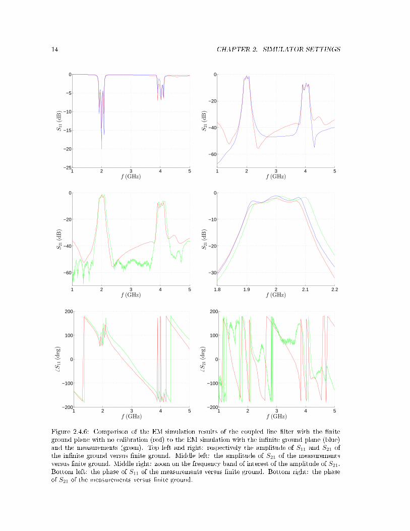
type: none). The results are shown in Figure 2.4.6.
Top left gure: The amplitude of S11 does not exceed 0 dB, thus the simulations do not show
unrealistic behavior this time.
evi.vannechel
Highlight
2.4. EXAMPLE: COUPLED LINE FILTER 13
Top right gure: There is a quite good in-band match of the amplitude of the S21-parameter
between the nite and the innite ground plane simulation. However, the out-of-band behavior
shows some large dierences.
Middle left gure: The amplitude of the S21-parameter of the nite ground plane simulation
also matches the measurements quite well in-band, but again some dierences are visible in
the out-of-band behavior.
Middle right gure: There is again a frequency shift of about 25 GHz between the simulations
and the measurements, but this was expected. We can also see that the bandwidth of both
simulations is smaller than the bandwidth of the measured lter. This is possibly due to
the fact that the mesh density was still too coarse and hence, the simulation results are not
accurate enough, although no warnings appeared.
Bottom left gure: The phase of S11 of the measurements and the nite ground plane sim-
ulation match almost perfectly, if the small frequency shift of about 25 GHz is taken into
account.
Bottom right gure: For the phase of S21 of the measurements and the nite ground plane
simulation there is only a good match around the center frequency and around the second
harmonic, taking the small frequency shift into account again. Out-of-band the phase does
not match, but this is expected since the out-of-band amplitude of S21 does not match either
(middle left gure).
We can state that there are still some details that the simulator can not simulate correctly or
accurately enough. This problem is explained as follows. The dielectric loss model that is used,
namely the Svensson/Djordjevic model, does not t the real dielectric losses of the substrate that is
used. This is where the small dierences in simulations and measurements come from. Up to 5 GHz
these deviations are still acceptable. Since no better alternative dielectric loss model is found, the
Svensson/Djordjevic model is used for all future simulations.
2.4.3 Conclusion
We conclude that the ports must be uncalibrated in order to obtain realistic simulations when
simulating a nite ground plane. For the settings concerning the simulation mode, the mesh and
the substrate we refer to Sections 2.4.1.1, 2.4.1.2, 2.4.1.4 and 2.3.
These are the settings that are used for all the following examples in this thesis, unless it is explicitly
mentioned dierently.
evi.vannechel
Highlight
14 CHAPTER 2. SIMULATOR SETTINGS
1 2 3 4 5−25
−20
−15
−10
−5
0
f (GHz)
S11(dB)
1 2 3 4 5
−60
−40
−20
0
f (GHz)
S21(dB)
1 2 3 4 5
−60
−40
−20
0
f (GHz)
S21(dB)
1.8 1.9 2 2.1 2.2
−30
−20
−10
0
f (GHz)
S21(dB)
1 2 3 4 5−200
−100
0
100
200
f (GHz)
6S11(deg)
1 2 3 4 5−200
−100
0
100
200
f (GHz)
6S21(deg)
Figure 2.4.6: Comparison of the EM-simulation results of the coupled line lter with the niteground plane with no calibration (red) to the EM-simulation with the innite ground plane (blue)and the measurements (green). Top left and right: respectively the amplitude of S11 and S21 ofthe innite ground versus nite ground. Middle left: the amplitude of S21 of the measurementsversus nite ground. Middle right: zoom on the frequency band of interest of the amplitude of S21.Bottom left: the phase of S11 of the measurements versus nite ground. Bottom right: the phaseof S21 of the measurements versus nite ground.
Chapter 3
Modeling a microstrip line with
slotted ground plane
3.1 Introduction
This chapter examines the eects of rectangular slots in the ground plane on the frequency response
of a single transmission line. Since the aim is to use these slotted ground plane structures in lter
designs, models are generated to predict these eects. Such models facilitate the design in two ways:
they dene an equivalent circuit that can be used in the synthesis; they provide a cheap alternative
to the numerically expensive EM-simulation (electromagnetic simulation) of Momentum [2] that can
be used to ne-tune the lter or determine the sensitivity of the frequency response function (FRF)
to geometric inaccuracies. The key idea is that this allows to predict the behavior of the design.
The model can then be used as a starting point for our future designs. This is a very important
step towards a proper design procedure since it allows us to make a design that is based on some
fundamental synthesis rather than merely using expensive overnight EM-based optimizations.
Section 3.2 describes the geometry for a single transmission line with slots in the ground plane
underneath it. Section 3.3 discusses a lumped-element equivalent circuit model, introduced in [9].
The model is studied by use of an example (Section 3.4). The EM-simulations, the lumped model
and the measurements of the realized design are compared next. The obtained result is not very
satisfactory since the lumped circuit model is not complex enough to model the structure.
The design is reduced to a transmission line with only one slot in the ground plane in order to restrict
the complexity of the structure (Section 3.5). After the improvements proposed in Sections 3.5.3,
3.5.4 and 3.5.5, the lumped circuit model predicts anti-resonances and quality factors accurately and
is symmetric, which is not the case for the original lumped circuit model. Section 3.6 discusses a
parametric multiple-input-multiple-output (MIMO) model for this one-slot structure to verify how
15
16 CHAPTER 3. MODELING A MICROSTRIP LINE WITH SLOTTED GROUND PLANE
good the improved lumped model represents the transmission line structure by comparing the poles
and zeros.
3.2 Single microstrip line with rectangular slots
The geometry of the structure used in Chapter 3 consists of a single microstrip line with rectangular
slots in the ground plane underneath it (Figure 3.2.1a). The width of the microstrip line is W . The
slots have a length d and a width Ws. The distance between the center of the slots is p. To model
this structure, we consider that it consists of a periodic repetition of an elementary cell as shown in
Figure 3.2.1b. The distance p is also used as the length of the cell. The number of slots is chosen
equal to N .
(a) (b) (c)
Figure 3.2.1: (a): Symmetrical slotted ground plane structure with N = 11. (b): Symmetrical unitcell of length p with slot width Ws, slot length d and microstrip line width W . (c): General unitcell of length p with slot width Ws, slot length d = d1 + d2 and microstrip line width W .
Figure 3.2.1c shows a slot that is coupled asymmetrically with respect to the line, i.e. the slotline
is not fed in its center. In that case, the length of the slot, d, should be split into two parts: d1 and
d2. These lengths are, respectively, the lengths of the slot that are situated 'above' and 'below' the
microstrip line.
This asymmetrical unit cell (Figure 3.2.1c) is more general than the previous one (Figure 3.2.1b)
since it contains the symmetrical case when d1 = d2. Therefore, this unit cell is used as the general
one for the remainder of the text. The inuence of the feedpoint of the slotline is discussed in
Section 3.4.2, when a lumped-element equivalent circuit model is proposed for the general unit cell.
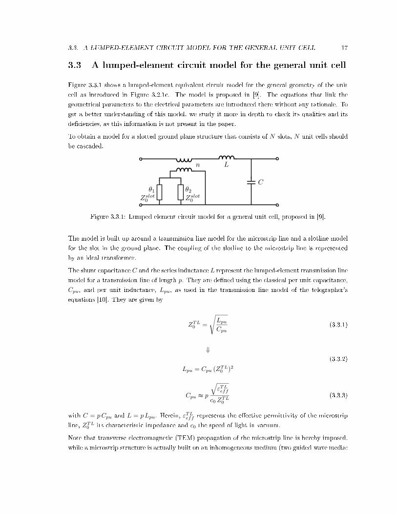
3.3. A LUMPED-ELEMENT CIRCUIT MODEL FOR THE GENERAL UNIT CELL 17
3.3 A lumped-element circuit model for the general unit cell
Figure 3.3.1 shows a lumped-element equivalent circuit model for the general geometry of the unit
cell as introduced in Figure 3.2.1c. The model is proposed in [9]. The equations that link the
geometrical parameters to the electrical parameters are introduced there without any rationale. To
get a better understanding of this model, we study it more in-depth to check its qualities and its
deciencies, as this information is not present in the paper.
To obtain a model for a slotted ground plane structure that consists of N slots, N unit cells should
be cascaded.
Figure 3.3.1: Lumped-element circuit model for a general unit cell, proposed in [9].
The model is built up around a transmission line model for the microstrip line and a slotline model
for the slot in the ground plane. The coupling of the slotline to the microstrip line is represented
by an ideal transformer.
The shunt capacitance C and the series inductance L represent the lumped-element transmission line
model for a transmission line of length p. They are dened using the classical per unit capacitance,
Cpu, and per unit inductance, Lpu, as used in the transmission line model of the telegrapher's
equations [10]. They are given by
ZTL0 =
√LpuCpu
(3.3.1)
⇓
Lpu = Cpu (ZTL0 )2(3.3.2)
Cpu ≈ p
√εTLeff
c0 ZTL0
(3.3.3)
with C = pCpu and L = pLpu. Herein, εTLeff represents the eective permittivity of the microstrip
line, ZTL0 its characteristic impedance and c0 the speed of light in vacuum.
Note that transverse electromagnetic (TEM) propagation of the microstrip line is hereby imposed,
while a microstrip structure is actually built on an inhomogeneous medium (two guided-wave media:
18 CHAPTER 3. MODELING A MICROSTRIP LINE WITH SLOTTED GROUND PLANE
dielectric and air). Hence, a microstrip line does not support a true TEM-wave. The propagation
of the elds along a microstrip line can be approximated by TEM-propagation, which is called
the quasi-TEM approximation. The inhomogeneous medium is then replaced by a homogeneous
medium with an eective permittivity εeff (as is done in Equation (3.3.3)). Note that the eective
permittivity is calculated dierently for a microstrip line (Equation (3.3.4)) and a slotline ([11]).
The microstrip line is also dispersive, which means that its characteristic impedance varies with the
frequency. This implies that Equation (3.3.1) is an approximation for√
Rpu+jωLpu
Gpu+jωCpu, which is only
valid if we assume that the line is lossless. Since the losses of the microstrip line are suciently low,
this approximation holds.
The quasi-static characteristic impedance of the line can be calculated by using the Wheeler closed-
form approximations [12]. The characteristic impedance is determined by the width of the microstrip
line, W , the thickness of the substrate, h, and the eective permittivity of the microstrip line, εTLeff .
The quasi-static characteristic impedance is calculated dierently for wide and for narrow microstrip
lines with respect to the thickness of the substrate using an empirical law.
For narrow microstrip lines (Wh < 1) ZTL0 is calculated by
ZTL0 =60√εTLeff
ln
(8h
W+ 0.25
W
h
)
and for wide strips (Wh ≥ 1) by
ZTL0 =120π√
εTLeff[Wh + 1.393 + 2
3 ln(Wh + 1.44
)]with
εTLeff =εr + 1
2+εr − 1
2
(1 +
10h
W
)−0.5(3.3.4)
The slotline in this circuit is represented by an ideal transmission line, or delay line, that is connected
to ground on both sides and tapped along the line to a transformer as in Figure 3.3.1. The position
of the tap in the circuit model corresponds to the position of the feedpoint of the slotline in the
transmission line structure. The tapped delay line has an electrical length θ = θ1 +θ2, where θ1 and
θ2 dene the position of the tap. They are expressed in radians and dened at a reference frequency
fref , that corresponds to the rst resonance frequency of the slotline.
The electrical length is dened as the product of the propagation constant, βslotm , and the length of
the slot, d1 or d2:
θ1,2 = βslotm d1,2 (3.3.5)
3.4. EXAMPLE: TRANSMISSION LINE WITH SLOTTED GROUND PLANE 19
with
βslotm =ωmvϕ
=2π fmc0√
εsloteff µr
(3.3.6)
fm ≈ mc0
2 d√εsloteff
(3.3.7)
Herein, vϕ represents the phase velocity, d = d1 + d2, m the mth resonance mode of the slotline,
fm the mth resonance frequency of the slotline, εsloteff the eective permittivity of the slotline and µr
the relative permeability of the substrate, which can be considered equal to 1. Note that Equation
(3.3.7) is dened in [9] as an approximation.
An ideal transformer is used to represent the coupling between the slotline and the microstrip line.
The turns ratio of the transformer, n , is dened as
n =
√ZsourceZload
It is approximated in [9] by
n ≈
√ZTL0
Zslot0
(3.3.8)
with Zslot0 the characteristic impedance of the slotline.
Note that TEM-propagation of the slotline is hereby imposed, while the mode of propagation in a
slotline is actually non-TEM as it is almost transverse electric (TE). Hence, the slotline is strongly
dispersive which means Zslot0 strongly varies with the frequency: Zslot0 (f). As mentioned before,
the microstrip line is also dispersive. As a result, n also strongly varies with the frequency: n(f).
Therefore, Equation (3.3.8) is a rather weak approximation. Paper [9] includes a graph showing the
large variety of Zslot0 (f) and n(f). It is suggested to use the values of Zslot0 (f) and n(f) at the rst
resonance frequency to limit the eect of the dispersion.
The characteristic impedance of the slotline Zslot0 and its eective permittivity εsloteff are calculated
by using [11]. In this paper, dierent cases for calculating Zslot0 and εsloteff are proposed, depending
on the relative permittivity of the substrate, εr, the width of the slotline, Ws, and the free space
wavelength at the rst resonance frequency, λ0. We are in the case
2.22 ≤ εr ≤ 3.8 and 0.0015 ≤ Ws
λ0≤ 0.075
3.4 Example: transmission line with slotted ground plane
This section discusses the use and the properties of the previously described model using an example.
The response of the EM-simulations and the corresponding circuit model are compared. The results
20 CHAPTER 3. MODELING A MICROSTRIP LINE WITH SLOTTED GROUND PLANE
of this study allow to draw some conclusions about the usefulness and the correctness of the model.
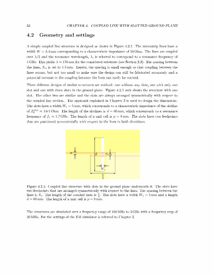
3.4.1 Geometry and settings
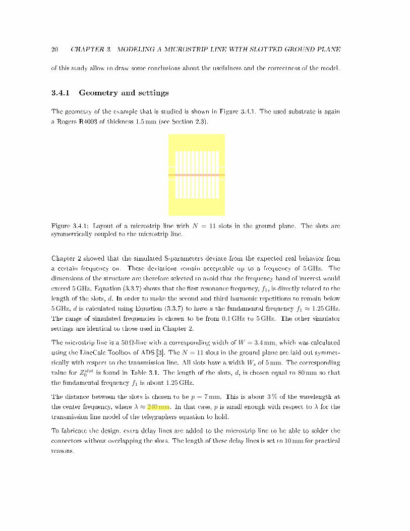
The geometry of the example that is studied is shown in Figure 3.4.1. The used substrate is again
a Rogers R4003 of thickness 1.5 mm (see Section 2.3).
Figure 3.4.1: Layout of a microstrip line with N = 11 slots in the ground plane. The slots aresymmetrically coupled to the microstrip line.
Chapter 2 showed that the simulated S-parameters deviate from the expected real behavior from
a certain frequency on. These deviations remain acceptable up to a frequency of 5 GHz. The
dimensions of the structure are therefore selected to avoid that the frequency band of interest would
exceed 5 GHz. Equation (3.3.7) shows that the rst resonance frequency, f1, is directly related to the
length of the slots, d. In order to make the second and third harmonic repetitions to remain below
5 GHz, d is calculated using Equation (3.3.7) to have a the fundamental frequency f1 ≈ 1.25 GHz.
The range of simulated frequencies is chosen to be from 0.1 GHz to 5 GHz. The other simulator
settings are identical to those used in Chapter 2.
The microstrip line is a 50 Ω-line with a corresponding width of W = 3.4 mm, which was calculated
using the LineCalc Toolbox of ADS [3]. The N = 11 slots in the ground plane are laid out symmet-
rically with respect to the transmission line. All slots have a width Ws of 5 mm. The corresponding
value for Zslot0 is found in Table 3.1. The length of the slots, d, is chosen equal to 80 mm so that
the fundamental frequency f1 is about 1.25 GHz.
The distance between the slots is chosen to be p = 7 mm. This is about 3 % of the wavelength at
the center frequency, where λ ≈ 240 mm. In that case, p is small enough with respect to λ for the
transmission line model of the telegraphers equation to hold.
To fabricate the design, extra delay lines are added to the microstrip line to be able to solder the
connectors without overlapping the slots. The length of these delay lines is set to 10 mm for practical
reasons.
evi.vannechel
Highlight
evi.vannechel
Callout
dit is niet de guided wavelength!! hier gewoon c/f
3.4. EXAMPLE: TRANSMISSION LINE WITH SLOTTED GROUND PLANE 21
The corresponding lumped model circuit is shown in Figure 3.4.2. The lumped model-block repre-
sents the unit cell of Section 3.3 and is repeated N = 11 times. The model parameters are given
in Table 3.1. Parameters C, L, f1 and n are calculated from Equations (3.3.3), (3.3.2), (3.3.7) and
(3.3.8) respectively. For the equation for parameter Zslot0 we refer to [11].
The extra delay lines that were added to the distributed design are also included in the model (see
Figure 3.4.2) in order to be able to compare the two simulations. These lines have a characteristic
impedance Z0 of 50 Ω and an electrical length θ that corresponds to a physical length of 10 mm.
Figure 3.4.2: The complete lumped circuit model that corresponds to the distributed design inFigure 3.4.1.
3.4.2 Lumped-element circuit model vs. EM-simulations
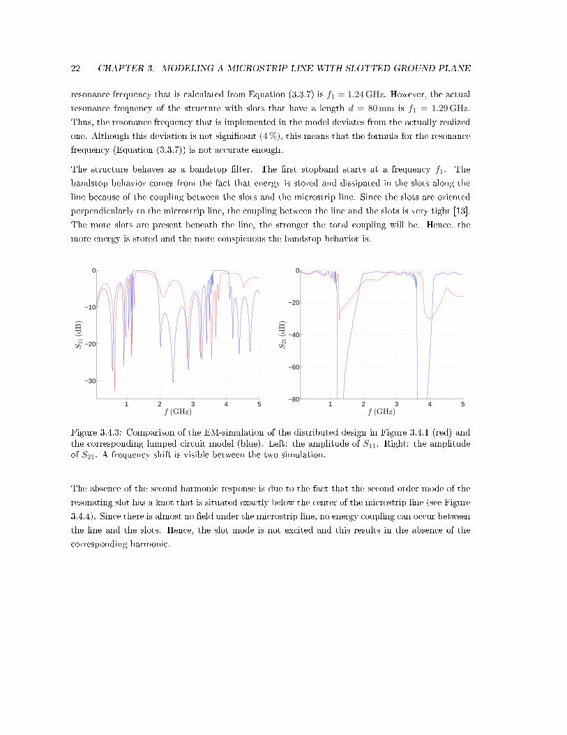
Figure 3.4.3 compares the reection and the transmission properties of the EM-simulations (red)
and the lumped model (blue). The resonance frequency of the transmission line circuit is about 4 %
higher than the one that is calculated for the model via Equation (3.3.7), relative to the expected
resonance frequency of the lumped circuit model. For a slotline with a length d = 80 mm, the
22 CHAPTER 3. MODELING A MICROSTRIP LINE WITH SLOTTED GROUND PLANE
resonance frequency that is calculated from Equation (3.3.7) is f1 = 1.24 GHz. However, the actual
resonance frequency of the structure with slots that have a length d = 80 mm is f1 = 1.29 GHz.
Thus, the resonance frequency that is implemented in the model deviates from the actually realized
one. Although this deviation is not signicant (4 %), this means that the formula for the resonance
frequency (Equation (3.3.7)) is not accurate enough.
The structure behaves as a bandstop lter. The rst stopband starts at a frequency f1. The
bandstop behavior comes from the fact that energy is stored and dissipated in the slots along the
line because of the coupling between the slots and the microstrip line. Since the slots are oriented
perpendicularly to the microstrip line, the coupling between the line and the slots is very tight [13].
The more slots are present beneath the line, the stronger the total coupling will be. Hence, the
more energy is stored and the more conspicuous the bandstop behavior is.
1 2 3 4 5
−30
−20
−10
0
f (GHz)
S11(dB)
1 2 3 4 5−80
−60
−40
−20
0
f (GHz)
S21(dB)
Figure 3.4.3: Comparison of the EM-simulation of the distributed design in Figure 3.4.1 (red) andthe corresponding lumped circuit model (blue). Left: the amplitude of S11. Right: the amplitudeof S21. A frequency shift is visible between the two simulation.
The absence of the second harmonic response is due to the fact that the second order mode of the
resonating slot has a knot that is situated exactly below the center of the microstrip line (see Figure
3.4.4). Since there is almost no eld under the microstrip line, no energy coupling can occur between
the line and the slots. Hence, the slot mode is not excited and this results in the absence of the
corresponding harmonic.
3.4. EXAMPLE: TRANSMISSION LINE WITH SLOTTED GROUND PLANE 23
Figure 3.4.4: Transmission line with slots in the ground plane, showing the rst three resonancemodes of the slots and their knots, where the electrical eld is zero.
More generally, this means that we can choose, up to some level, which harmonics we want to excite
and which ones we want to avoid. This is a very nice feature that can be used to lter some harmonic
responses. The third harmonic, for example, is not excited if we position the slots asymmetrically
with respect to line. More specically if the feedpoint of the slotline lies at one third instead of in
its center (see Figure 3.4.5).
Figure 3.4.5: Transmission line with a slot in the ground plane that is coupled at one third of theline. Hence, the feedpoint coincides with a knot of the third mode. This implies that the third modewill not be excited.
Theoretically, the electrical eld underneath the transmission line then becomes zero. In practice
however, the eld will not be exactly zero because the smallest inaccuracy during the fabrication
24 CHAPTER 3. MODELING A MICROSTRIP LINE WITH SLOTTED GROUND PLANE
process can cause that the slot is not perfectly aligned. Hence in practice, the mode will be slightly
hit.
To compensate for the frequency shift that was shown earlier we can manually apply a rst order
frequency correction to the model elements. This correction only aects the reference frequency
for the electrical lengths of the ideal transmission lines in the model (Figure 3.3.1). The results
obtained after the frequency correction are shown in Figure 3.4.6.
From 0.1 GHz up to the rst resonance frequency, f1 ≈ 1.3 GHz, the model ts the results quite
well. This is shown by the error (gray -.-) that is plotted on the amplitude plots of S11 and S21 (top
gures of Figure 3.4.6). The peaks in the error show that the resonance frequencies of the circuit
model and the EM-simulations are still a little bit dierent in this frequency band.
From f1 = 1.3 GHz to about 2 GHz the rst stopband is visible. After the frequency compensa-
tion, the resonance frequency of the slotline in the EM-simulation is now equal to the one of the
corresponding delay line in the circuit model. The slopes at the edge of the stopband of the two
simulations however, still dier signicantly. The slope of the model is much steeper than the
slope of the EM-simulation. This means the quality factor of the resonator is much higher in the
model compared to the EM-simulation. The 3 dB-bandwidth of the two simulations also diers
signicantly.
In the stopband, the attenuation of the circuit model is several orders of magnitude higher than
the attenuation of the EM-simulation. This indicates that the model does not take any losses into
account. This is also clearly visible in the plot of the S11-parameter where almost everything is
reected in the stopband.
The match of the ripple in front of the second resonance is not as good as for the ripple before the
rst resonance. However, this can be improved by tuning the parameters of the model. The quality
of the t of the second resonance is similar to the t of the rst resonance.
A root-mean-square error (RMSE), as dened in Equation (3.4.1), of about −11 dB and −9.5 dB is
obtained over the frequency band of interest for S11 and S21 respectively, which is still high for a
good quality model. This indicates that the overall t is not that good.
RMSESij=
√√√√ 1
N
N∑f=1
[Sij, sim(f)− Sij,mod(f)]2
(3.4.1)
When looking at the phase of S11 and S21 (middle gures), the same observations can be made
as for the amplitudes. The frequency bands right before the resonances show a very good match.
However, from the rst resonance frequency on, the phase of the S-parameters of the circuit model
does not match the EM-simulations anymore. This is also clearly visible when the S-parameters are
plotted on a Smith Chart (bottom gures). On the Smith Charts, only the rst resonance (from
0.5 GHz to 2 GHz) is shown to prevent that the plot would become unreadable.
3.4. EXAMPLE: TRANSMISSION LINE WITH SLOTTED GROUND PLANE 25
1 2 3 4 5−40
−30
−20
−10
0
f (GHz)
S11(dB)
1 2 3 4 5−80
−60
−40
−20
0
f (GHz)
S21(dB)
1 2 3 4 5−300
−200
−100
0
100
f (GHz)
6S11(deg)
1 2 3 4 5−300
−200
−100
0
100
f (GHz)
6S21(deg)
0.2
0.5
1.0
2.0
5.0
+j0.2
−j0.2
+j0.5
−j0.5
+j1.0
−j1.0
+j2.0
−j2.0
+j5.0
−j5.0
0.0 ∞ 0.2
0.5
1.0
2.0
5.0
+j0.2
−j0.2
+j0.5
−j0.5
+j1.0
−j1.0
+j2.0
−j2.0
+j5.0
−j5.0
0.0 ∞
Figure 3.4.6: Comparison of the EM-simulations of the distributed design in Figure 3.4.1 (red) andthe corresponding lumped model with corrected resonance frequency (blue). Top left: the amplitudeof S11 and the error (gray -.-). Top right: the amplitude of S21 and the error (gray -.-). Middle left:the phase of S11. Middle right: the phase of S21. Bottom left: S11-parameter plotted on the SmithChart. Bottom right: S21-parameter plotted on the Smith Chart. The ripple is matched very well.The bad match of the stopband shows that the model does not capture the stopband behavior.
26 CHAPTER 3. MODELING A MICROSTRIP LINE WITH SLOTTED GROUND PLANE
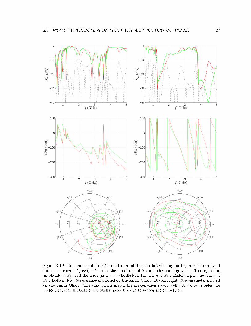
Figure 3.4.7 compares the simulations to the measurements. Besides some unwanted extra ripples
that are present between 0.1 GHz and 0.8 GHz, the EM-simulations predict the real behavior (mea-
surements) very well. This is veried when looking at the error that is plotted in gray (-.-) (top
gures). Again, the high peaks in the error are explained by a small dierence in the resonance
frequencies of the circuit model and the EM-simulations. An RMSE of about −18 dB and −19 dB is
obtained over the whole frequency band for S11 and S21 respectively, which is denitely acceptable.
The stray ripples present in the measurements can be due to a lower accuracy of the calibration
of the vector network analyzer (VNA) or to the presence of more than one EM-mode, as this can
indeed be present in the real circuit but is not simulated by the EM-simulator.
Both the amplitude as well as the phase show a very good match. This is conrmed when comparing
the S-parameters on a Smith Chart. Again, only the rst resonance (from 0.5 GHz to 2 GHz) is shown
to prevent that the plot would become too complex.
Since we are not satised with the quality we obtain with the current model, we will try to improve
it by tuning the model parameters (Sections 3.4.3).
3.4. EXAMPLE: TRANSMISSION LINE WITH SLOTTED GROUND PLANE 27
1 2 3 4 5−40
−30
−20
−10
0
f (GHz)
S11(dB)
1 2 3 4 5−40
−30
−20
−10
0
f (GHz)
S21(dB)
1 2 3 4 5−300
−200
−100
0
100
f (GHz)
6S11(deg)
1 2 3 4 5−300
−200
−100
0
100
f (GHz)
6S21(deg)
0.2
0.5
1.0
2.0
5.0
+j0.2
−j0.2
+j0.5
−j0.5
+j1.0
−j1.0
+j2.0
−j2.0
+j5.0
−j5.0
0.0 ∞ 0.2
0.5
1.0
2.0
5.0
+j0.2
−j0.2
+j0.5
−j0.5
+j1.0
−j1.0
+j2.0
−j2.0
+j5.0
−j5.0
0.0 ∞
Figure 3.4.7: Comparison of the EM-simulations of the distributed design in Figure 3.4.1 (red) andthe measurements (green). Top left: the amplitude of S11 and the error (gray -.-). Top right: theamplitude of S21 and the error (gray -.-). Middle left: the phase of S11. Middle right: the phase ofS21. Bottom left: S11-parameter plotted on the Smith Chart. Bottom right: S21-parameter plottedon the Smith Chart. The simulations match the measurements very well. Unwanted ripples arepresent between 0.1 GHz and 0.8 GHz, probably due to inaccurate calibration.
28 CHAPTER 3. MODELING A MICROSTRIP LINE WITH SLOTTED GROUND PLANE
3.4.3 Tuned lumped-element circuit model vs. EM-simulations
In an attempt to improve the model, the parameters of the lumped-element circuit model are tuned.
Our goal is to decrease the slope that sets the selectivity and decrease the attenuation of the circuit
model in the rst stopband. At the same time, we want to keep the description of the ripple as it
is.
Figure 3.4.8 shows that the slope can be decreased signicantly by decreasing the capacitor and
inductor value and the value of the turns ratio. After tuning, the slope matches the EM-simulation
quite well. However, the match of the ripple is gone. This is because the ripple is mainly due
to the LC-circuit. Changing the capacitor and inductor values therefore changes the ripple. The
disadvantage is that the slope could not be decreased without changing L or C. Furthermore, the
attenuation in the stopband is not changed. Hence, improving one part of our goal, deteriorates the
quality of the other parts.
1 2 3 4 5
−30
−20
−10
0
f (GHz)
S11(dB)
1 2 3 4 5−80
−60
−40
−20
0
f (GHz)
S21(dB)
Figure 3.4.8: Comparison of the EM-simulations of the distributed design in Figure 3.4.1 (red) andthe corresponding tuned, lumped model (blue). Left: the amplitude of S11. Right: the amplitudeof S21. The match of the slope is better, at the cost of the match of the ripple.
The parameter values that are achieved for the tuned model are given in Table 3.2.
We can conclude that there are some fundamental issues with the proposed circuit model. The
advantage is that the ripple is modeled very well. However, the model does not properly predict the
real in-band behavior of the system. The two main issues are the poor modeling performance of the
losses and the quality factor that the model proposes. The fact that the quality factor of the model
is too high can be attributed to the fact that the transformer is ideal while the coupling between
the slots and the line is not.
The proposed circuit model has also some other shortcomings. As was already mentioned in Section
3.3, the transmission line and the slotline are dispersive because the microstrip structure is built
on an inhomogeneous dielectric medium (two guided-wave media: dielectric and air). The value of
the turns ratio, n, proposed for the transformer by an empirical law, dened by Equation (3.3.8), is
therefore a very weak approximation.
Secondly, the representation of the transmission line by the series inductance and shunt capacitance
is actually only valid for an innitesimal slice of the transmission line or for a transmission line
used below the rst resonance. Here, the LC-equivalent must represent a transmission line slice, p,
of 7 mm, which corresponds to about λ/35 at the center frequency. Since p is about 1.5 orders of
magnitude smaller than λ, this approximation is neither strong nor weak.
Furthermore, there is the fact that we needed to carry out a frequency correction in order to get
the frequency right. All these factors play a signicant role in the quality of the model.
We cannot reach our goal only by tuning the model parameters. Therefore, we will try a dierent
approach. In order to get more insight in the behavior of the structure, we reduce the complexity
of the model structure. To keep the structure as simple as possible, a transmission line with only
one slot in the ground plane is studied. Section 3.5 compares the EM-simulation of this one-slot
structure to the lumped-element circuit model from paper [9].
3.5 Simplied structure: a single slot
Since the previous attempt to t the lumped-element circuit model to the EM-simulations was not
very successful, we take one step back. Instead of using a design with multiple slots, we restrict
ourselves to a single slot structure.
3.5.1 Geometry and settings
The geometry of the single slot structure is shown in Figure 3.5.1. The same dimensions are used as
in Section 3.4.1 (see Table 3.1). The only model parameter that is changed is the number of slots,
N , which is set to 1 here. In the transmission line structure, the length of the extra delay-lines is
increased to 50 mm so that the length of the transmission line is larger than the length of the slot.
30 CHAPTER 3. MODELING A MICROSTRIP LINE WITH SLOTTED GROUND PLANE
Figure 3.5.1: Layout of a microstrip line with one slot in the ground plane underneath it.
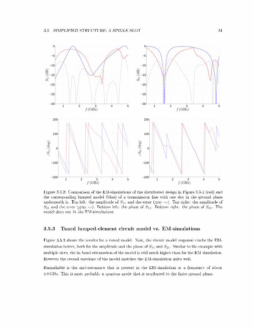
3.5.2 Lumped-element circuit model vs. EM-simulations
Figure 3.5.2 shows the EM-simulation (red) and the lumped model (blue) from 0.5 GHz to 5.5 GHz.
Surprisingly, the resonance frequency of the EM-simulated system is shifted to f1 = 1.6 GHz, while
it was expected to be at 1.3 GHz. The actual resonance frequency is now about 20 % higher than
expected, which is a big deviation. It is obvious that the resonance frequency f1, depends on the
number of slots, N , since this is the only parameter that is changed. In paper [9], however, in the
model there is no dependence of the resonance frequency on N (Equation (3.3.7)). This proves
again that the model is not accurate enough to be used for a practical design.
To properly compare the EM-simulation and the lumped model, a frequency correction was carried
out to compensate for the frequency shift in the same way as in Section 3.4.2. The results of the
lumped model without this correction are not useful. Hence, Figure 3.5.2 immediately shows the
lumped model with the correction applied.
Again, the results are not very satisfactory. Keeping in mind that a frequency correction was
needed beforehand, we can conclude that the model does not t the EM-simulations well. Both
the amplitude and the phase show a large mismatch. An RMSE of about −12 dB and −10 dB is
obtained over the whole frequency band for S11 and S21 respectively, which is again too high. The
error is plotted in gray (-.-) on the amplitude gures. We will again try to improve the t by tuning
the model parameters.
3.5. SIMPLIFIED STRUCTURE: A SINGLE SLOT 31
1 2 3 4 5−30
−25
−20
−15
−10
−5
0
f (GHz)
S11(dB)
1 2 3 4 5−30
−25
−20
−15
−10
−5
0
f (GHz)
S21(dB)
1 2 3 4 5−200
−100
0
100
200
f (GHz)
6S11(deg)
1 2 3 4 5−200
−100
0
100
200
f (GHz)
6S21(deg)
Figure 3.5.2: Comparison of the EM-simulations of the distributed design in Figure 3.5.1 (red) andthe corresponding lumped model (blue) of a transmission line with one slot in the ground planeunderneath it. Top left: the amplitude of S11 and the error (gray -.-). Top right: the amplitude ofS21 and the error (gray -.-). Bottom left: the phase of S11. Bottom right: the phase of S21. Themodel does not t the EM-simulations.
3.5.3 Tuned lumped-element circuit model vs. EM-simulations
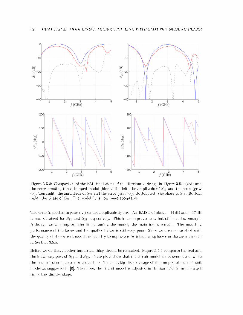
Figure 3.5.3 shows the results for a tuned model. Now, the circuit model response tracks the EM-
simulation better, both for the amplitude and the phase of S11 and S21. Similar to the example with
multiple slots, the in-band attenuation of the model is still much higher than for the EM-simulation.
However the overall envelope of the model matches the EM-simulation quite well.
Remarkable is the anti-resonance that is present in the EM-simulation at a frequency of about
4.8 GHz. This is most probably a spurious mode that is attributed to the nite ground plane.
32 CHAPTER 3. MODELING A MICROSTRIP LINE WITH SLOTTED GROUND PLANE
1 2 3 4 5−40
−30
−20
−10
0
f (GHz)
S11(dB)
1 2 3 4 5−40
−30
−20
−10
0
f (GHz)
S21(dB)
1 2 3 4 5−200
−100
0
100
200
f (GHz)
6S11(deg)
1 2 3 4 5−200
−100
0
100
200
f (GHz)
6S21(deg)
Figure 3.5.3: Comparison of the EM-simulations of the distributed design in Figure 3.5.1 (red) andthe corresponding tuned lumped model (blue). Top left: the amplitude of S11 and the error (gray-.-). Top right: the amplitude of S21 and the error (gray -.-). Bottom left: the phase of S11. Bottomright: the phase of S21. The model t is now more acceptable.
The error is plotted in gray (-.-) on the amplitude gures. An RMSE of about −14 dB and −17 dB
is now obtained for S11 and S21 respectively. This is an improvement, but still not low enough.
Although we can improve the t by tuning the model, the main issues remain. The modeling
performance of the losses and the quality factor is still very poor. Since we are not satised with
the quality of the current model, we will try to improve it by introducing losses in the circuit model
in Section 3.5.5.
Before we do this, another important thing should be remarked. Figure 3.5.4 compares the real and
the imaginary part of S11 and S22. These plots show that the circuit model is not symmetric, while
the transmission line structure clearly is. This is a big disadvantage of the lumped-element circuit
model as suggested in [9]. Therefore, the circuit model is adjusted in Section 3.5.4 in order to get
rid of this disadvantage.
3.5. SIMPLIFIED STRUCTURE: A SINGLE SLOT 33
1 2 3 4 5−1
−0.5
0
0.5
1
f (GHz)
Re(Sii)
1 2 3 4 5−1
−0.5
0
0.5
1
Figure 3.5.4: Comparison of the S11- (green) and S22-parameter (blue) of the lumped-element circuitmodel. Top left: the real part of S11 (green) and S22 (blue). Top right: the imaginary part of S11
(green) and S22 (blue).
3.5.4 Symmetrizing the lumped-element circuit model
A big disadvantage of the original lumped-element circuit model is that it is asymmetric. Since the
transmission line structure is a passive structure with a symmetric geometry, it is clearly symmet-
rical. Therefore, an important step in improving the circuit model is to make it symmetrical too.
In order to do so, the LC-circuit, that represents the transmission line, is split in two equal parts
distributed around the slot, as is shown in Figure 3.5.5.
Figure 3.5.5: Lumped-element circuit model for a general unit cell that is made symmetrical.
Hereby, the value of the total capacitance and inductance should remain the same as before (Equa-
tions (3.3.3) and (3.3.2)). To fulll that, the values of the capacitors and the inductors, as dened
in Figure 3.5.5, should be halved:
C =pCpu
2≈ p
√εTLeff
2 c0 ZTL0
L =pLpu
2=pCpu (ZTL0 )2
2
evi.vannechel
Callout
voordeel: 1 LC structure only corresponds to p/2 anymore so assumption of Telegraphers equation that an LC piece represents infinitesimal small piece of TL is more fulfilled
34 CHAPTER 3. MODELING A MICROSTRIP LINE WITH SLOTTED GROUND PLANE
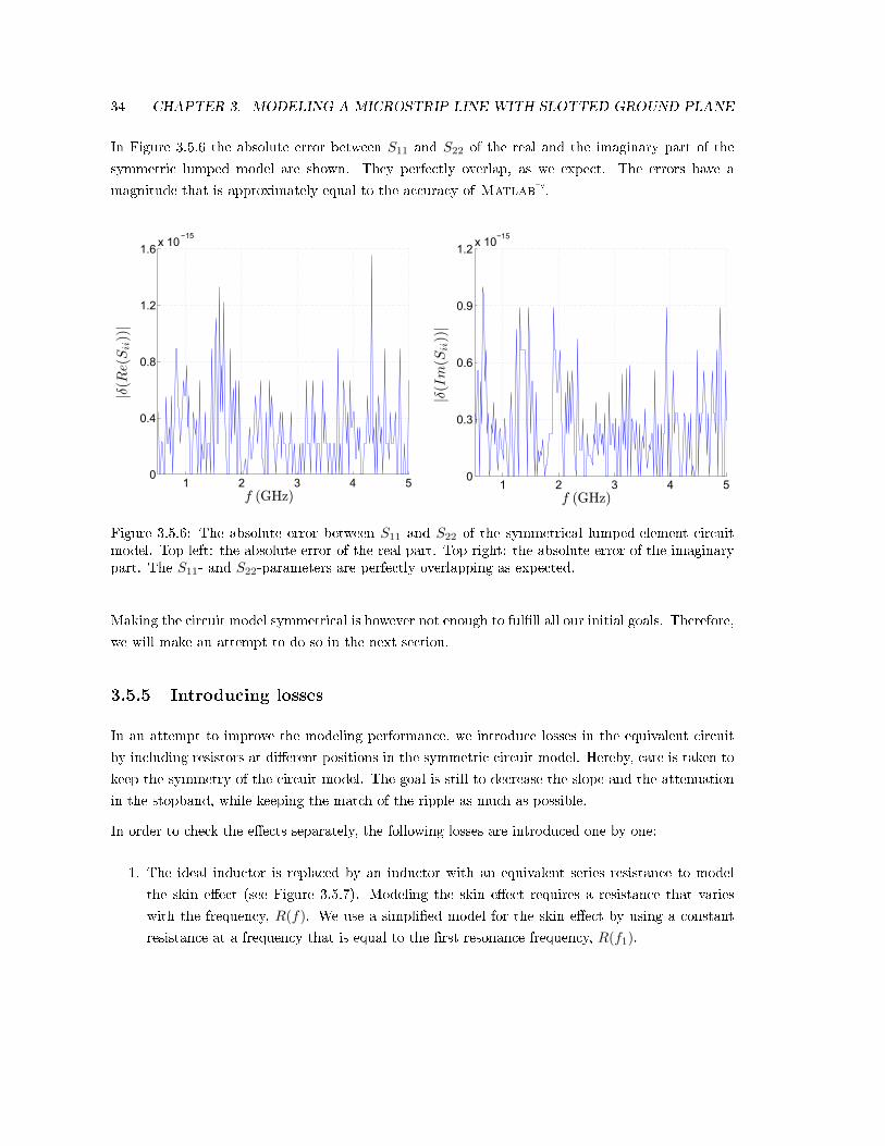
In Figure 3.5.6 the absolute error between S11 and S22 of the real and the imaginary part of the
symmetric lumped model are shown. They perfectly overlap, as we expect. The errors have a
magnitude that is approximately equal to the accuracy of Matlab.
1 2 3 4 50
0.4
0.8
1.2
1.6x 10
−15
f (GHz)1 2 3 4 5
0
0.3
0.6
0.9
1.2x 10
−15
f (GHz)
Figure 3.5.6: The absolute error between S11 and S22 of the symmetrical lumped-element circuitmodel. Top left: the absolute error of the real part. Top right: the absolute error of the imaginarypart. The S11- and S22-parameters are perfectly overlapping as expected.
Making the circuit model symmetrical is however not enough to fulll all our initial goals. Therefore,
we will make an attempt to do so in the next section.
3.5.5 Introducing losses
In an attempt to improve the modeling performance, we introduce losses in the equivalent circuit
by including resistors at dierent positions in the symmetric circuit model. Hereby, care is taken to
keep the symmetry of the circuit model. The goal is still to decrease the slope and the attenuation
in the stopband, while keeping the match of the ripple as much as possible.
In order to check the eects separately, the following losses are introduced one by one:
1. The ideal inductor is replaced by an inductor with an equivalent series resistance to model
the skin eect (see Figure 3.5.7). Modeling the skin eect requires a resistance that varies
with the frequency, R(f). We use a simplied model for the skin eect by using a constant
resistance at a frequency that is equal to the rst resonance frequency, R(f1).
3.5. SIMPLIFIED STRUCTURE: A SINGLE SLOT 35
Figure 3.5.7: Symmetrical lumped-element circuit model with a non-ideal inductor.
2. The ideal capacitor is replaced by a capacitor with an equivalent parallel resistance to model
the dielectric material losses (see Figure 3.5.8).
Figure 3.5.8: Symmetrical lumped-element circuit model with a non-ideal capacitance.
3. The two ideal transmission lines are replaced by equivalent microstrip lines with dielectric and
skin losses.
4. The LC-circuit is replaced by an equivalent microstrip line with dielectric and skin losses.
5. A resistor is added in series with the ideal transmission lines (see Figure 3.5.9) to model the
losses in the dielectric.
Figure 3.5.9: Symmetrical lumped-element circuit model with an additional resistor in series withthe ideal transmission lines.
6. A resistor is added in parallel with the whole circuit model (see Figure 3.5.10). This resistor
is added for the following reason. In the original, symmetrical circuit model the signal is com-
pletely reected at the resonance frequency. In the transmission line structure however this is
36 CHAPTER 3. MODELING A MICROSTRIP LINE WITH SLOTTED GROUND PLANE
not the case. By adding a resistor from the input to the output port, the total reection as
predicted by the circuit model disappears and the reection of the transmission line structure
can be modeled well.
Figure 3.5.10: Symmetrical lumped-element circuit model with an additional resistor in parallelwith the whole circuit model.
Trial (1) results in a decrease of the level of S11 and S21 over the whole frequency range, as shown
in Figure 3.5.11. Note that the result of the simulations with multiple slots is shown here because
the eect was more clear than in the simulations with only one slot. The slope of the stopband
transition is a bit less steep than before. This corresponds to an S11-parameter that decreases more
smoothly in the rst stopband (see rectangle in left gure). The match of the ripple is slightly better
(see rectangle in right gure). An RMSE of about −11 dB and −10 dB is obtained for S11 and S21
respectively, which is a small improvement compared to Figure 3.4.6.
1 2 3 4 5
−30
−20
−10
0
f (GHz)
S11(d
B)
1 2 3 4 5−80
−60
−40
−20
0
f (GHz)
S21(d
B)
Figure 3.5.11: Comparison of the EM-simulations of the distributed design in Figure 3.4.1 (red) andthe corresponding symmetrical lumped model with introduction of an equivalent series resistanceat the inductor (blue). Left: the amplitude of S11. Right: the amplitude of S21. The rectanglesindicate the improvements with respect to the lossless model from Figure 3.4.6.
3.5. SIMPLIFIED STRUCTURE: A SINGLE SLOT 37
Unfortunately, trials (2), (3) and (4) do not show a considerable improvement. Therefore, these
results are not shown and the adaptation of the circuit is not performed.
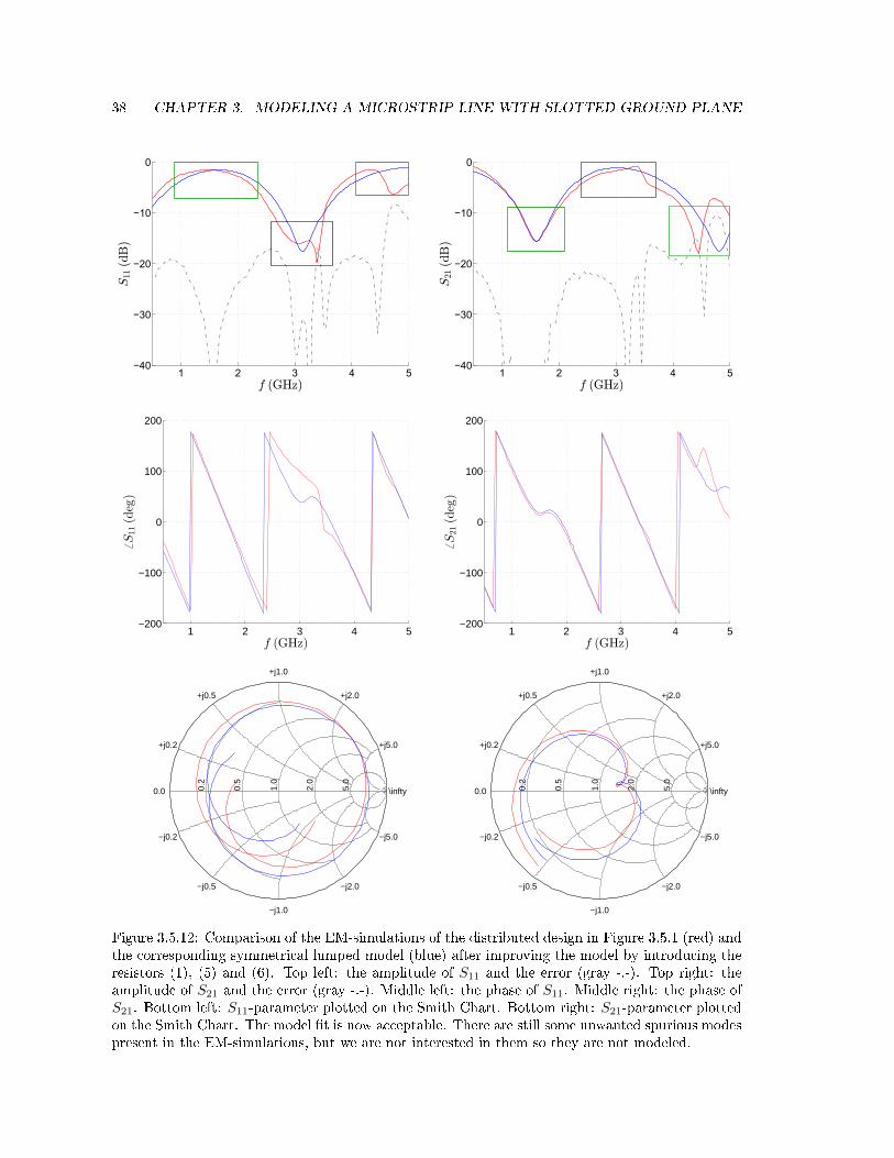
By introducing resistors (5) and (6), however, a considerable improvement is noticed. Adding a
resistor in series with the ideal transmission lines allows us to set the attenuation (see Figure 3.5.12,
top right), and hence also the reection (see Figure 3.5.12, top left), of the frequency band around
the resonance frequencies that are not excited (black rectangles). Adding a resistor in parallel with
the whole circuit model allows us to set the attenuation (see Figure 3.5.12, top right), and hence
also the reection (see Figure 3.5.12, top left), of the frequency bands around the excited resonance
frequencies (green rectangles).
Figure 3.5.12 shows the results after adding these two resistors and tuning the parameters. The
overall shape of the amplitude of S11 and S21 matches very well. Also the phase of both S11 and
S21 shows a very good match. Spurious modes are present at about 3.4 GHz and around 5 GHz.
These are attributed to the nite ground plane.
The slope of the circuit model now matches the slope of the EM-simulations. Also the attenuation
of the circuit model is decreased at the resonance frequencies. This means our two goals are now
reached. An RMSE of about −18 dB and −20 dB is obtained for S11 and S21 respectively, which
is a very big improvement compared to Figure 3.5.2 and an acceptable level. The S-parameters
are plotted on a Smith Chart in the bottom gures of Figure 3.5.12 over a range of 0.5 GHz to
2.5 GHz. Only the rst resonance is shown to prevent that the plot becomes too complex. The good
match of the improved lumped model and the EM-simulations is clearly visible. There are still some
unwanted spurious modes present in the EM-simulations, but since we believe they are due to the
nite ground plane eect, we will not try to model them.
38 CHAPTER 3. MODELING A MICROSTRIP LINE WITH SLOTTED GROUND PLANE
1 2 3 4 5−40
−30
−20
−10
0
f (GHz)
S11(d
B)
1 2 3 4 5−40
−30
−20
−10
0
f (GHz)
S21(d
B)
1 2 3 4 5−200
−100
0
100
200
f (GHz)
6S11(deg)
1 2 3 4 5−200
−100
0
100
200
f (GHz)
6S21(deg)
0.2
0.5
1.0
2.0
5.0
+j0.2
−j0.2
+j0.5
−j0.5
+j1.0
−j1.0
+j2.0
−j2.0
+j5.0
−j5.0
0.0 \infty 0.2
0.5
1.0
2.0
5.0
+j0.2
−j0.2
+j0.5
−j0.5
+j1.0
−j1.0
+j2.0
−j2.0
+j5.0
−j5.0
0.0 \infty
Figure 3.5.12: Comparison of the EM-simulations of the distributed design in Figure 3.5.1 (red) andthe corresponding symmetrical lumped model (blue) after improving the model by introducing theresistors (1), (5) and (6). Top left: the amplitude of S11 and the error (gray -.-). Top right: theamplitude of S21 and the error (gray -.-). Middle left: the phase of S11. Middle right: the phase ofS21. Bottom left: S11-parameter plotted on the Smith Chart. Bottom right: S21-parameter plottedon the Smith Chart. The model t is now acceptable. There are still some unwanted spurious modespresent in the EM-simulations, but we are not interested in them so they are not modeled.
3.5. SIMPLIFIED STRUCTURE: A SINGLE SLOT 39
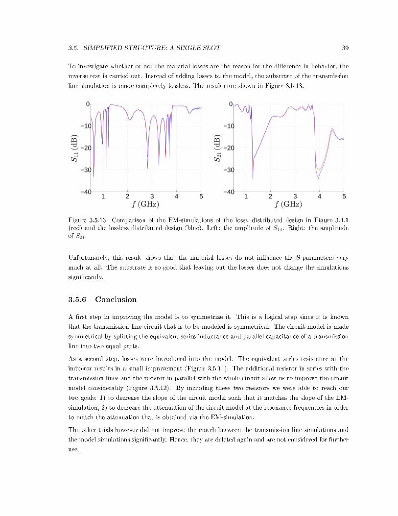
To investigate whether or not the material losses are the reason for the dierence in behavior, the
reverse test is carried out. Instead of adding losses to the model, the substrate of the transmission
line simulation is made completely lossless. The results are shown in Figure 3.5.13.
1 2 3 4 5−40
−30
−20
−10
0
f (GHz)
S11(dB)
1 2 3 4 5−40
−30
−20
−10
0
f (GHz)
S21(dB)
Figure 3.5.13: Comparison of the EM-simulations of the lossy distributed design in Figure 3.4.1(red) and the lossless distributed design (blue). Left: the amplitude of S11. Right: the amplitudeof S21.
Unfortunately, this result shows that the material losses do not inuence the S-parameters very
much at all. The substrate is so good that leaving out the losses does not change the simulations
signicantly.
3.5.6 Conclusion
A rst step in improving the model is to symmetrize it. This is a logical step since it is known
that the transmission line circuit that is to be modeled is symmetrical. The circuit model is made
symmetrical by splitting the equivalent series inductance and parallel capacitance of a transmission
line into two equal parts.
As a second step, losses were introduced into the model. The equivalent series resistance at the
inductor results in a small improvement (Figure 3.5.11). The additional resistor in series with the
transmission lines and the resistor in parallel with the whole circuit allow us to improve the circuit
model considerably (Figure 3.5.12). By including these two resistors we were able to reach our
two goals: 1) to decrease the slope of the circuit model such that it matches the slope of the EM-
simulation; 2) to decrease the attenuation of the circuit model at the resonance frequencies in order
to match the attenuation that is obtained via the EM-simulation.
The other trials however did not improve the match between the transmission line simulations and
the model simulations signicantly. Hence, they are deleted again and are not considered for further
use.
40 CHAPTER 3. MODELING A MICROSTRIP LINE WITH SLOTTED GROUND PLANE
Because we want to see how good the obtained, improved circuit model represents the transmission
line structure, we will t a model of a rational form on both the circuit model and the EM-simulations
in Section 3.6.
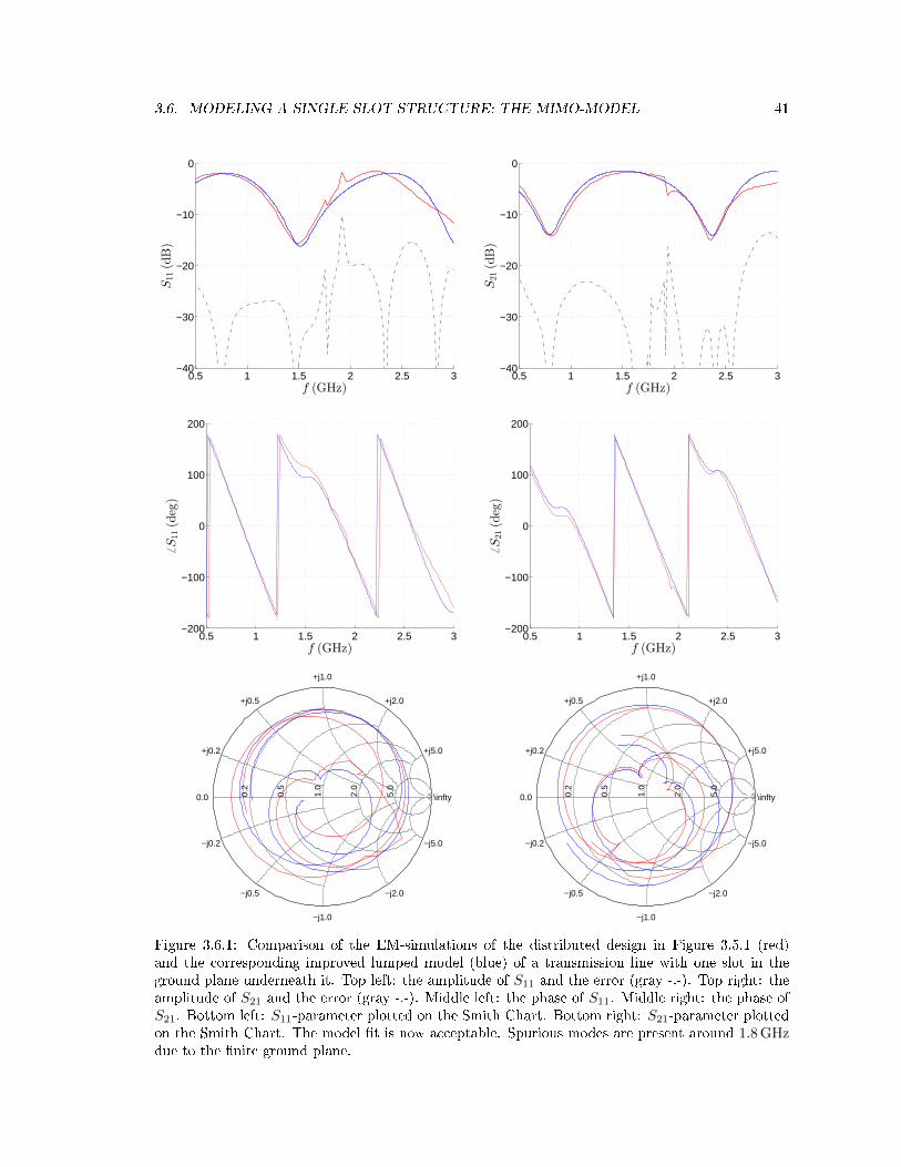
3.6 Modeling a single slot structure: the MIMO-model
In this section, a parametric MIMO-model is t to both the lumped-element circuit model and the
EM-simulations of a single slot structure. The model is a parametric MIMO-model with common
denominator. The selected MIMO-models for the lumped circuit model and the EM-simulations are
chosen to have the same order and their poles and zeros are compared.
3.6.1 Geometry and settings
The one-slot-structure that was used in Section 3.5 has a resonance frequency at 1.6 GHz. Hence, its
third resonance mode is already close to 5 GHz. Since we want to restrict the maximum simulation
frequency to 5 GHz at the most, we would like to decrease the rst resonance frequency of the
structure. We have seen before that increasing that length of the slotline(s) results in a decrease of
the resonance frequency. Therefore, a structure with a longer slotline is used in this section.
The geometry of the structure remains the same as in Section 3.5 (see Figure 3.5.1). The transmission
line has a characteristic impedance of 50 Ohm and a corresponding width of 3.4 mm. The width
of the slotline remains 5 mm, but the length is increased to 160 mm so that the rst resonance
frequency, calculated from Equation (3.3.7), is about 600 MHz. We select a frequency simulation
range from 500 MHz to 3 GHz with a frequency step of 20 MHz.
3.6.2 Improved lumped-element circuit model vs. EM-simulations
Figure 3.6.1 compares the improved circuit model (blue) to the EM-simulations (red). The real
resonance frequency is about 800 MHz instead of the expected frequency of 600 MHz. Note that this
frequency shift is already compensated in Figure 3.6.1.
An RMSE of about −22 dB and −23 dB was obtained for S11 and S21 respectively. That shows that
the improved model represents the transmission line structure very well. The match is good for the
amplitude as well as for the phase over the whole frequency band of interest. This is shown in the
top gures, where the error is plotted in gray (-.-), and the middle gures of Figure 3.6.1. The good
quality of the t is also clearly visible when the S-parameters are plotted on a Smith Chart (bottom
gures). Some spurious modes are present around 1.8 GHz in the EM-simulation. It is our belief
that they are devoted to the nite size of the ground plane.
3.6. MODELING A SINGLE SLOT STRUCTURE: THE MIMO-MODEL 41
0.5 1 1.5 2 2.5 3−40
−30
−20
−10
0
f (GHz)
S11(dB)
0.5 1 1.5 2 2.5 3−40
−30
−20
−10
0
f (GHz)
S21(dB)
0.5 1 1.5 2 2.5 3−200
−100
0
100
200
f (GHz)
6S11(deg)
0.5 1 1.5 2 2.5 3−200
−100
0
100
200
f (GHz)
6S21(deg)
0.2
0.5
1.0
2.0
5.0
+j0.2
−j0.2
+j0.5
−j0.5
+j1.0
−j1.0
+j2.0
−j2.0
+j5.0
−j5.0
0.0 \infty 0.2
0.5
1.0
2.0
5.0
+j0.2
−j0.2
+j0.5
−j0.5
+j1.0
−j1.0
+j2.0
−j2.0
+j5.0
−j5.0
0.0 \infty
Figure 3.6.1: Comparison of the EM-simulations of the distributed design in Figure 3.5.1 (red)and the corresponding improved lumped model (blue) of a transmission line with one slot in theground plane underneath it. Top left: the amplitude of S11 and the error (gray -.-). Top right: theamplitude of S21 and the error (gray -.-). Middle left: the phase of S11. Middle right: the phase ofS21. Bottom left: S11-parameter plotted on the Smith Chart. Bottom right: S21-parameter plottedon the Smith Chart. The model t is now acceptable. Spurious modes are present around 1.8 GHzdue to the nite ground plane.
42 CHAPTER 3. MODELING A MICROSTRIP LINE WITH SLOTTED GROUND PLANE
3.6.3 MIMO-model
In this section, we want to verify how good the improved lumped circuit model represents the EM-
simulations. To this end, we compare the position of the poles and zeros of both tted linear time-
invariant (LTI) models. We estimate a 2x2 parametric MIMO-model with a common denominator
starting from both the EM-simulation data and the lumped circuit model data. The Frequency
Domain Toolbox [14] is used for this purpose.
We start with the estimation of a common denominator MIMO-model using the EM-simulation data.
The parametric MIMO-model is estimated for the complete S-matrix of the lter. The available
simulation data represent the sampled S-parameter data of the lter, evaluated on a pre-specied
frequency grid. Only the simulation data that describe the rst resonance (range [0.5 GHz,1.5 GHz]
with a frequency step of 20 MHz) is used to estimate the MIMO-model, both in order to restrict the
model complexity and because the simulation data at higher frequencies may not prove to be very
accurate.
The simulated S-parameters, for which we want to estimate a MIMO-model, are evaluated on the
simulation frequency grid fi, 1 < i < N :
V ec(STEM (fi)) =
S11,EM (fi)
S12,EM (fi)
S21,EM (fi)
S22,EM (fi)
(3.6.1)
with SEM (fi) the S-matrix of the EM-simulation data.
The estimator requires an input signal to be useable, and this is set to a constant value to indicate
that an FRF is to be estimated.
The response of the system is then set to
V ec(STMIMO(fi)) =
S11,MIMO(fi)
S12,MIMO(fi)
S21,MIMO(fi)
S22,MIMO(fi)
with 1 < i < N and where SMIMO(fi) represents the parametric 2x2 MIMO-model of a rational
form of the S-matrix of the device under test (DUT).
The covariance matrix of these simulation data is chosen as in Equation (3.6.2) to impose a relative
error criterion on the model t.
3.6. MODELING A SINGLE SLOT STRUCTURE: THE MIMO-MODEL 43
Cov(SEM (fi)) =
1% |S11,EM (fi)|2 0 0 0
0 1% |S12,EM (fi)|2 0 0
0 0 1% |S21,EM (fi)|2 0
0 0 0 1% |S22,EM (fi)|2
(3.6.2)
In the Sampled Maximum Likelihood (SML) framework, Cov(SEM (fi)) represents the covariance
matrix of SEM (fi) with 1 < i < N . Note that the covariance matrix represents the simulation
error of ADS [3] since we are dealing with simulations and not with measurements. Therefore, this
quantity is extremely hard to get as it is almost impossible to force a dierent realization of the
noise. Since we do not have any information available about the correlation, we choose it to be zero.
The cost function is then dened as:
LK =
N∑i=1
eT (fi)Cov(SEM (fi)) e(fi)
with e(fi) = |V ec(SEM (fi))− V ec(SMIMO(fi))| the error to be minimized.
The SML estimator is used to estimate the parametric MIMO-model. The estimation and validation
process is not discussed in detail here since this is not our main focus and the measurement based
criteria do not really hold in this simulation context. For the full theoretical framework we refer to
[15].
The best model t is obtained for a model order [NB + 1 , NA + 1] of [5, 5], with NB the number of
zeros and NA the number of poles. Figure 3.6.2 and 3.6.3 respectively show the t of the amplitude
and phase of the S-parameters of the MIMO-model (full blue line) to the EM-simulation data (full
red line). The user selected standard deviation of the EM-simulated FRFs (1 % relative error)
(dashed blue line) is compared to the obtained model error (dashed gray line (-.-)) to assess the
quality of the estimated model.
Even if the simulation of the transmission line structure were perfect, the presence of this model
error is expected. We t a model of a rational form to the transcendental simulation data and
clearly these functions do not behave equally. However, the simulation data actually represent a
meromorphic function. Since the simulation frequency band is nite, the meromorphic transcen-
dental function can be approximated with an arbitrary precision by a rational form of nite order
[16]. This approximation error will decrease if the model order of the rational function is increased.
However, increasing the model order will also increase the model complexity and the model might
become unstable. Hence, a good balance between the model variability (model order) and the model
complexity is needed and is obtained here for an order of [5, 5].
To get a better idea of the average level of the model error, the RMS-value of the model error is
calculated for each S-parameter:
44 CHAPTER 3. MODELING A MICROSTRIP LINE WITH SLOTTED GROUND PLANE
RMSE =
[RMSES11 RMSES12
RMSES21 RMSES22
]=
[−29 −31
−31 −28
]dB
The RMSE-values are similar to the level of the user selected standard deviation of the to be modeled
FRFs (Equation (3.6.2)). Based on this knowledge we may assume there is a good balance between
the model complexity and the model variability.
0.4 0.6 0.8 1 1.2−60
−45
−30
−15
0
f (GHz)
S11(dB)
0.4 0.6 0.8 1 1.2−60
−45
−30
−15
0
f (GHz)
S12(dB)
0.4 0.6 0.8 1 1.2−60
−45
−30
−15
0
f (GHz)
S21(dB)
0.4 0.6 0.8 1 1.2−60
−45
−30
−15
0
f (GHz)
S22(dB)
Figure 3.6.2: Comparison of the amplitudes of the parametric MIMO-model (blue) and the EM-simulation data (red) and comparison of the user selected standard deviation (Equation (3.6.2)) ofthe EM-simulation data (dashed blue) and the model error (gray -.-). Top left: S11. Top right: S12.Bottom left: S21. Bottom right: S22.
Note that the S11- and the S22-parameter of the EM-simulations are not perfectly equal (this is
clearly noticeable when looking at the RMSE values). This implies that the structure is asymmetri-
cal. However, we know that the transmission line structure modeled here is perfectly symmetrical.
3.6. MODELING A SINGLE SLOT STRUCTURE: THE MIMO-MODEL 45
The small deviation between S11 and S22 can therefore only be attributed to simulation inaccuracies
of ADS [3].
0.4 0.6 0.8 1 1.2−500
−400
−300
−200
−100
f (GHz)
6S11(deg)
0.4 0.6 0.8 1 1.2−200
−100
0
100
200
f (GHz)
6S12(deg)
0.4 0.6 0.8 1 1.2−200
−100
0
100
200
f (GHz)
6S21(deg)
0.4 0.6 0.8 1 1.2−500
−400
−300
−200
−100
f (GHz)
6S22(deg)
Figure 3.6.3: Comparison of the phases of the parametric MIMO-model (blue) and the EM-simulation data (red). Top left: S11. Top right: S12. Bottom left: S21. Bottom right: S22.
In a second step, a common denominator MIMO-model is t to S-matrix of the lumped-element
circuit model data evaluated on the same frequency grid. The input and output matrices and their
sample noise covariances are again dened as in Equations (3.6.1) and (3.6.2).
We now want to compare the S-matrix response of the estimated MIMO-model to the one that was
t on the EM-simulations. Therefore, the model order is chosen to be the same as for the EM-based
MIMO-model, namely [5, 5].
Figure 3.6.4 and 3.6.5 respectively show the t of the amplitude and the phase of the S-parameters
of the MIMO-model (full blue line) to the lumped model data (full red line).
46 CHAPTER 3. MODELING A MICROSTRIP LINE WITH SLOTTED GROUND PLANE
The user selected standard deviation of the FRFs of the lumped circuit model (dashed blue line)
is again compared to the model error (dashed gray line (-.-)) to assess the quality of the estimated
model. The RMS-values of the model error are similar to the level of the user selected standard
deviation (Equation (3.6.2)):
RMSE =
[RMSES11
RMSES12
RMSES21RMSES22
]=
[−28 −32
−32 −28
]dB
Again, a good balance exists between the model complexity and the model variability.
0.4 0.6 0.8 1 1.2−60
−45
−30
−15
0
f (GHz)
S11(dB)
0.4 0.6 0.8 1 1.2−60
−45
−30
−15
0
f (GHz)
S12(dB)
0.4 0.6 0.8 1 1.2−60
−45
−30
−15
0
f (GHz)
S21(dB)
0.4 0.6 0.8 1 1.2−60
−45
−30
−15
0
f (GHz)
S22(dB)
Figure 3.6.4: Comparison of the amplitudes of the parametric MIMO-model (blue) and the lumpedmodel data (red) and comparison of the user selected standard deviation of the FRFs of the lumpedmodel (dashed blue) and the model error (gray -.-). Top left: S11. Top right: S12. Bottom left:S21. Bottom right: S22.
Note that the S11- and the S22-parameter of the lumped model are indeed perfectly equal. This is
3.6. MODELING A SINGLE SLOT STRUCTURE: THE MIMO-MODEL 47
as expected since the lumped model was made symmetrical in Section 3.5.4.
0.4 0.6 0.8 1 1.2−500
−400
−300
−200
−100
f (GHz)
6S11(deg)
0.4 0.6 0.8 1 1.2−200
−100
0
100
200
f (GHz)
6S12(deg)
0.4 0.6 0.8 1 1.2−200
−100
0
100
200
f (GHz)
6S21(deg)
0.4 0.6 0.8 1 1.2−500
−400
−300
−200
−100
f (GHz)
6S22(deg)
Figure 3.6.5: Comparison of the phases of the parametric MIMO-model (blue) and the lumpedmodel data (red). Top left: S11. Top right: S12. Bottom left: S21. Bottom right: S22.
Let us rst introduce some names for simplicity.
EM MIMO-model: the parametric MIMO-model that is estimated on the EM-simulation data
circuit MIMO-model: the parametric MIMO-model that is estimated on the lumped circuit
model data
Figure 3.6.6 compares the poles and zeros of EM MIMO-model (red) and circuit MIMO-model
(blue). All S-parameters have the same poles, since the MIMO-model is a common denominator
model. Note that the imaginary axis is scaled by 2π to convert the angular frequency ω = 2πf into
frequency f . Remark that the MIMO-models are both stable. The dashed blue lines indicate the
frequency range for which the model is extracted.
48 CHAPTER 3. MODELING A MICROSTRIP LINE WITH SLOTTED GROUND PLANE
0 5 10 15
x 109
−5
0
5
x 109
−1 0 1 2
x 109
−1
−0.5
0
0.5
1
x 109
−1 0 1 2
x 109
−1
−0.5
0
0.5
1
x 109
0 5 10 15
x 109
−5
0
5
x 109
Figure 3.6.6: Comparison of the the poles and zeros of the parametric MIMO-model estimated onthe EM-simulation data (red) and the parametric MIMO-model estimated on the lumped modeldata (blue). The dashed blue lines indicate the frequency range of operation. Top left: S11. Topright: S12. Bottom left: S21. Bottom right: S22.
Tables 3.3 and 3.4 give the relative deviations, ξ, between the poles and zeroes of the two MIMO-
models respectively. The errors of the real and imaginary part are evaluated separately. The relative
error for e.g. the real part of a pole is calculated as follows:∣∣∣∣Re(pole of the EM MIMO model)− Re(pole the circuit MIMO model)
Re(pole of the EM MIMO model)
∣∣∣∣
3.6. MODELING A SINGLE SLOT STRUCTURE: THE MIMO-MODEL 49
Table 3.3: Relative errors, ξ, of the real, Re, and imaginary part, Im, of the poles of EM MIMO-model and circuit MIMO-model. Since it is a common denominator model, all S-parameters havethe same pole pairs (PP).
PP 1 PP 2ξ(Re) (%) 9.6 0.25ξ(Im) (%) 0.89 3.0
The real part of the pole pair (PP) 1 shows a deviation of about 10 %, which is very high, and
explains the dierence in damping present in the FRFs. The PP 1 of EM MIMO-model is located
at a larger distance from the imaginary axis than PP 1 of circuit MIMO-model. This means that
the quality factor of circuit MIMO-model is still 10 % higher than the one of EM MIMO-model.
We can conclude that the quality factor of the poles in the EM-simulation is still not modeled well
enough by the lumped-element circuit model.
The deviation of the real part of the zero pair (ZP) 1 of the S12 and S21-parameters is quite high.
Note that the match of ZP 1 of S22 is much better than the match of ZP 1 of S11. We expect
a similar match would for both since the structure is symmetric, but this is not the case due to
simulations inaccuracies of ADS [3].
The other PPs and ZPs show a very good match. Remark that the errors of the imaginary parts
of all PPs and ZPs are acceptable. This is a good thing since the imaginary part is related to the
frequency of the poles and zeros. We can conclude that the frequencies at which the poles and zeros
are located show a very good match between the two MIMO-models.
Table 3.4: Relative errors of the real and imaginary part of the poles of EM MIMO-model andcircuit MIMO-model. Parameter S12 and S21 have the same zero pairs (ZP) because the circuit issymmetric. The ZPs of S11 and S22 of EMMIMO-model slightly dier due to simulation inaccuraciesof ADS [3].
Note that the remaining zeros of S11 and S22 are not discussed yet. We see that these zeros are
completely dierent for the two MIMO-models. This is not a very big problem since we know
that positive real zeros, called minimum phase zeros, are necessary to make the phase delay, that is
present in Figures 3.6.3 and 3.6.5, possible. The fact that these zeros dier for the two MIMO-models
is not a problem since we could make these zeros disappear by doing a phase correction.
3.6.4 Conclusion
We conclude that the improved lumped-element circuit model matches the EM-simulations quite
well. The level of agreement is shown by estimating a parametric MIMO-model using the EM-
50 CHAPTER 3. MODELING A MICROSTRIP LINE WITH SLOTTED GROUND PLANE
simulation data and the lumped circuit model data and comparing the obtained poles and zeros.
The poles of the lumped-element circuit model do indeed match the poles of the EM-simulation data.
Hence, the circuit model captures the essence of the behavior of the transmission line structure.
An important disadvantage is that the quality factor of the poles and zeros is still not modeled very
well. To improve on the modeling of the quality factor, the element(s) of the circuit that create
this damping should be located. Next, we should check whether it is possible to adjust the element
values of the losses to improve the modeling of the quality factor.
3.7 Conclusion
It was shown in this chapter that the transmission line structure with slotted ground plane behaves
as a bandstop lter. Hence, this structure can be used to attenuate the harmonic responses in lter
design. An extra benet is that we can choose up to some level which harmonics we want to excite
simply by the selecting the position of the feedpoint of the slot(s).
A lumped element circuit model was generated that is symmetric and able to accurately predict the
quality factors and anti-resonances of the transmission line structure. Hence, this lumped model is
a very important step towards a proper lter design with slotted ground plane.
Chapter 4
Coupled line with slotted ground
plane
4.1 Introduction
In Chapter 3, we examined a transmission line with a periodic repetition of slots in the ground
plane underneath it. The next step is to examine the use of this slotted ground plane structure in
combination with a coupled line in an attempt to use it in lter design later on. Since introducing
a coupled line results in the introduction of an extra coupling next to the coupling to the slots
and changes the eld pattern quite extensively, there is an extra complication in the simulation.
It is possible that the EM-simulator of ADS [3] is not really capable anymore to simulate the real
behavior of this more complex structure correctly and accurately enough for our modeling purposes.
Therefore this chapter is devoted to the verication of the correctness of the EM-simulations for
coupled line structures with slotted ground plane.
Section 4.2 describes the geometry of the coupled line structure itself. Section 4.3 compares the
simulations and the measurements of three dierent coupled line structures. The three structures
are selected to show dierent steps in the validation process. First, a structure without any slots is
realized as a reference element. Next, a coupled line with one slot is used to see and understand the
inuence of the slot coupling on the line coupling. Finally, a structure with three slots is realized
to represent a practically useable lter. Section 4.4 discusses the eects of the slots in the ground
plane underneath the coupled line.
51
52 CHAPTER 4. COUPLED LINE WITH SLOTTED GROUND PLANE
4.2 Geometry and settings
A simple coupled line structure is designed as shown in Figure 4.2.1. The microstrip lines have a
width W = 3.4 mm corresponding to a characteristic impedance of 50 Ohm. The lines are coupled
over λ/2 and the resonance wavelength, λ, is selected to correspond to a resonance frequency of
1 GHz. This yields λ ≈ 176 mm for the considered substrate (see Section 2.3). The spacing between
the lines, S1, is set to 1.5 mm. Hereby, the spacing is small enough so that coupling between the
lines occurs, but not too small to make sure the design can still be fabricated accurately and a
potential increase in the coupling between the lines can easily be noticed.
Three dierent designs of similar structures are realized: one without any slots, one with only one
slot and one with three slots in the ground plane. Figure 4.2.1 only shows the structure with one
slot. The other two are similar and the slots are always arranged symmetrically with respect to
the coupled line section.. The approach explained in Chapter 3 is used to design the dimensions.
The slots have a width Ws = 5 mm, which corresponds to a characteristic impedance of the slotline
of Zslot0 ≈ 14e1 Ohm. The length of the slotlines is d = 60 mm, which corresponds to a resonance
frequency of f1 ≈ 1.7 GHz. The length of a unit cell is p = 8 mm. The slots have two feedpoints
that are positioned symmetrically with respect to the lines in both directions.
Figure 4.2.1: Coupled line structure with slots in the ground plane underneath it. The slots havetwo feedpoints that are arranged symmetrically with respect to the lines. The spacing between thelines is S1. The length of the coupled lines is λ
4 . The slots have a width Ws = 5 mm and a lengthd = 60 mm. The length of a unit cell is p = 8 mm.
The structures are simulated over a frequency range of 100 MHz to 3 GHz with a frequency step of
20 MHz. For the settings of the EM-simulator is referred to Chapter 2.
4.3. COMPARING EM-SIMULATIONS TO MEASUREMENTS 53
4.3 Comparing EM-simulations to measurements
Figure 4.3.1 compares the EM-simulations (red) to the measurements (green) of the structure with-
out slots in the ground plane, as described in Section 4.2. Since no slots are present, we expect that
the simulations predict the real behavior very well because this type of line is one of the classical
structures simulated with ADS [3].
0.5 1 1.5 2 2.5 3−1
−0.8
−0.6
−0.4
−0.2
0
f (GHz)
S11(dB)
0.5 1 1.5 2 2.5 3−60
−50
−40
−30
−20
−10
f (GHz)
S21(dB)
0.5 1 1.5 2 2.5 3−200
−100
0
100
200
f (GHz)
6S11(deg)
0.5 1 1.5 2 2.5 3−200
−100
0
100
200
f (GHz)
6S21(deg)
Figure 4.3.1: Comparison of the EM-simulations (red) and the measurements (green) of the coupledline structure, introduced in Figure 4.2.1, without slots. Top left: the amplitude of S11. Top right:the amplitude of S21 and the error (gray -.-). Bottom left: the phase of S11. Bottom right: thephase of S21. The EM-simulations match the measurements very well.
As expected, the EM-simulations predict the real behavior of the structure very well. This is proven
by looking at the value of the RMSE. An RMSE of about −32 dB and −39 dB is obtained over the
frequency band of interest for S11 and S21 respectively. The magnitude of the squared complex
dierence (gray -.-) between the simulation and the measurement of S21 is shown in Figure 4.3.1
54 CHAPTER 4. COUPLED LINE WITH SLOTTED GROUND PLANE
(top right). For S11 the error is not shown since the overall error is about 30 % lower than S11,
relative to the amplitude of S11 (see RMSE-value of S11 given previously). The ripples in the
error are explained as follows. The measured data have an irrational form. The EM-simulation is
an approximation for this irrational form. Therefore, the simulated data are wrapped around the
measured data, resulting in ripples.
A small dierence in time delay is present between the simulations and the measurements. This can
be explained by the approximation that is used by ADS [3] to calculate the eective permittivity
and the position of the reference plane of the calibration of the VNA. An intermediate connection
piece with a length of about 0.5 mm was present during the measurements that is not accounted for
in the measurement data that are shown. At 3 GHz this length corresponds to a delay of about 30°,
which is consistent with the delay that is present in Figure 4.3.1 .
Figure 4.3.2 and Figure 4.3.3 compare the EM-simulations (red) to the measurements (green) of the
coupled line structure with respectively one slot and three slots in the ground plane.
The error (gray -.-) is shown on the amplitude plots of S11 (top left) and S21 (top right) on Figures
4.3.2 and 4.3.3. The ripples in the error are again explained by the fact that the simulated data are
wrapped around the measured data.
4.3. COMPARING EM-SIMULATIONS TO MEASUREMENTS 55
0.5 1 1.5 2 2.5 3−60
−45
−30
−15
0
f (GHz)
S11(dB)
0.5 1 1.5 2 2.5 3−60
−45
−30
−15
0
f (GHz)
S21(dB)
0.5 1 1.5 2 2.5 3−200
−100
0
100
200
f (GHz)
6S11(deg)
0.5 1 1.5 2 2.5 3−200
−100
0
100
200
f (GHz)
6S21(deg)
Figure 4.3.2: Comparison of the EM-simulations (red) and the measurements (green) of the coupledline structure, introduced in Figure 4.2.1, with one slot. Top left: the amplitude of S11 and theerror (gray -.-). Top right: the amplitude of S21 and the error (gray -.-). Bottom left: the phase ofS11. Bottom right: the phase of S21. The EM-simulations match the measurements very well.
The obtained RMS-values for the two structures are given in Table 4.1. For the structure with three
slots, the RMS-values for S11 and S21 are higher than for the one-slot structure. This is due to the
high error peak that is present in the three-slot structure (Figure 4.3.3) around 1.5 GHz. This error
peak is present due to a small shift in the resonance frequency between the EM-simulations and
the measurements around 1.5 GHz. This peak pushes the RMSE to higher values as what can be
expected.
Table 4.1: RMSE values for the coupled line structures with 1 and 3 slots.
1 slot 3 slotsS11 −28 dB −27 dBS21 −32 dB −25 dB
56 CHAPTER 4. COUPLED LINE WITH SLOTTED GROUND PLANE
0.5 1 1.5 2 2.5 3−60
−45
−30
−15
0
f (GHz)
S11(dB)
0.5 1 1.5 2 2.5 3−60
−45
−30
−15
0
f (GHz)
S21(dB)
0.5 1 1.5 2 2.5 3−200
−100
0
100
200
f (GHz)
6S11(deg)
0.5 1 1.5 2 2.5 3−200
−100
0
100
200
f (GHz)
6S21(deg)
Figure 4.3.3: Comparison of the EM-simulations (red) and the measurements (green) of the coupledline structure, introduced in Figure 4.2.1, with three slots. Top left: the amplitude of S11 and theerror (gray -.-). Top right: the amplitude of S21 and the error (gray -.-). Bottom left: the phase ofS11. Bottom right: the phase of S21. The EM-simulations match the measurements very well.
Both EM-simulations show a good prediction of the real behavior of the structure. The simulated
resonances are clearly present in the measurements and all the measured resonances are predicted by
the EM-simulator. This clearly shows that the EM-simulator may be used in a real design context.
The match of the phases is also very good, except for a small dierence in time delay due to
the calibration plane of the VNA and the approximation of the eective permittivity in ADS [3].
However, this dierence was also present in the design without slots. This means this delay dierence
is not related to the slots but has the same origin as in the design with the full ground plane.
4.4. EFFECT OF THE SLOTS 57
4.4 Eect of the slots
Comparing Figures 4.3.1, 4.3.2 and 4.3.3 shows the eect of introducing one or more slots in the
ground plane underneath a coupled line.
First of all, the maximum forward transmission, S21, of the structure without slots (Figure 4.3.1)
reaches more or less −10 dB. This is much lower than the maximum of S21 of the structure with
one or three slots, where S21 arrives at almost 0 dB. This means that introducing slots underneath
the coupled line increases the coupling between the lines signicantly.
This is an advantage that we can try to exploit for lter design. In wideband lters a strong coupling
is required between the coupled lines. To achieve a strong coupling in a classical coupled line setting,
the gap between the lines is decreased accordingly. However, decreasing the dimensions is limited
by the accuracy of the production process. The strength of the coupling of the lines is therefore also
limited. This is where introducing slots in the ground plane can bring a solution. As they allow to
increase the coupling of the lines without having to push the dimensions of the structure to their
lower limit, they can pave the way to broadband designs with low insertion losses.
Explaining the eect of the slots on the shape of the amplitudes of S11 and S21 is not straight-
forward. Further research on the modeling of these eects is necessary to come up with a design
procedure.
4.5 Conclusion
We can conclude that the EM-simulation of a coupled line structure with slots in the ground plane
is very reliable. This is a big advantage if we want to use these kind of structures for lter design
procedures.
An advantage of introducing slots in the ground plane of a coupled line is that the slots can increase
the coupling between the line. In lter design, this can be of great benet to increase the bandwidth
of the lters keeping the insertion losses low and without having to decrease the dimensions of the
lter signicantly. The interpretation of the overall eects of the slots on the coupled line is not
straight-forward and requires further research.
Chapter 5
Conclusion and future perspectives
The aim of this thesis is to examine the use of slots in the ground plane of coupled microstrip line
lters and to investigate their use in practical lter design procedures, hereby working towards the
design of wideband lters with low insertion losses. This research yields ve main results.
In the rst part of the thesis we examine and adapt the settings of the EM-simulator that are required
to accurately simulate a nite ground plane. The validity of the settings that are required to properly
simulate a slotted ground plane is veried by comparing the EM-simulations to the measurements
of the realized designs. We show that the EM-simulator is indeed capable of simulating defective
ground plane structures accurately.
Secondly, we examine a simple microstrip line with a slotted ground plane. Simulations and mea-
surements that this structure behaves as a bandstop lter. This eect can be used in lter design
to attenuate the spurious harmonic responses that are present in the classical parallel-coupled line
lters. Moreover, the position of the feedpoint of the slots can be used to select, up to some level,
which harmonics are attenuated and which are not.
Next, we investigate an existing lumped-element equivalent circuit model that should predict the
behavior of the slots. The original lumped circuit model is not accurate enough to be used in
practical design purposes. We propose several improvements to the original lumped circuit model
that remediate its shortcomings. First of all the improved lumped model is made symmetric. This
is necessary because the transmission line structure is also clearly symmetric by nature. Secondly,
the model is adapted to better predict the quality factor and the anti-resonances.
A parametric MIMO-LTI-model is estimated next starting from the EM-simulations and the lumped
circuit model response to verify how accurately the improved model can predict the behavior of the
transmission line structure. Comparing the poles and zeros shows a very good agreement indeed. It
is shown that the resonance frequency of the poles and zeros is predicted accurately. Some additional
improvement is still needed to predict the quality factor of the transmission line structure with very
high precision.
59
60 CHAPTER 5. CONCLUSION AND FUTURE PERSPECTIVES
Finally, a simple coupled line structure with slotted ground plane is analyzed. It is shown that
introducing slots in the ground plane indeed increases the coupling between the lines. This can be
of great benet when used in broadband lter design, since it allows to increase the bandwidth of
the lters while keeping the insertion loss low and without having to increase the dimensions of the
lters signicantly.
We can conclude that there is a lot of potential in the use of defective ground planes in lter design.
It is shown that introducing slots in the ground plane can solve the two main shortcomings of the
classical parallel-coupled transmission-line-resonator lters developed by Cohn [1]. Further research
is needed to include this properly in a lter design procedure.
Although this thesis is especially targeted to the use of a slotted ground plane in classical coupled-
line lter design. Defective ground planes can also be of great use in the design of hairpin resonator
lters, patch antennas and possible for dierent applications. There is still a lot of research potential
in dierent aspects of this subject.
Bibliography
[1] S. B. Cohn, Parallel-coupled transmission-line-resonator lters, Microwave Theory and Tech-
niques, IRE Transactions on, vol. 6, no. 2, pp. 223231, April 1958.
[2] Agilent Technologies, Momentum - the leading 3D planar EM simulator, 2013. [Online].