26
Modeling Digital Systems with VHDL Reference: Roth & John text – Chapter 2 Michael Smith text – Chapters 8 & 10
Modeling Digital Systems with VHDL
Reference: Roth & John text – Chapter 2Michael Smith text – Chapters 8 & 10
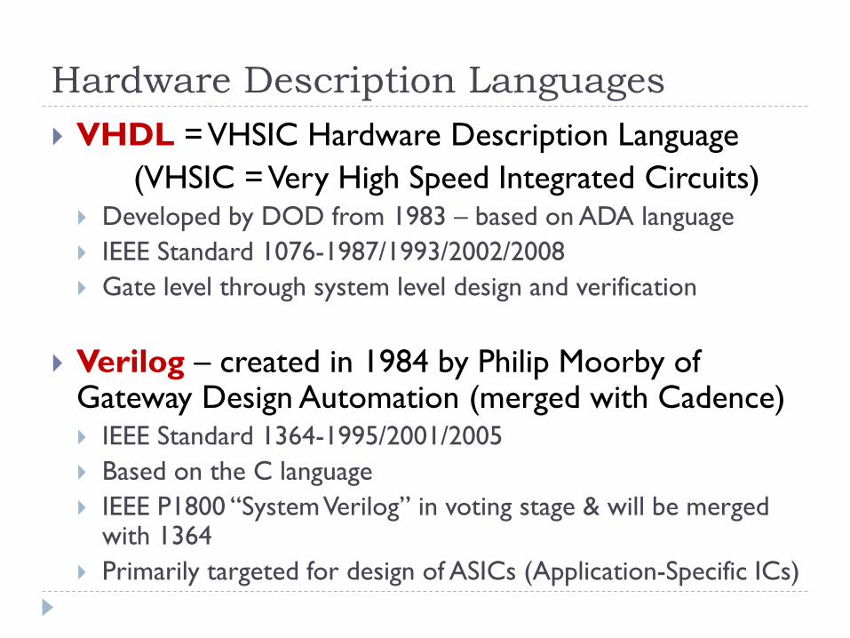
Hardware Description Languages VHDL = VHSIC Hardware Description Language
(VHSIC = Very High Speed Integrated Circuits) Developed by DOD from 1983 – based on ADA language IEEE Standard 1076-1987/1993/2002/2008 Gate level through system level design and verification
Verilog – created in 1984 by Philip Moorby of Gateway Design Automation (merged with Cadence) IEEE Standard 1364-1995/2001/2005 Based on the C language IEEE P1800 “System Verilog” in voting stage & will be merged
with 1364 Primarily targeted for design of ASICs (Application-Specific ICs)
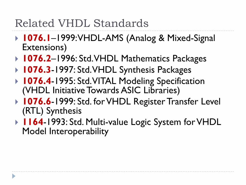
Related VHDL Standards 1076.1–1999: VHDL-AMS (Analog & Mixed-Signal
Extensions) 1076.2–1996: Std. VHDL Mathematics Packages 1076.3-1997: Std. VHDL Synthesis Packages 1076.4-1995: Std. VITAL Modeling Specification
(VHDL Initiative Towards ASIC Libraries) 1076.6-1999: Std. for VHDL Register Transfer Level
(RTL) Synthesis 1164-1993: Std. Multi-value Logic System for VHDL
Model Interoperability
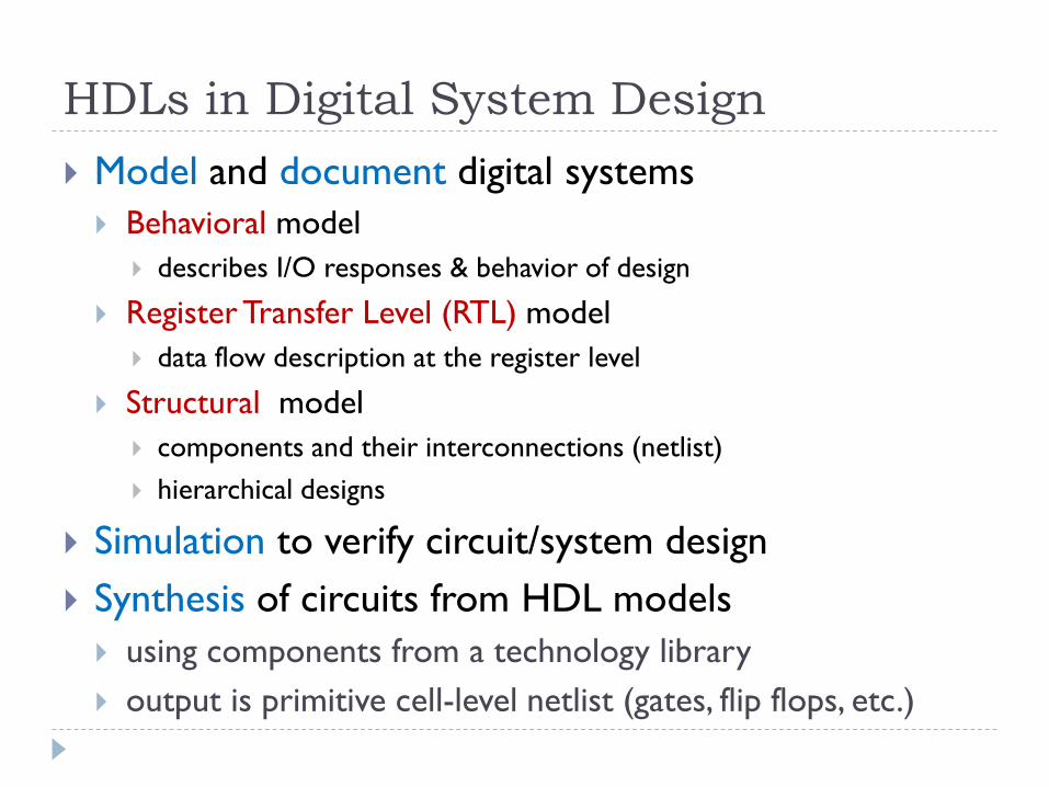
HDLs in Digital System Design Model and document digital systems Behavioral model
describes I/O responses & behavior of design
Register Transfer Level (RTL) model data flow description at the register level
Structural model components and their interconnections (netlist) hierarchical designs
Simulation to verify circuit/system design Synthesis of circuits from HDL models using components from a technology library output is primitive cell-level netlist (gates, flip flops, etc.)
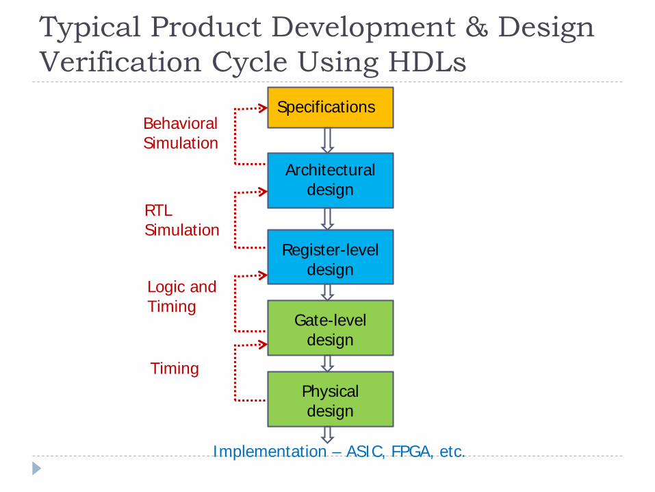
Typical Product Development & Design Verification Cycle Using HDLs
Specifications
Architecturaldesign
Register-leveldesign
Gate-leveldesign
Physical design
BehavioralSimulation
RTLSimulation
Logic andTiming
Timing
Implementation – ASIC, FPGA, etc.
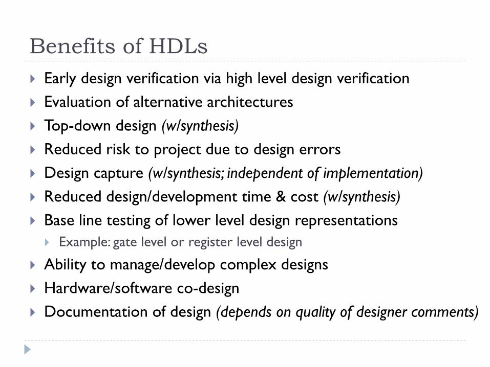
Benefits of HDLs Early design verification via high level design verification Evaluation of alternative architectures Top-down design (w/synthesis) Reduced risk to project due to design errors Design capture (w/synthesis; independent of implementation) Reduced design/development time & cost (w/synthesis) Base line testing of lower level design representations Example: gate level or register level design
Ability to manage/develop complex designs Hardware/software co-design Documentation of design (depends on quality of designer comments)
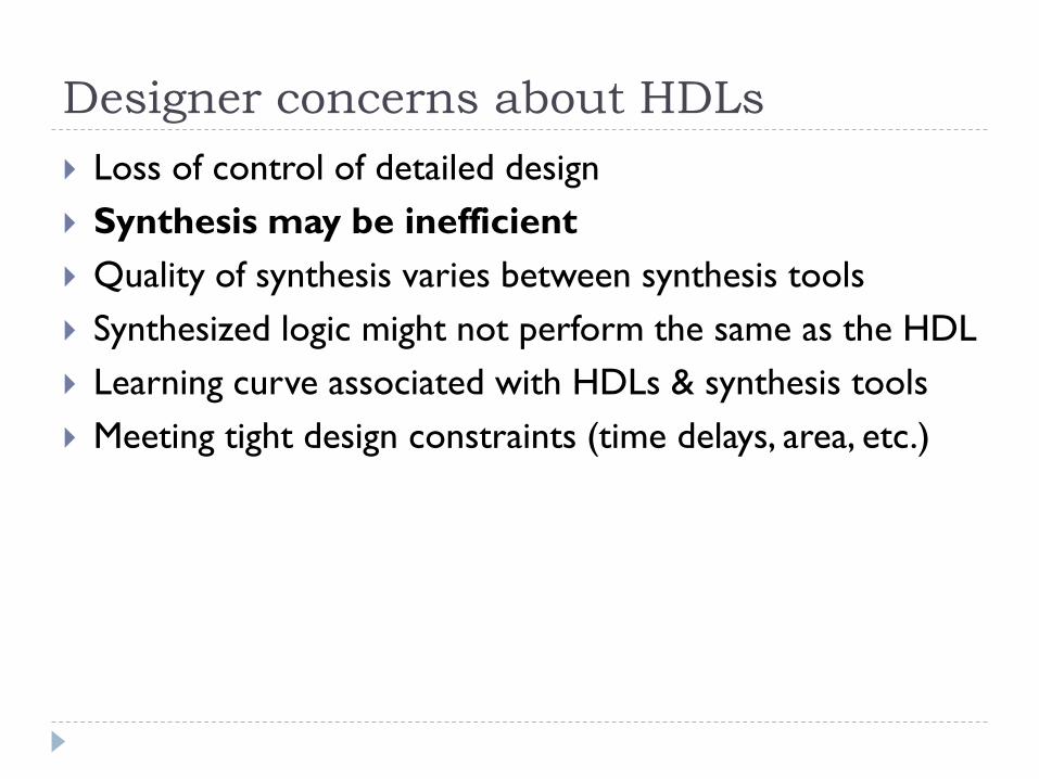
Designer concerns about HDLs Loss of control of detailed design Synthesis may be inefficient Quality of synthesis varies between synthesis tools Synthesized logic might not perform the same as the HDL Learning curve associated with HDLs & synthesis tools Meeting tight design constraints (time delays, area, etc.)
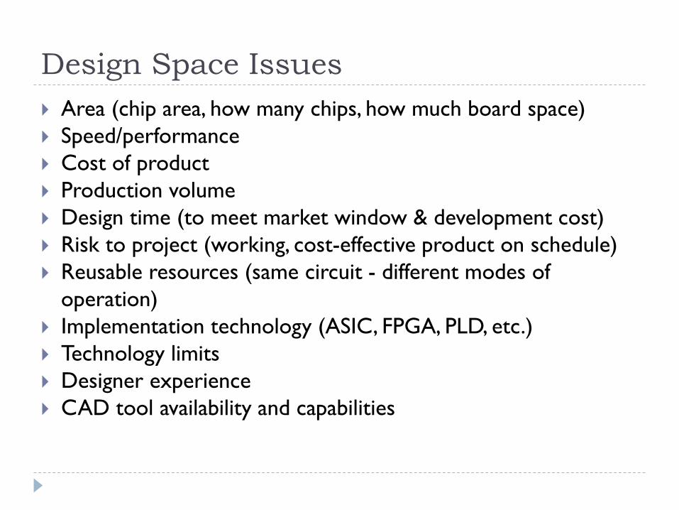
Design Space Issues Area (chip area, how many chips, how much board space) Speed/performance Cost of product Production volume Design time (to meet market window & development cost) Risk to project (working, cost-effective product on schedule) Reusable resources (same circuit - different modes of
operation) Implementation technology (ASIC, FPGA, PLD, etc.) Technology limits Designer experience CAD tool availability and capabilities
DoD requirements on VHDL in mid 80s: Design & description of hardware Simulation & documentation (with designer comments) Design verification & testing Concurrency to accurately reflect behavior & operation of
hardware (all hardware operates concurrently) as a result, all VHDL simulation is event-driven
Hierarchical design – essential for efficient, low-risk design Library support – for reuse of previously verified components Generic design - independent of implementation media Optimize - for area and/or performance Timing control – to assign delays for more accurate simulation Portability between simulators & synthesis tools (not always true)
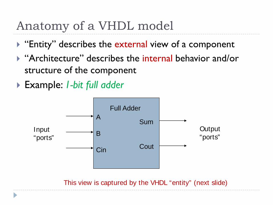
Anatomy of a VHDL model “Entity” describes the external view of a component “Architecture” describes the internal behavior and/or
structure of the component
Example: 1-bit full adder
A
B
Cin
Sum
Cout
Full Adder
Input“ports”
Output“ports”
This view is captured by the VHDL “entity” (next slide)
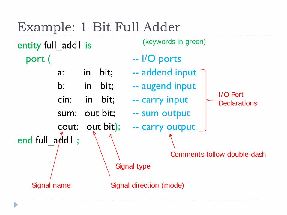
Example: 1-Bit Full Adderentity full_add1 is
port ( -- I/O portsa: in bit; -- addend inputb: in bit; -- augend inputcin: in bit; -- carry inputsum: out bit; -- sum outputcout: out bit); -- carry output
end full_add1 ;Comments follow double-dash
Signal type
Signal direction (mode)Signal name
I/O PortDeclarations
(keywords in green)
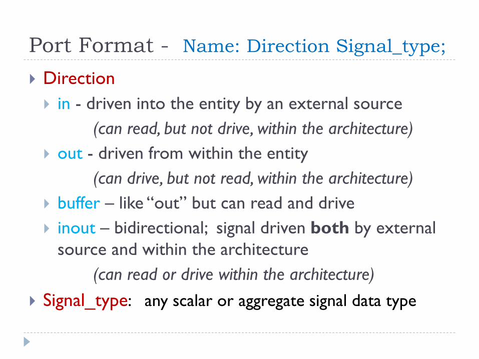
Port Format - Name: Direction Signal_type;
Direction in - driven into the entity by an external source
(can read, but not drive, within the architecture) out - driven from within the entity
(can drive, but not read, within the architecture) buffer – like “out” but can read and drive inout – bidirectional; signal driven both by external
source and within the architecture (can read or drive within the architecture)
Signal_type: any scalar or aggregate signal data type
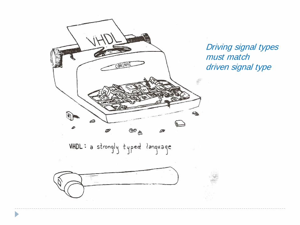
Driving signal typesmust match driven signal type
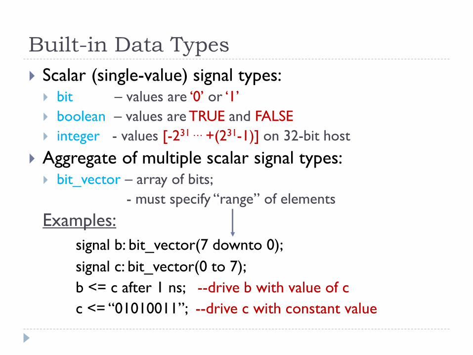
Built-in Data Types Scalar (single-value) signal types: bit – values are ‘0’ or ‘1’ boolean – values are TRUE and FALSE integer - values [-231 … +(231-1)] on 32-bit host
Aggregate of multiple scalar signal types: bit_vector – array of bits;
- must specify “range” of elementsExamples:
signal b: bit_vector(7 downto 0);signal c: bit_vector(0 to 7);b <= c after 1 ns; --drive b with value of cc <= “01010011”; --drive c with constant value
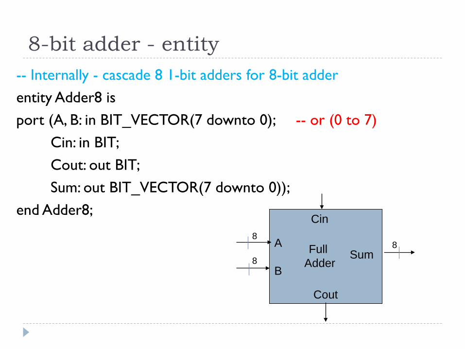
8-bit adder - entity-- Internally - cascade 8 1-bit adders for 8-bit adderentity Adder8 is port (A, B: in BIT_VECTOR(7 downto 0); -- or (0 to 7)
Cin: in BIT; Cout: out BIT; Sum: out BIT_VECTOR(7 downto 0));
end Adder8;
A
BSumFull
Adder
Cout
Cin
8
88
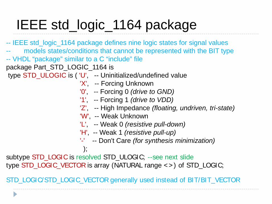
-- IEEE std_logic_1164 package defines nine logic states for signal values-- models states/conditions that cannot be represented with the BIT type-- VHDL “package” similar to a C “include” file package Part_STD_LOGIC_1164 istype STD_ULOGIC is ( 'U', -- Uninitialized/undefined value
'X', -- Forcing Unknown'0', -- Forcing 0 (drive to GND)'1', -- Forcing 1 (drive to VDD)'Z', -- High Impedance (floating, undriven, tri-state)'W', -- Weak Unknown'L', -- Weak 0 (resistive pull-down)'H', -- Weak 1 (resistive pull-up)'-' -- Don't Care (for synthesis minimization));
subtype STD_LOGIC is resolved STD_ULOGIC; --see next slidetype STD_LOGIC_VECTOR is array (NATURAL range <>) of STD_LOGIC;
STD_LOGIC/STD_LOGIC_VECTOR generally used instead of BIT/BIT_VECTOR
IEEE std_logic_1164 package
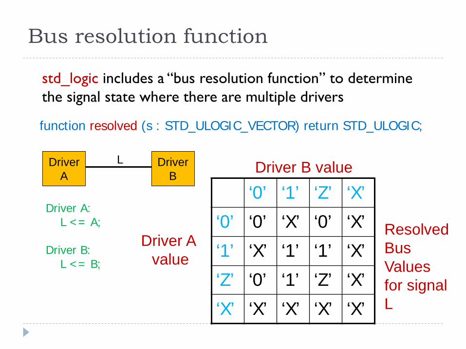
Bus resolution function
std_logic includes a “bus resolution function” to determine the signal state where there are multiple drivers
‘0’ ‘1’ ‘Z’ ‘X’
‘0’ ‘0’ ‘X’ ‘0’ ‘X’
‘1’ ‘X’ ‘1’ ‘1’ ‘X’
‘Z’ ‘0’ ‘1’ ‘Z’ ‘X’
‘X’ ‘X’ ‘X’ ‘X’ ‘X’
DriverA
DriverB Driver B value
Driver A value
ResolvedBusValues for signalL
function resolved (s : STD_ULOGIC_VECTOR) return STD_ULOGIC;
Driver A:L <= A;
Driver B:L <= B;
L
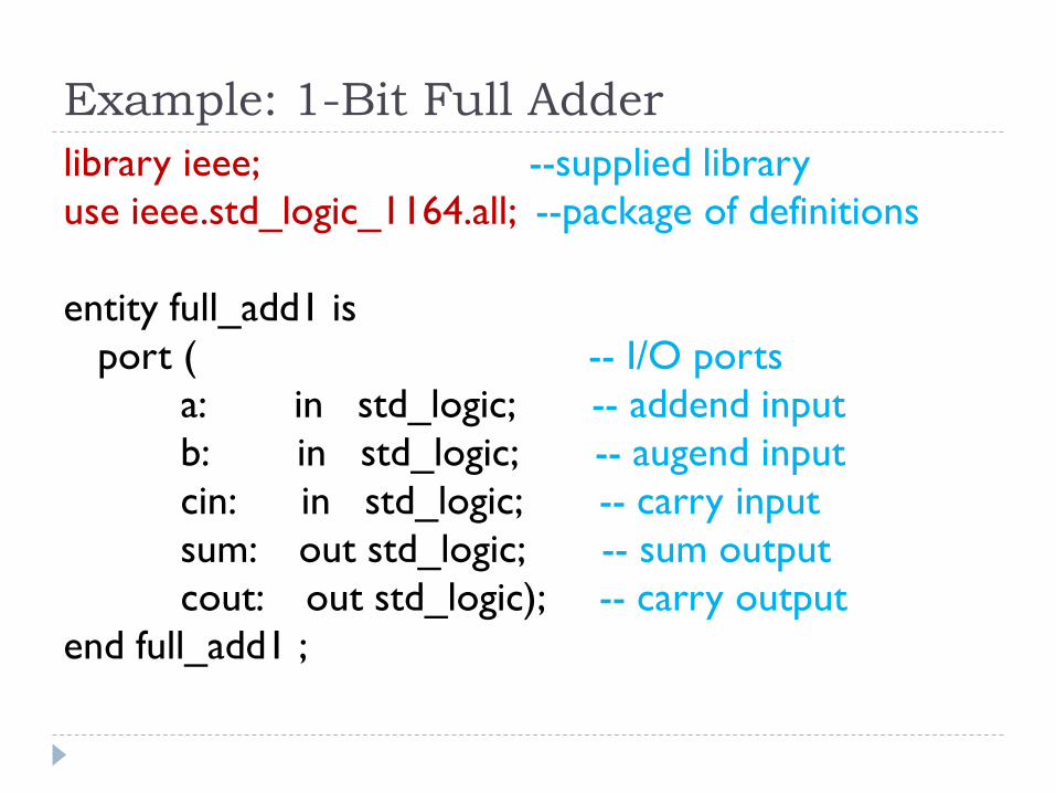
Example: 1-Bit Full Adderlibrary ieee; --supplied libraryuse ieee.std_logic_1164.all; --package of definitions
entity full_add1 isport ( -- I/O ports
a: in std_logic; -- addend inputb: in std_logic; -- augend inputcin: in std_logic; -- carry inputsum: out std_logic; -- sum outputcout: out std_logic); -- carry output
end full_add1 ;
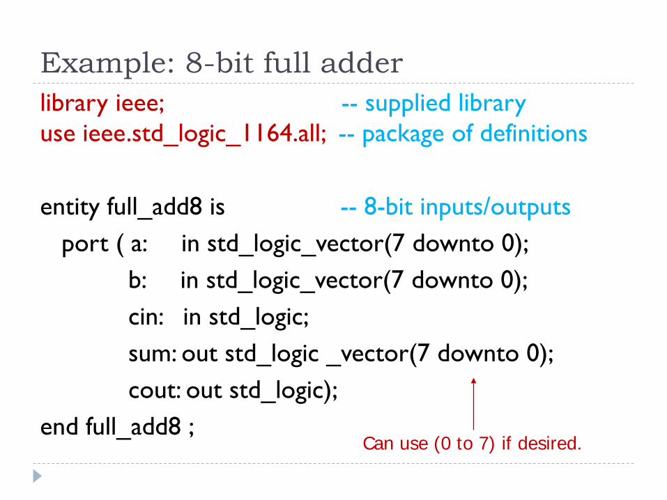
Example: 8-bit full adderlibrary ieee; -- supplied libraryuse ieee.std_logic_1164.all; -- package of definitions
entity full_add8 is -- 8-bit inputs/outputsport ( a: in std_logic_vector(7 downto 0);
b: in std_logic_vector(7 downto 0);cin: in std_logic;sum: out std_logic _vector(7 downto 0);cout: out std_logic);
end full_add8 ;Can use (0 to 7) if desired.
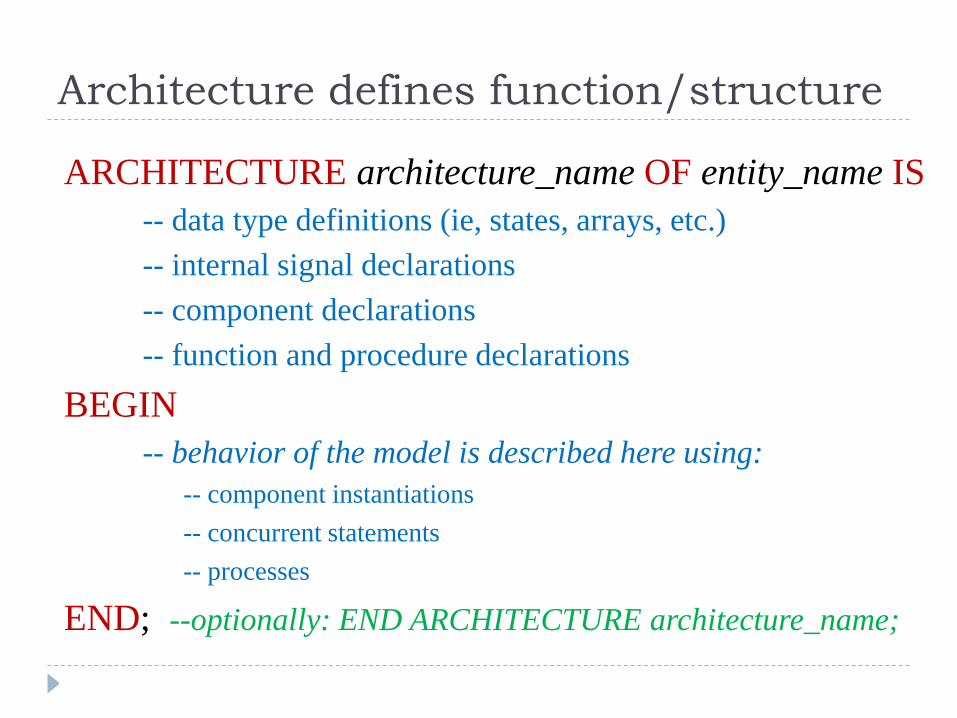
Architecture defines function/structure
ARCHITECTURE architecture_name OF entity_name IS-- data type definitions (ie, states, arrays, etc.)-- internal signal declarations-- component declarations-- function and procedure declarations
BEGIN-- behavior of the model is described here using:
-- component instantiations-- concurrent statements-- processes
END; --optionally: END ARCHITECTURE architecture_name;
ELEC2200-001 Fall 2010, Nov 2
20
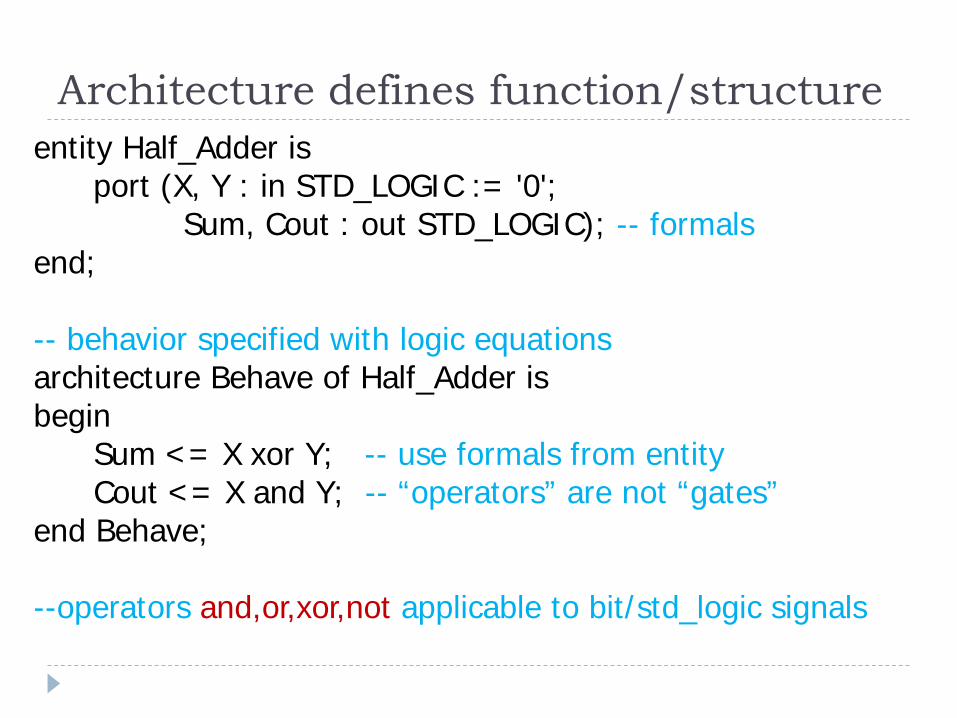
entity Half_Adder isport (X, Y : in STD_LOGIC := '0';
Sum, Cout : out STD_LOGIC); -- formals end;
-- behavior specified with logic equationsarchitecture Behave of Half_Adder isbegin
Sum <= X xor Y; -- use formals from entityCout <= X and Y; -- “operators” are not “gates”
end Behave;
--operators and,or,xor,not applicable to bit/std_logic signals
Architecture defines function/structure
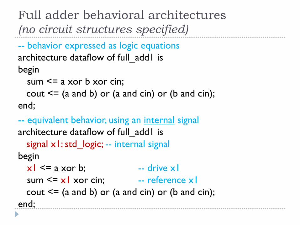
Full adder behavioral architectures (no circuit structures specified)-- behavior expressed as logic equationsarchitecture dataflow of full_add1 isbegin
sum <= a xor b xor cin;cout <= (a and b) or (a and cin) or (b and cin);
end;-- equivalent behavior, using an internal signalarchitecture dataflow of full_add1 is
signal x1: std_logic; -- internal signalbegin
x1 <= a xor b; -- drive x1sum <= x1 xor cin; -- reference x1cout <= (a and b) or (a and cin) or (b and cin);
end;
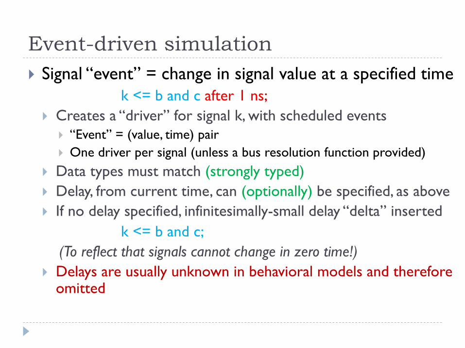
Event-driven simulation Signal “event” = change in signal value at a specified time
k <= b and c after 1 ns; Creates a “driver” for signal k, with scheduled events
“Event” = (value, time) pair One driver per signal (unless a bus resolution function provided)
Data types must match (strongly typed) Delay, from current time, can (optionally) be specified, as above If no delay specified, infinitesimally-small delay “delta” inserted
k <= b and c; (To reflect that signals cannot change in zero time!)
Delays are usually unknown in behavioral models and therefore omitted
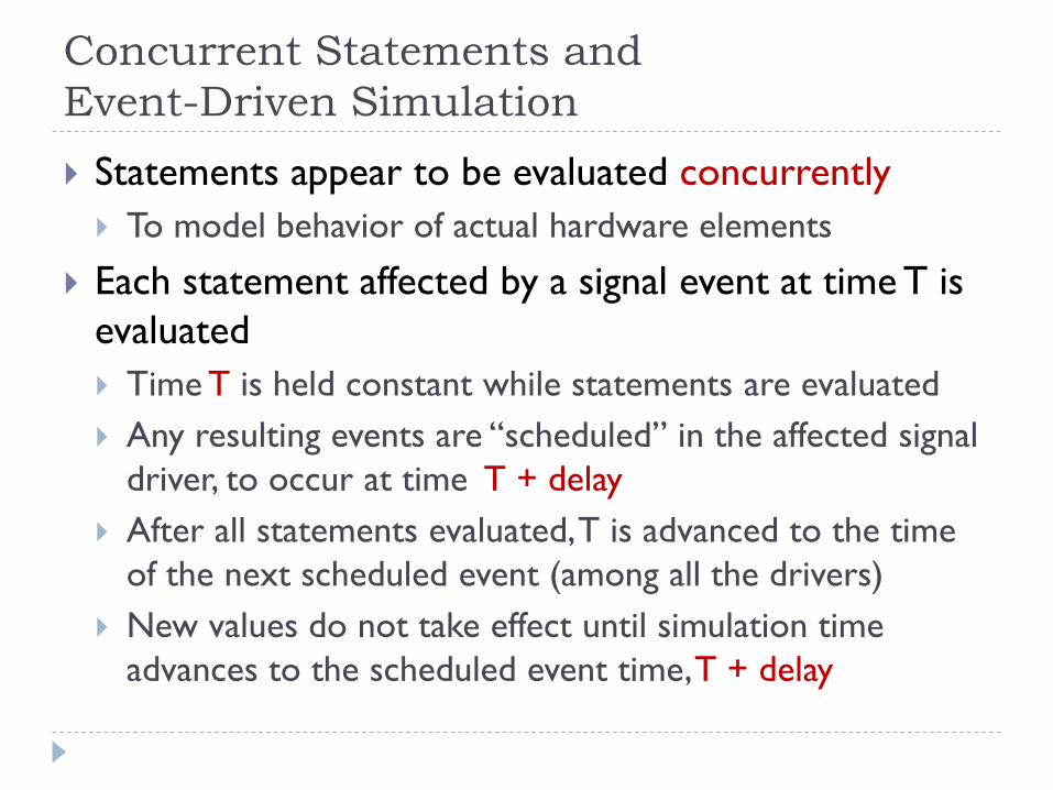
Concurrent Statements and Event-Driven Simulation Statements appear to be evaluated concurrently To model behavior of actual hardware elements
Each statement affected by a signal event at time T is evaluated Time T is held constant while statements are evaluated Any resulting events are “scheduled” in the affected signal
driver, to occur at time T + delay After all statements evaluated, T is advanced to the time
of the next scheduled event (among all the drivers) New values do not take effect until simulation time
advances to the scheduled event time, T + delay
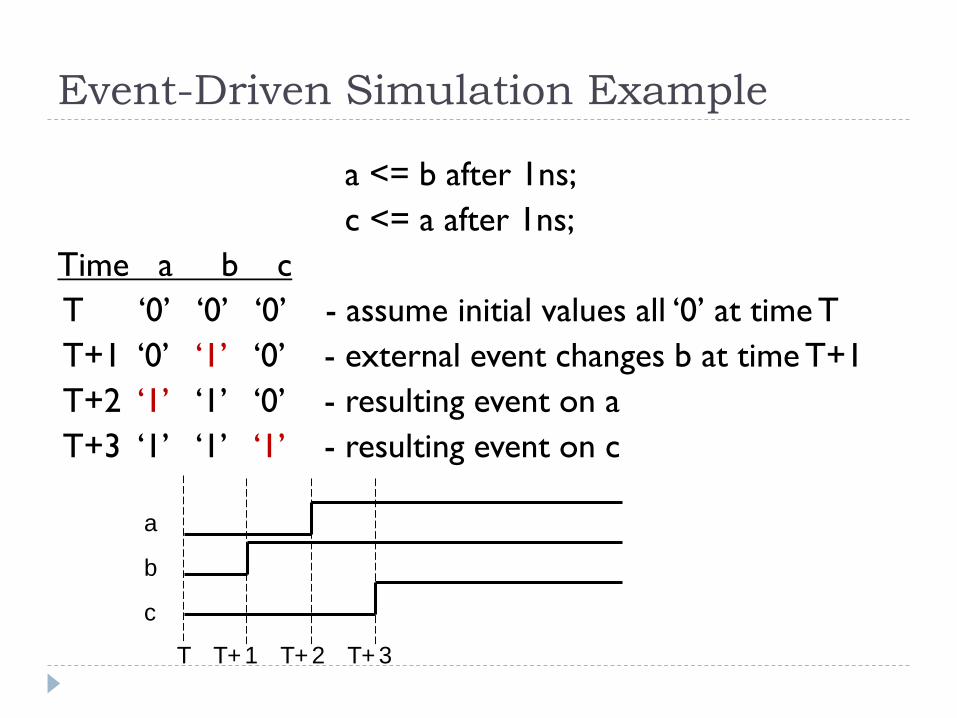
Event-Driven Simulation Example
a <= b after 1ns;c <= a after 1ns;
Time a b cT ‘0’ ‘0’ ‘0’ - assume initial values all ‘0’ at time TT+1 ‘0’ ‘1’ ‘0’ - external event changes b at time T+1T+2 ‘1’ ‘1’ ‘0’ - resulting event on a T+3 ‘1’ ‘1’ ‘1’ - resulting event on c
a
b
c
T T+1 T+2 T+3
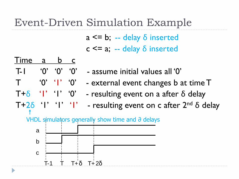
Event-Driven Simulation Examplea <= b; -- delay δ insertedc <= a; -- delay δ inserted
Time a b cT-1 ‘0’ ‘0’ ‘0’ - assume initial values all ‘0’T ‘0’ ‘1’ ‘0’ - external event changes b at time TT+δ ‘1’ ‘1’ ‘0’ - resulting event on a after δ delayT+2δ ‘1’ ‘1’ ‘1’ - resulting event on c after 2nd δ delay
VHDL simulators generally show time and ∂ delays
a
b
c
T-1 T T+δ T+2δ


![VHDL 3 – Sequential Logic Circuitsnelson/courses/elec4200/Slides/VHDL 3... · ... variable k is “implied” in the for-loop and does not ... General format: Example: [label:]](https://static.documents.pub/doc/80x56/5ae82c3b7f8b9a6d4f8f2324/vhdl-3-sequential-logic-nelsoncourseselec4200slidesvhdl-3-variable.jpg)


