Modeling Physical PCB Effects 5& 1 Abstract Getting logical designs to meet specifications is the first step in creating a manufacturable design. Getting the physical design to work is the next step. The physical effects of PCB materials, transmission lines, vias, and trace coupling can all cause a working logical design to fail. However, you can predict these effects before getting to the prototype stage. This module uses Agilent EEsof EDA’s physical design tools to characterize the PCB design in order to minimize prototype turns.
Transcript
Modeling Physical PCB Effects �&
1
AbstractGetting logical designs to meet specifications is the first step in creating a manufacturable design.Getting the physical design to work is the next step. The physical effects of PCB materials,transmission lines, vias, and trace coupling can all cause a working logical design to fail. However,you can predict these effects before getting to the prototype stage. This module uses Agilent EEsofEDA’s physical design tools to characterize the PCB design in order to minimize prototype turns.
Modeling Physical PCB Effects �&
2
Gaining the Wireless Edge 2000Techniques for RF and High-Frequency Wireless Design
Modeling Physical PCB Effects
Modeling Physical PCB Effects �&
3
Page 3
Overview
•Fitting physical verification into the overall design flow
•Maintaining component specifications after placement
•Generating an ADS model of a Motorola duplexer
•2D EM characterization of layout
•3D EM characterization of layout
•Pinpointing the design problem and implementing a fix
•Summary
Modeling Physical PCB Effects �&
4
Page 4
DESIGN
FEEDBACK
DESIGN
FEEDBACK
Data ProcessingData Processing
System LibrarySystem Library
Custom ModelsCustom Models
SupportingInfrastructure
INSTRUMENTATION
INSTRUMENTATION
Logical Design
Physical DesignManufacturingManufacturing
System DesignSystem Design
Circuit DesignCircuit Design
LayoutLayout
ConceptConcept
EM Visualization &Optimization
EM Visualization &Optimization
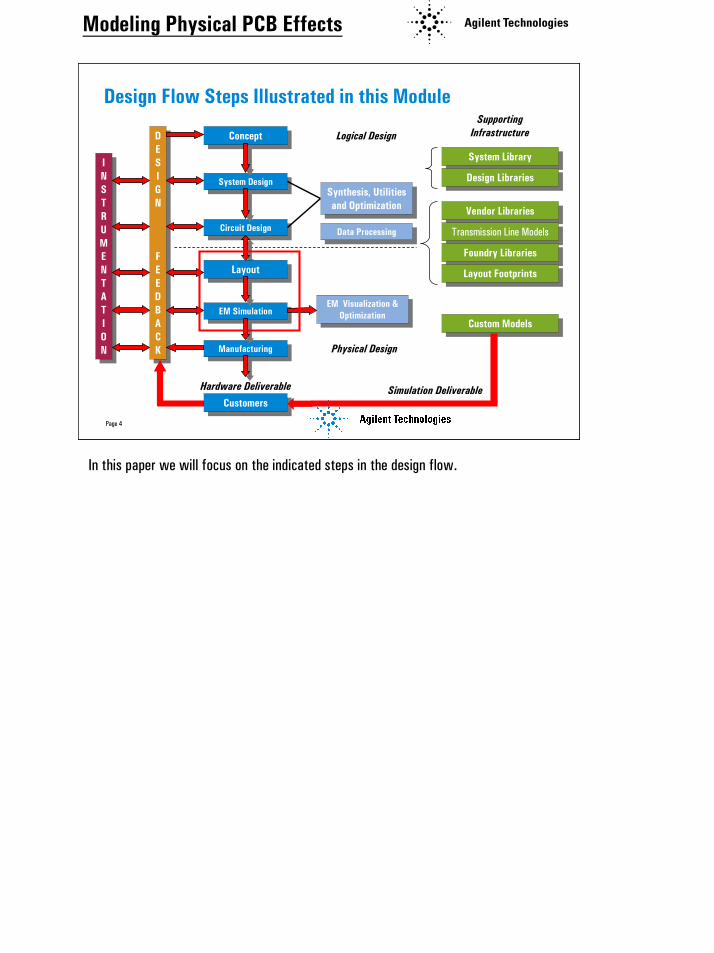
Design Flow Steps Illustrated in this Module
EM SimulationEM Simulation
Design LibrariesDesign Libraries
Simulation DeliverableHardware Deliverable
CustomersCustomers
Synthesis, Utilitiesand Optimization
Synthesis, Utilitiesand Optimization
Vendor LibrariesVendor Libraries
Transmission Line ModelsTransmission Line Models
Foundry LibrariesFoundry Libraries
Layout FootprintsLayout Footprints
In this paper we will focus on the indicated steps in the design flow.
Both Needs Affect The Single-Tone Desensitization Specification!
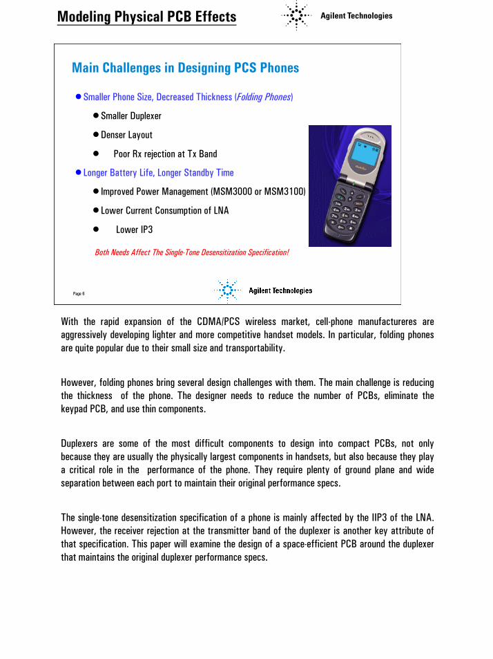
With the rapid expansion of the CDMA/PCS wireless market, cell-phone manufactureres areaggressively developing lighter and more competitive handset models. In particular, folding phonesare quite popular due to their small size and transportability.
However, folding phones bring several design challenges with them. The main challenge is reducingthe thickness of the phone. The designer needs to reduce the number of PCBs, eliminate thekeypad PCB, and use thin components.
Duplexers are some of the most difficult components to design into compact PCBs, not onlybecause they are usually the physically largest components in handsets, but also because they playa critical role in the performance of the phone. They require plenty of ground plane and wideseparation between each port to maintain their original performance specs.
The single-tone desensitization specification of a phone is mainly affected by the IIP3 of the LNA.However, the receiver rejection at the transmitter band of the duplexer is another key attribute ofthat specification. This paper will examine the design of a space-efficient PCB around the duplexerthat maintains the original duplexer performance specs.
Modeling Physical PCB Effects �&
7
Page 7
-30 dBm
-101 dBm1840~1870 MHz
-24(28) dBm1750~1780 MHz
90 MHz 12.5 MHz
Tx Band
Rx Band
Jammer
Single-Tone Desensitization
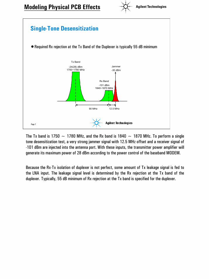
•Required Rx rejection at the Tx Band of the Duplexer is typically 55 dB minimum
The Tx band is 1750 ~ 1780 MHz, and the Rx band is 1840 ~ 1870 MHz. To perform a singletone desensitization test, a very strong jammer signal with 12.5 MHz offset and a receiver signal of-101 dBm are injected into the antenna port. With these inputs, the transmitter power amplifier willgenerate its maximum power of 28 dBm according to the power control of the baseband MODEM.
Because the Rx-Tx isolation of duplexer is not perfect, some amount of Tx leakage signal is fed tothe LNA input. The leakage signal level is determined by the Rx rejection at the Tx band of theduplexer. Typically, 55 dB minimum of Rx rejection at the Tx band is specified for the duplexer.
Modeling Physical PCB Effects �&
8
Page 8
Example: A real board
currently in massproduction
Antenna Connector
DuplexerIsolator LNA
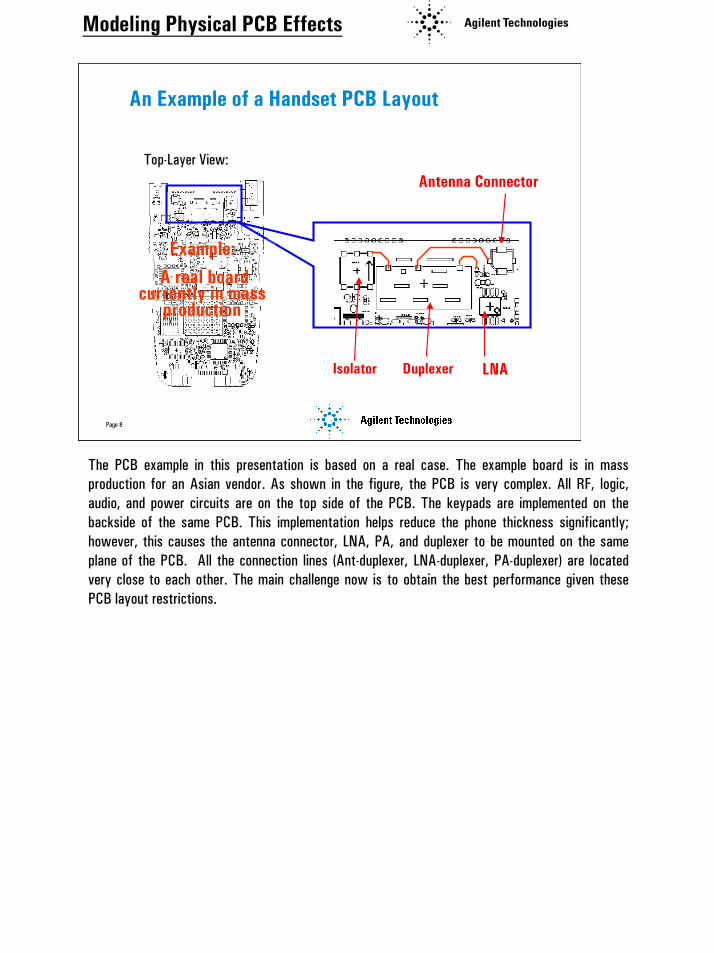
An Example of a Handset PCB Layout
Top-Layer View:
The PCB example in this presentation is based on a real case. The example board is in massproduction for an Asian vendor. As shown in the figure, the PCB is very complex. All RF, logic,audio, and power circuits are on the top side of the PCB. The keypads are implemented on thebackside of the same PCB. This implementation helps reduce the phone thickness significantly;however, this causes the antenna connector, LNA, PA, and duplexer to be mounted on the sameplane of the PCB. All the connection lines (Ant-duplexer, LNA-duplexer, PA-duplexer) are locatedvery close to each other. The main challenge now is to obtain the best performance given thesePCB layout restrictions.
Modeling Physical PCB Effects �&
9
Page 9
Frequency Typical Spec(MHz) (@25oC)
Ant to Tx ResponsePass Band Insertion Loss 1750-1780 1.7 dBPass Band Return Loss 1750-1780 15.0 dB
Rejection @ Rx Band 1840-1870 45.0 dBAnt to Rx Response
Pass Band Insertion Loss 1840-1870 2.5 dBPass Band Return Loss 1840-1870 15.0 dB
Rejection @ Tx Band 1750-1780 60.0 dBTx to Rx Response
Rejection @ Tx Band 1750-1780 61.0 dBRejection @ Rx Band 1840-1870 46.0 dB
Parameter
Monoblock Duplexer
KFF6614, 3mm height, Motorola: Specifications from datasheet
Focus on this Specification:Rejection at Tx Band 1750-1780 MHzis 60 dB
The duplexer used in this design is a monoblock type. It's only 3 mm thick, yet it is still the thickestcomponent. The specifications in the datasheet are good, but this is de-embedded data and does notinclude the performance degradation when mounted on a general PCB.
Modeling Physical PCB Effects �&
10
Page 10
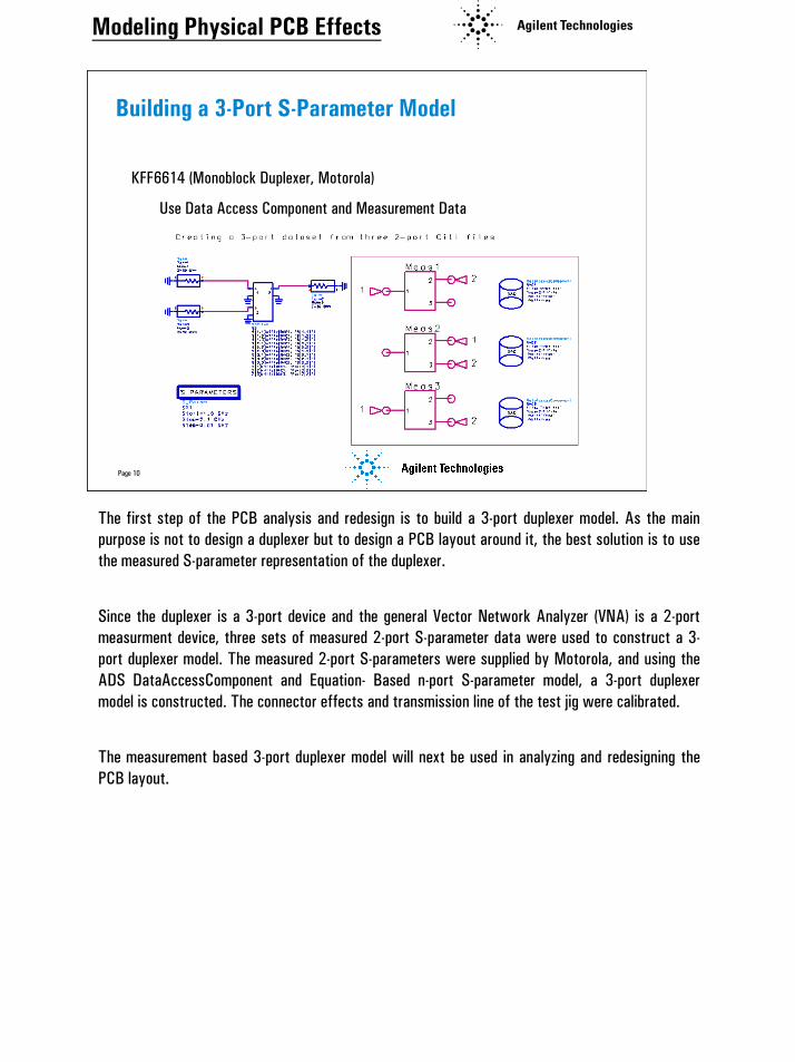
Building a 3-Port S-Parameter Model
KFF6614 (Monoblock Duplexer, Motorola)
Use Data Access Component and Measurement Data
The first step of the PCB analysis and redesign is to build a 3-port duplexer model. As the mainpurpose is not to design a duplexer but to design a PCB layout around it, the best solution is to usethe measured S-parameter representation of the duplexer.
Since the duplexer is a 3-port device and the general Vector Network Analyzer (VNA) is a 2-portmeasurment device, three sets of measured 2-port S-parameter data were used to construct a 3-port duplexer model. The measured 2-port S-parameters were supplied by Motorola, and using theADS DataAccessComponent and Equation- Based n-port S-parameter model, a 3-port duplexermodel is constructed. The connector effects and transmission line of the test jig were calibrated.
The measurement based 3-port duplexer model will next be used in analyzing and redesigning thePCB layout.
Modeling Physical PCB Effects �&
11
Page 11
Tx Band Rx Band Original Rx rejection @ Tx Band >60 dB
Ultimate rejectionis 62 dB and theinsertion loss is3 dB
→ The totalisolation required onthe PCB is 65 dB min
Insertion Loss: Antenna to Rx, Antenna to Tx
Measurement-Based 3-Port Duplexer Model
The graph above shows the transmission characteristics of the duplexer model. Because themounting effects are not included, the Rx rejection at the Tx band is very good (below -62 dB). Tomaintain this performance after mounting, the port isolation of the board should be greater than65dB. The suppression of PCB feedthrough is the main focus. The required board isolation of 65 dBis possible with a careful design of the PCB layout.
Modeling Physical PCB Effects �&
12
Page 12
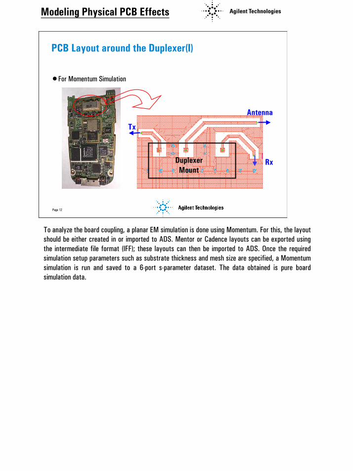
PCB Layout around the Duplexer(I)
•For Momentum Simulation
RxDuplexerMount
Tx
Antenna
To analyze the board coupling, a planar EM simulation is done using Momentum. For this, the layoutshould be either created in or imported to ADS. Mentor or Cadence layouts can be exported usingthe intermediate file format (IFF); these layouts can then be imported to ADS. Once the requiredsimulation setup parameters such as substrate thickness and mesh size are specified, a Momentumsimulation is run and saved to a 6-port s-parameter dataset. The data obtained is pure boardsimulation data.
Modeling Physical PCB Effects �&
13
Page 13
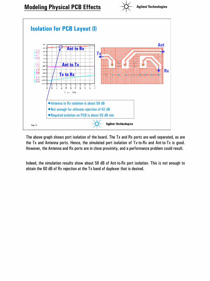
Isolation for PCB Layout (I)
AntAnt to Rx
Ant to Tx
Tx to Rx
Tx
Rx
•Antenna to Rx isolation is about 58 dB•Not enough for ultimate rejection of 62 dB•Required isolation on PCB is about 65 dB min
The above graph shows port isolation of the board. The Tx and Rx ports are well separated, as arethe Tx and Antenna ports. Hence, the simulated port isolation of Tx-to-Rx and Ant-to-Tx is good.However, the Antenna and Rx ports are in close proximity, and a performance problem could result.
Indeed, the simulation results show about 58 dB of Ant-to-Rx port isolation. This is not enough toobtain the 60 dB of Rx rejection at the Tx band of duplexer that is desired.
Modeling Physical PCB Effects �&
14
Page 14
Simulation Results for Layout (I)
•Duplexer Model & Momentum
15.6 dB
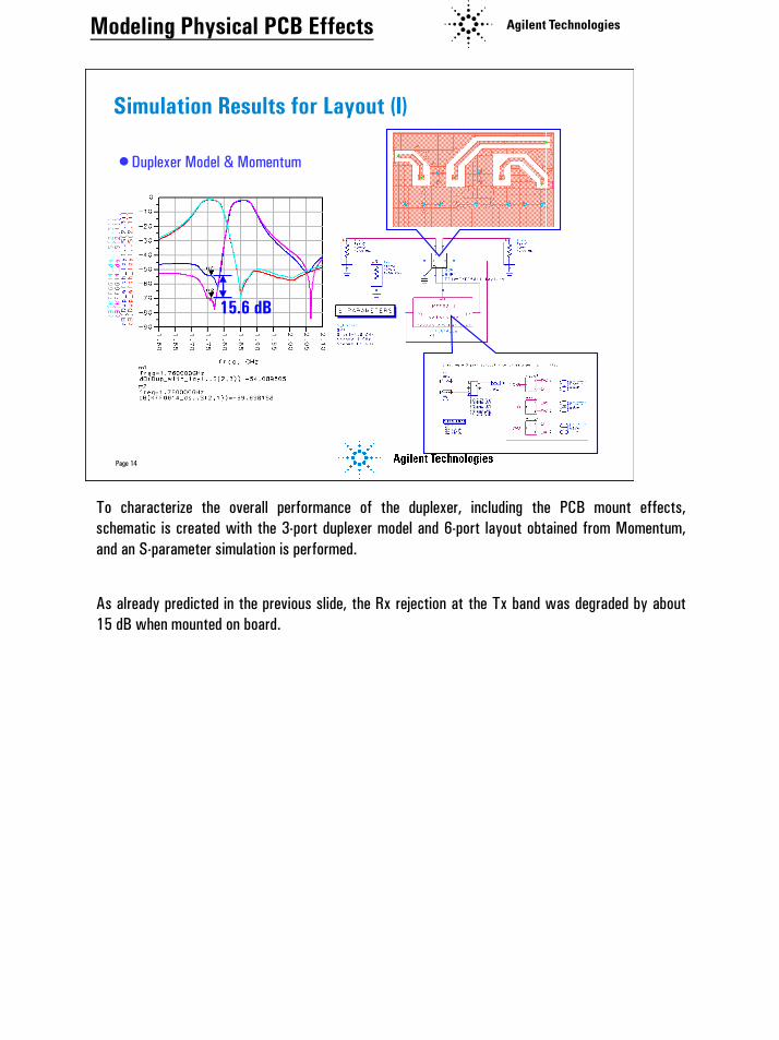
To characterize the overall performance of the duplexer, including the PCB mount effects,schematic is created with the 3-port duplexer model and 6-port layout obtained from Momentum,and an S-parameter simulation is performed.
As already predicted in the previous slide, the Rx rejection at the Tx band was degraded by about15 dB when mounted on board.
Modeling Physical PCB Effects �&
15
Page 15
PCB Layout around the Duplexer (II)Via Holes for Preventing FieldCoupling through the Substrate
DuplexerMount
Antenna Line
Rx Line
The main reason for port isolation degradation is feedthrough. That is, some amount of field at theAntenna line is coupled to the field of the Rx line at some location in the board. But at this moment,it is not known where this coupling is located. Most likely, there is coupling through the inside ofthe substrate. To prevent this, via holes are added between the Antenna line and Rx line. These viaholes should prevent some degree of field leakage.
Modeling Physical PCB Effects �&
16
Page 16
Isolation for PCB Layout (II)
Ant
Ant to Rx
Ant to Tx
Tx to RxRx
Tx
•Antenna to Rx isolation is still 58 dB
•Not enough for ultimate rejection of 62 dB
•Required isolation on PCB is ~65 dB min
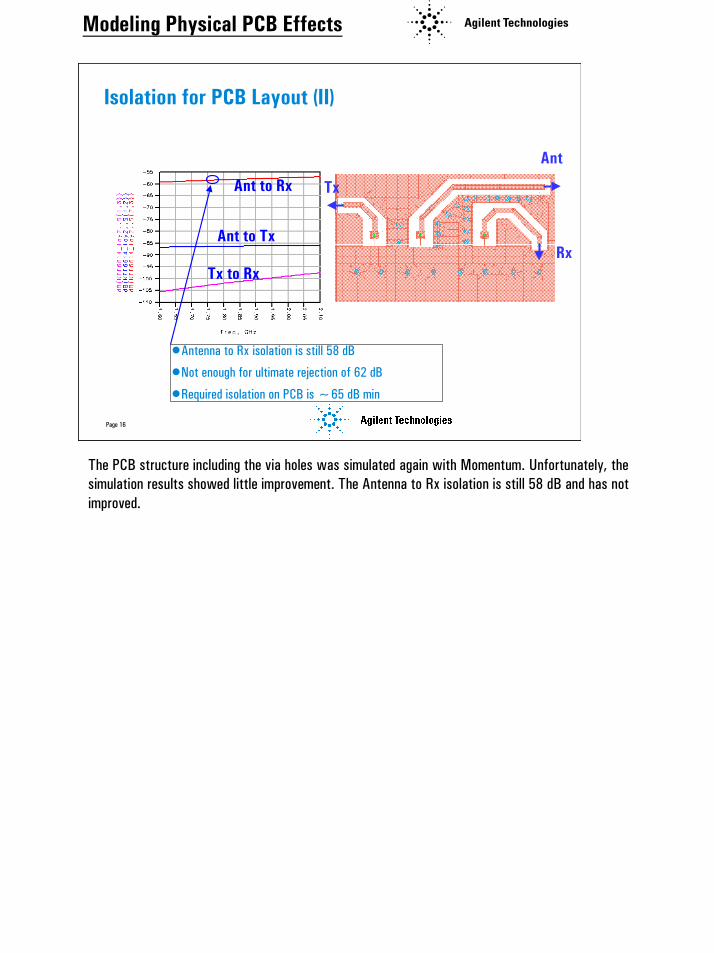
The PCB structure including the via holes was simulated again with Momentum. Unfortunately, thesimulation results showed little improvement. The Antenna to Rx isolation is still 58 dB and has notimproved.
Modeling Physical PCB Effects �&
17
Page 17
15.3 dB
Simulation Results For Layout (II)
•Duplexer Model & Momentum
Again, the overall characteristics of the duplexer are simulated, including the PCB and via holeeffects. The Rx rejection at the Tx band of the duplexer improved slightly, but the value isnegligible.
For confirmation of these results, the design is exported to Agilent HFSS for further analysis.Agilent HFSS is a full 3-D EM simulator based on the finite element method.
Modeling Physical PCB Effects �&
18
Page 18
Extra microstrip lines are de-embedded in the post-processor
3D EM-Simulation: Agilent HFSS
•ADS/Momentum Layout Translation to HFSS
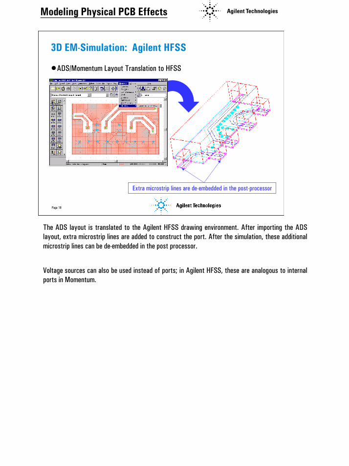
The ADS layout is translated to the Agilent HFSS drawing environment. After importing the ADSlayout, extra microstrip lines are added to construct the port. After the simulation, these additionalmicrostrip lines can be de-embedded in the post processor.
Voltage sources can also be used instead of ports; in Agilent HFSS, these are analogous to internalports in Momentum.
Modeling Physical PCB Effects �&
19
Page 19
Isolation for PCB Layout (II) -- 3D EM Modeling
Tx
Ant to Rx
Ant to Tx
Tx to Rx
Ant
•Ant to Rx isolation is still 60 dB
•Still not enough for an ultimate rejection of 62 dB
•Required isolation on PCB is ~65 dB min
Rx
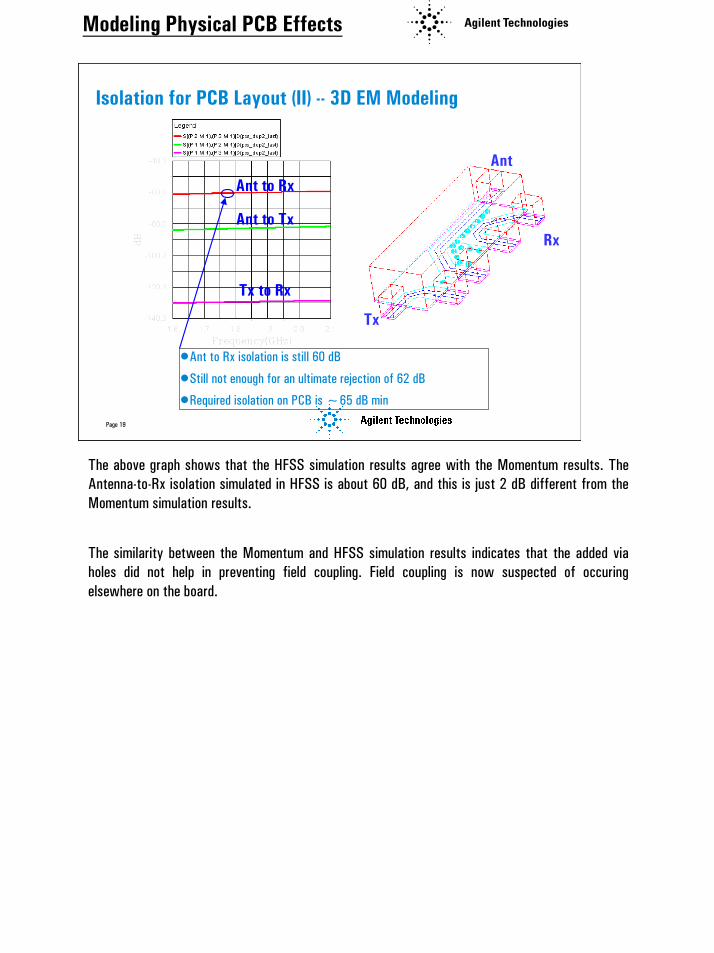
The above graph shows that the HFSS simulation results agree with the Momentum results. TheAntenna-to-Rx isolation simulated in HFSS is about 60 dB, and this is just 2 dB different from theMomentum simulation results.
The similarity between the Momentum and HFSS simulation results indicates that the added viaholes did not help in preventing field coupling. Field coupling is now suspected of occuringelsewhere on the board.
Modeling Physical PCB Effects �&
20
Page 20
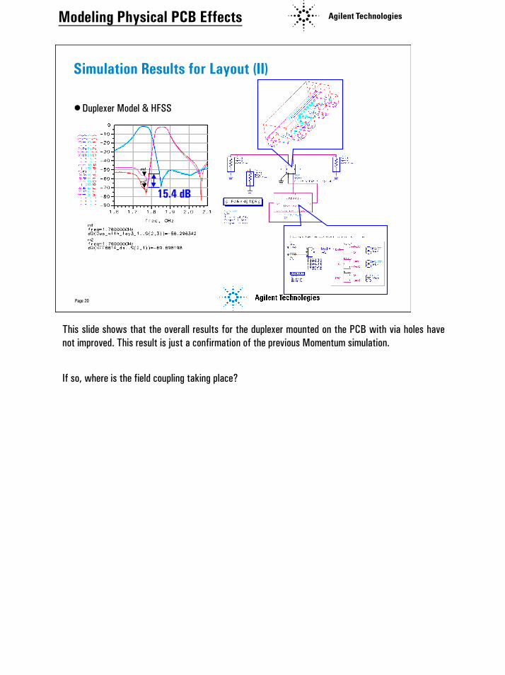
15.4 dB
Simulation Results for Layout (II)
•Duplexer Model & HFSS
This slide shows that the overall results for the duplexer mounted on the PCB with via holes havenot improved. This result is just a confirmation of the previous Momentum simulation.
If so, where is the field coupling taking place?
Modeling Physical PCB Effects �&
21
Page 21
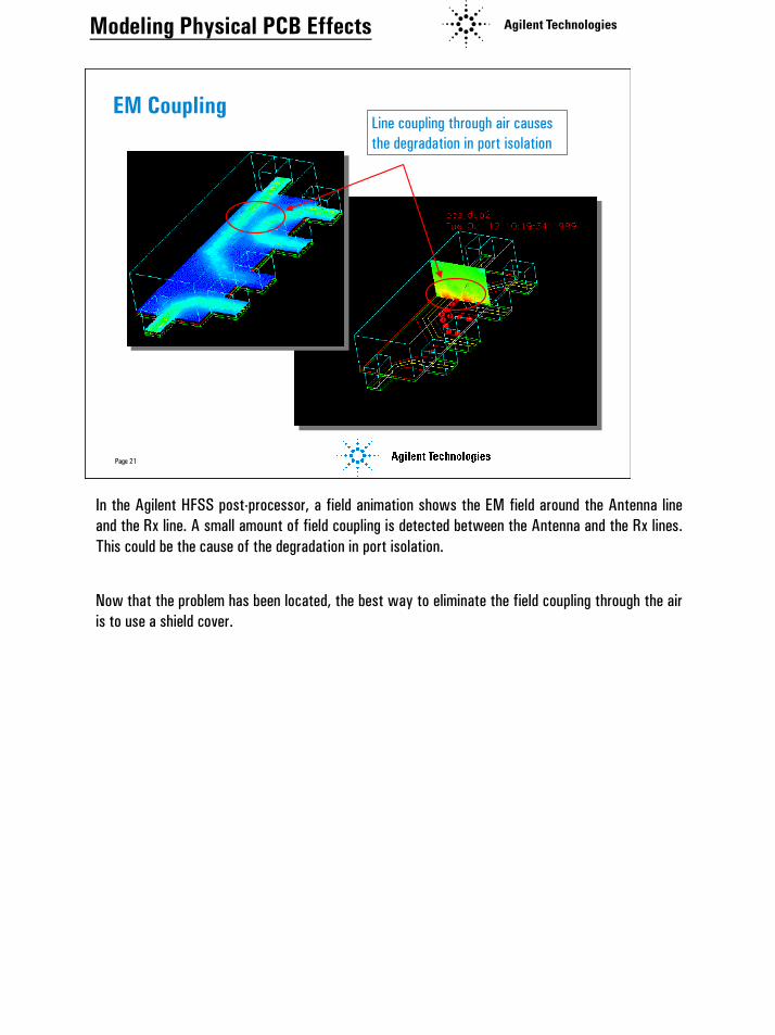
EM CouplingLine coupling through air causesthe degradation in port isolation
In the Agilent HFSS post-processor, a field animation shows the EM field around the Antenna lineand the Rx line. A small amount of field coupling is detected between the Antenna and the Rx lines.This could be the cause of the degradation in port isolation.
Now that the problem has been located, the best way to eliminate the field coupling through the airis to use a shield cover.
Modeling Physical PCB Effects �&
22
Page 22
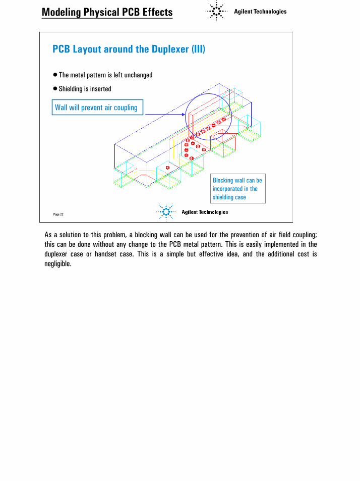
Blocking wall can beincorporated in theshielding case
PCB Layout around the Duplexer (III)
•The metal pattern is left unchanged
•Shielding is inserted
Wall will prevent air coupling
As a solution to this problem, a blocking wall can be used for the prevention of air field coupling;this can be done without any change to the PCB metal pattern. This is easily implemented in theduplexer case or handset case. This is a simple but effective idea, and the additional cost isnegligible.
Modeling Physical PCB Effects �&
23
Page 23
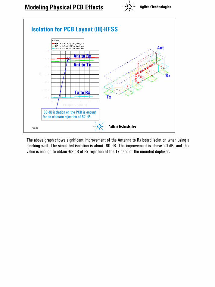
Isolation for PCB Layout (III)-HFSS
Rx
Ant
Tx
80 dB isolation on the PCB is enoughfor an ultimate rejection of 62 dB
Ant to Rx
Ant to Tx
Tx to Rx
The above graph shows significant improvement of the Antenna to Rx board isolation when using ablocking wall. The simulated isolation is about -80 dB. The improvement is above 20 dB, and thisvalue is enough to obtain -62 dB of Rx rejection at the Tx band of the mounted duplexer.
Modeling Physical PCB Effects �&
24
Page 24
Very close to theoriginal duplexer specs
Simulation Results for Layout (III)
•Duplexer Model & HFSS
A schematic with the 3-port duplexer model and the S-parameter data from Agilent HFSS iscreated. The simulation results for this modified design are nearly identical to the originalunmounted duplexer specifications. Both results show more than 60 dB of Rx rejection at the Txband.
Modeling Physical PCB Effects �&
25
Page 25
Measurement Results
~18dB
Without Blocking Wall
With Blocking Wall
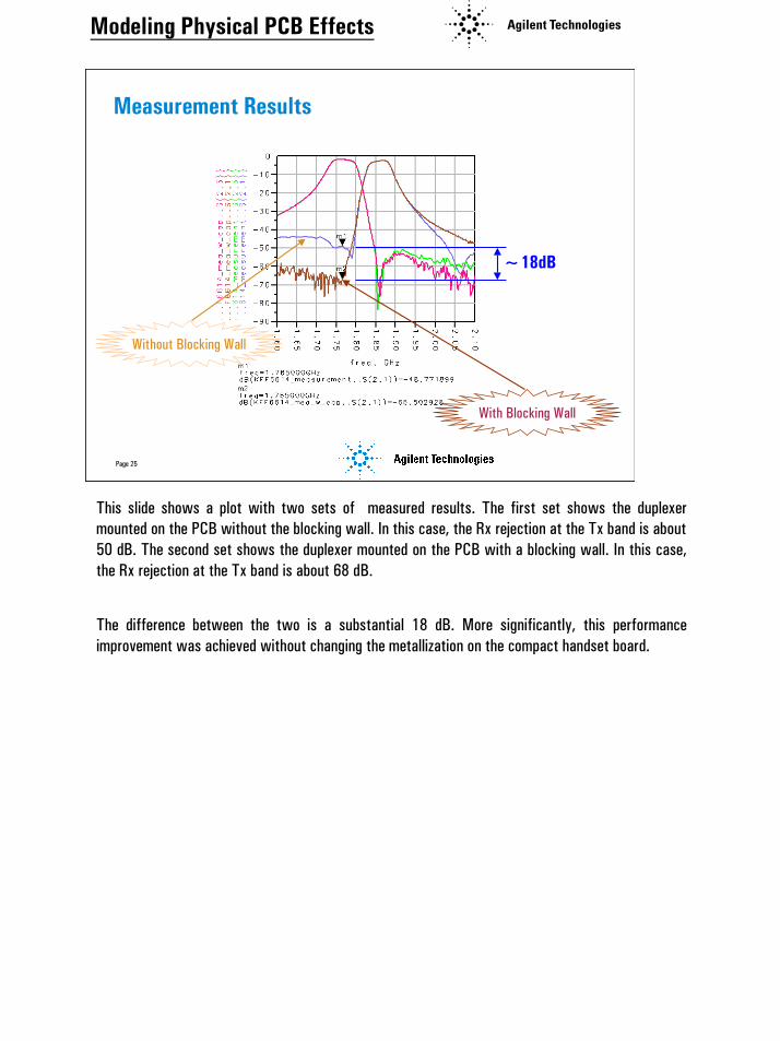
This slide shows a plot with two sets of measured results. The first set shows the duplexermounted on the PCB without the blocking wall. In this case, the Rx rejection at the Tx band is about50 dB. The second set shows the duplexer mounted on the PCB with a blocking wall. In this case,the Rx rejection at the Tx band is about 68 dB.
The difference between the two is a substantial 18 dB. More significantly, this performanceimprovement was achieved without changing the metallization on the compact handset board.
Modeling Physical PCB Effects �&
26
Page 26
Summary
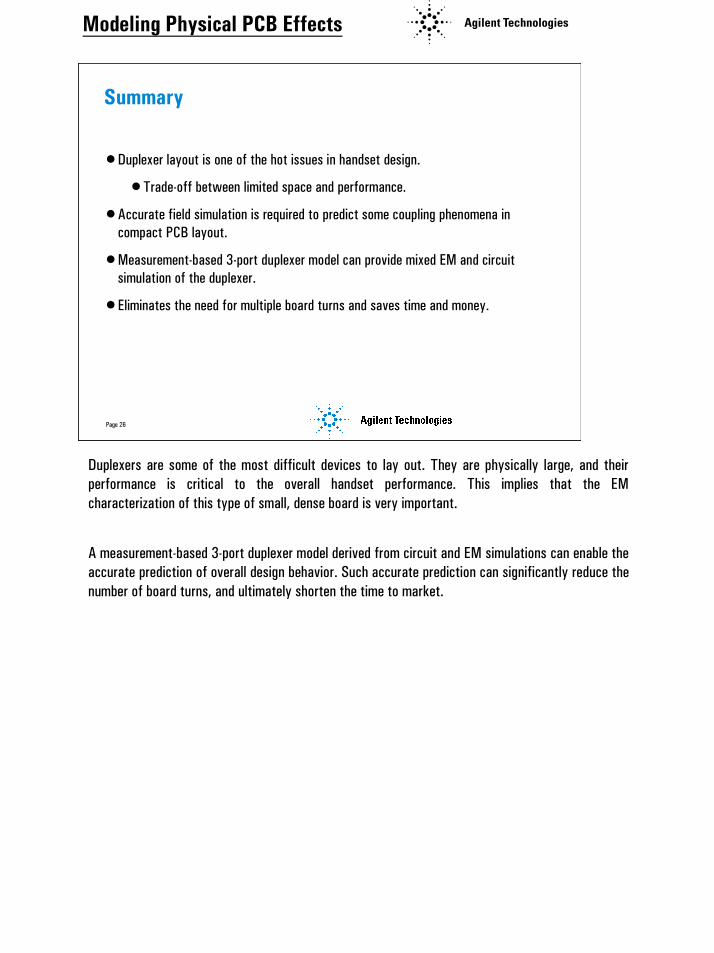
•Duplexer layout is one of the hot issues in handset design.
•Trade-off between limited space and performance.
•Accurate field simulation is required to predict some coupling phenomena incompact PCB layout.
•Measurement-based 3-port duplexer model can provide mixed EM and circuitsimulation of the duplexer.
•Eliminates the need for multiple board turns and saves time and money.
Duplexers are some of the most difficult devices to lay out. They are physically large, and theirperformance is critical to the overall handset performance. This implies that the EMcharacterization of this type of small, dense board is very important.
A measurement-based 3-port duplexer model derived from circuit and EM simulations can enable theaccurate prediction of overall design behavior. Such accurate prediction can significantly reduce thenumber of board turns, and ultimately shorten the time to market.