Page 1
i
The Pennsylvania State University
The Graduate School
Materials Science and Engineering
MODIFICATION OF METAL INSULATOR TRANSITION IN ULTRATHIN VO2
FILMS VIA ULTRA VIOLET RADIATION
A Thesis in
Materials Science and Engineering
by
Lu Guo
Submitted in Partial Fulfillment
of the Requirement
for the Degree of
Master of Science
December 2014
Page 2
ii
The thesis of Lu Guo was reviewed and approved* by the following:
Venkatraman Gopalan
Professor of Materials Science and Engineering
Thesis Advisor
Roman Engel-Herbert
Assistant Professor of Materials Science and Engineering
John V. Badding
Professor of Chemistry
Suzanne Mohney
Professor of Materials Science and Engineering and Electrical Engineering Chair,
Intercollege Graduate Degree Program in Materials Science and Engineering
*Signatures are on file in the Graduate School
Page 3
iii
Abstract
VO2 exhibits metal-insulating transition as a function of temperature, which
makes it one of the prototypical strongly correlated materials. External factors such as
pressure, strain and electrical field can trigger this first order phase transition. The
dramatic property changes as well as the fast transition time make VO2 a promising
candidate for switching devices. In our study, we point out a new way to not only take
advantage of the MIT in VO2 but also to manipulate it. We demonstrate light-induced
modification of the metal-insulator transition in single crystalline VO2 ultrathin films (10
nm) grown on (001) TiO2 substrates. Exposure to 365 nm UV light at 0.19 W/cm2 in non-
oxidizing atmosphere caused the films to remain metallic even when temperatures were
below transition temperature. Post-annealing in oxidizing atmosphere successfully
recovered the MIT transition. Oxygen vacancies formation is proposed to be the
mechanism for this MIT suppression. The ability to eliminate and recover the MIT of
VO2 film presents a flexible way to build electronic circuits using correlated oxides.
Page 4
iv
Table of Contents
List of Figures ................................................................................................................................. v
List of Tables ................................................................................................................................. ix
Acknowledgements ....................................................................................................................... xi
Chapter 1 Background .................................................................................................................. 1
Chapter 2 Electrical Characterization of Transport Properties ............................................... 9
2.1 Two Terminal Devices Fabrication .................................................................................... 9
2.2 Measurement of the UV Irradiated VO2 Films ............................................................... 10
2.3 Measurement of VO2 Films under Different Post-annealing Atmosphere ................... 13
2.4 Hall Measurement of VO2 Thin Films ............................................................................. 16
2.5 Secondary Ion Mass Spectrometry of VO2 Thin Films .................................................. 20
2.6 Summary ............................................................................................................................. 24
Chapter 3 Optical Characterization on Band Structure via Spectroscopic Ellipsometry .... 25
3.1 Introduction of the Ellipsometry ...................................................................................... 25
3.2 Principle of the Ellipsometry Characterization .............................................................. 27
3.3 Optical Properties of VO2 Thin Film ............................................................................... 30
3.4 Experimental Set-up of Ellipsometry Characterization ................................................ 34
3.5 Measurement of UV Irradiated VO2 Films and Post-annealed VO2 Films under
Different Atmosphere .............................................................................................................. 35
3.6 Summary ............................................................................................................................. 40
Chapter 4 Raman Characterization of Films ............................................................................ 41
4.1 Introduction ........................................................................................................................ 41
4.2 UV Raman Experiments, Results and Discussion ........................................................... 44
4.3 Summary ............................................................................................................................. 48
Chapter 5 Future work ................................................................................................................ 49
Reference ...................................................................................................................................... 50
Appendix ....................................................................................................................................... 53
A. Introduction to RC2 Instrument ........................................................................................ 53
B. Details of oscillators used in Chapter 3 ............................................................................. 54
Page 5
v
List of Figures
Figure 1- 1. Crystal structure of VO2. a) The rutile crystal structure of VO2. b) The M1
phase structure for monoclinic VO2 below transition temperature. c) The M2 phase
structure for monoclinic VO2 below transition temperature. The red balls represent V
atoms and the blue balls represent O
atoms……………………………………………………………………............................2
Figure 1- 2. The structure evolution of VO2 across MIT, from M1 structure to rutile
structure. The blue frame represents the rutile structure of VO2 above transition
temperature. The red frame represents the monoclinic structure of VO2 below transition
temperature. ........................................................................................................................ 3
Figure 1- 3. Resistivity vs. temperature for the 10 nm VO2/TiO2 (001) film. The
transition temperature for heating cycle is around 290 K while that for cooling cycle is
around 275 K....................................................................................................................... 5
Figure 2- 1. A schematic diagram of set-up for transport properties characterization. 365
nm UV light was used for irradiation. The inner contact was connected to voltage source
and the outside electrode was connected to the ground. ................................................... 11
Figure 2- 2. Hysteresis loop measurement after UV irradiation in different atmosphere.
UV irradiation was performed on samples in N2 and O2, respectively. The hysteresis
behavior for those two samples and the pristine one were compared. Arrows marked in
the figure indicated the direction for temperature varying. .............................................. 12
Figure 2- 3. Hysteresis loop for post-annealing in different atmosphere after irradiation
in N2. The hysteresis behavior of Sample A, Sample B and the pristine one were
compared. Arrows marked in the figure indicated the direction for temperature varying.
........................................................................................................................................... 15
Page 6
vi
Figure 2- 4. Hysteresis loop of the samples post-annealed in N2 and O2 atmosphere for
irradiated sample in O2...................................................................................................... 16
Figure 2- 5. The Hall voltage in the metallic (lower line of blue data markers) and
insulating (upper line of red data markers) phases for the VO2 thin film irradiated by UV
light in N2. ......................................................................................................................... 17
Figure 2- 6. Carrier concentration of the VO2 thin film as a function of temperature
before and after UV irradiation in N2 atmosphere. ........................................................... 18
Figure 2- 7. A schematic diagram of work principle of Secondary Ion Mass Spectrometry
(SIMS).[3] .......................................................................................................................... 21
Figure 2- 8. Depth profile of 18O element in Sample E, Sample F and pristine. The
surface of VO2 thin film and the interface between VO2 thin film and TiO2 substrate are
marked. The VO2 thin film region and TiO2 substrate region are marked by yellow and
light grey respectively. The distributions of 18O in the pristine sample, in Sample E and
Sample F are compared. .................................................................................................... 22
Figure 3- 1. The structure for optical models used to obtain the refractive index
information. Such model is based of layered air/film/substrate structure. ....................... 26
Figure 3- 2. A schematic case of an incident light interacting on the surface of the sample.
The superscripts i, r, t represent incident beam, reflection beam and transmitted beam,
respectively. And the subscripts s, p describe s- and p-polarized wave, respectively. ..... 29
Figure 3- 3. The dielectric constant as a function of photon energy for the epitaxial 10nm
VO2/TiO2 (001) at T < Tc (268 K) and at T > Tc (300 K). Dash line displays the
oscillators used in analyzing raw data to obtain dielectric constant. ................................ 32
Figure 3- 4. The schematic diagram for the band structure of VO2.[1] Regions with
different colors represent different bands, marked at the side. The color arrows describe
certain optical transition between bands. EF shows the position where Fermi Level lies. 33
Page 7
vii
Figure 3- 5 a. The schematic diagram of the set up for insitu monitoring how UV
irradiation modified the MIT of VO2 via Spectroscopic Ellipsometry. b. The photo of
Instec heating stage. c. The design diagram of the cover of the Instec (Unit: inch). Grey
area represents the angel holes in the cover. ..................................................................... 34
Figure 3- 6. The extinction coefficient of 10 nm VO2/TiO2 (001) thin film irradiated by
365 nm as a function of exposure time. Different lines represent the extinction coefficient
after different exposure time. ............................................................................................ 35
Figure 3- 7. The comparison among the extinction coefficients for Sample G, Sample H
and the as-grown one respectively. ................................................................................... 37
Figure 3- 8. The comparison among the extinction coefficients for Sample I, Sample J
and the as-grown one. ....................................................................................................... 38
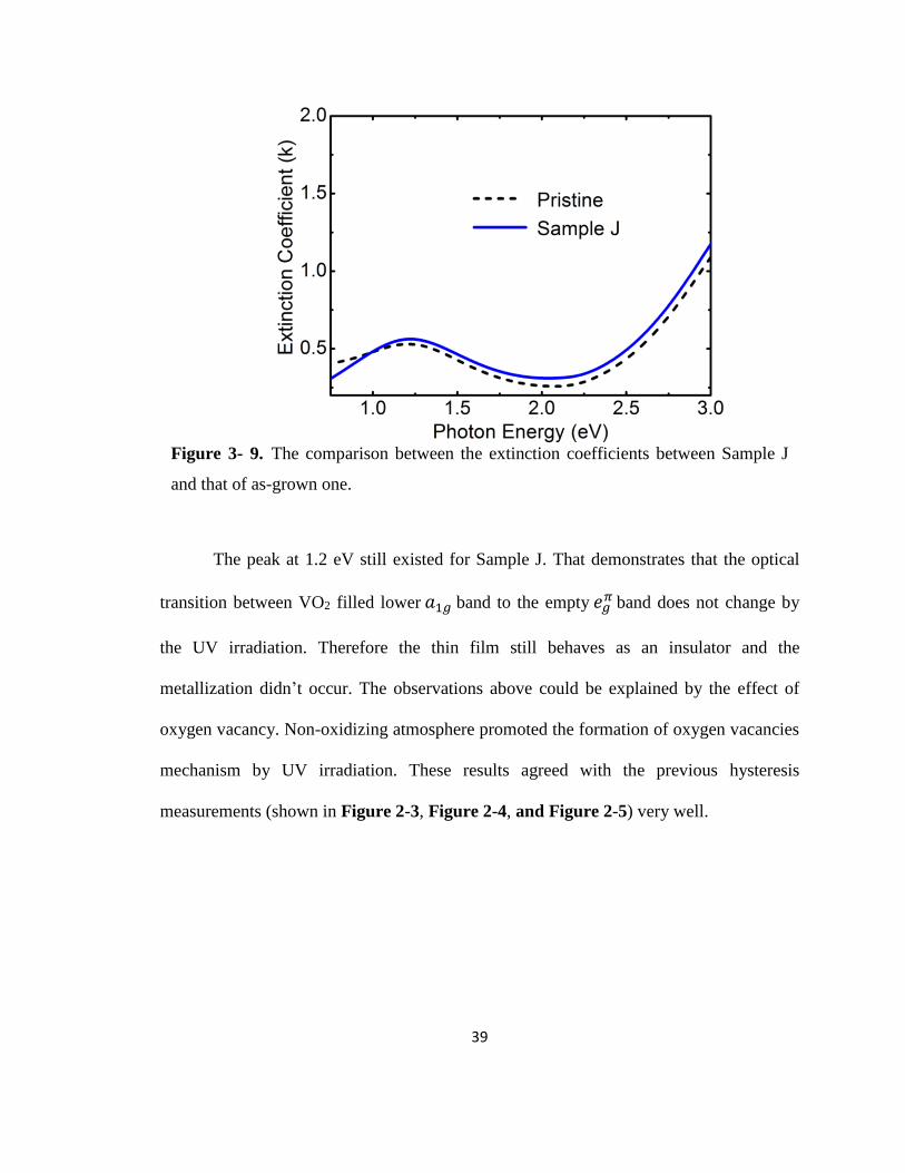
Figure 3- 9. The comparison between the extinction coefficients between Sample J and
that of as-grown one.......................................................................................................... 39
Figure 4- 1. A schematic diagram corresponding to the different types of scattering.[2] . 42
Figure 4- 2. Temperature-dependent Raman Spectrum for VO2/TiO2 (001) thin film. The
temperature increased from 253 K to 293 K, with the internal step of 10 K. Excitation
laser wavelength was 514 nm. .......................................................................................... 44
Figure 4- 3. Temperature-dependent UV Raman Spectrum for 10 nm VO2/TiO2 (001)
thin film. Temperature varies from 253 K to 297 K. Excitation laser wavelength is 257
nm. Dry N2 is purged during cooling process. .................................................................. 46
Page 8
viii
Figure 4- 4. Temperature dependent UV Raman Spectrum for 10nm VO2/TiO
2 (001) thin
film. Temperature varied from 223 K to 298 K. Excitation laser wavelength was 257 nm.
O2 was purged during cooling process.............................................................................. 47
Figure A- 1. The set-up of the multichannel dual-rotating compensator spectroscopic
ellipsometer ....................................................................................................................... 53
Page 9
ix
List of Tables
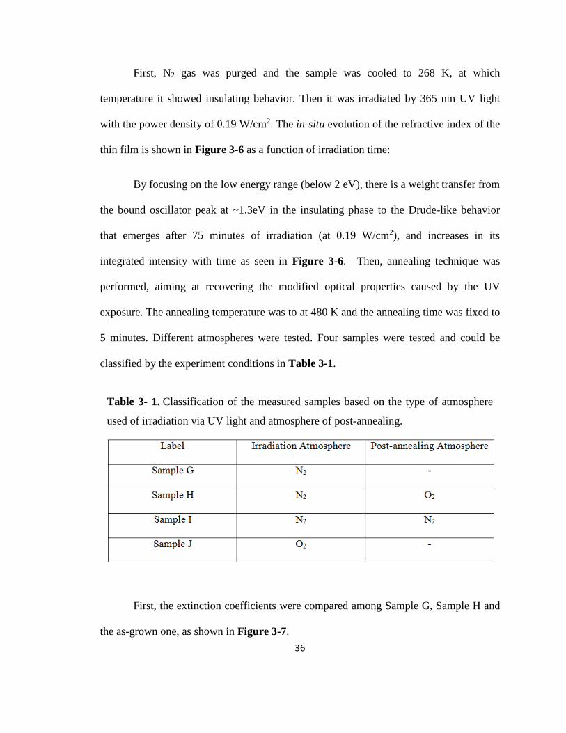
Table 2- 1. Classification of the measured samples based on the type of atmosphere used
of irradiation via UV light and atmosphere of post-annealing. ........................................ 14
Table 2- 2. Carrier concentration, mobility and resistivity values for pristine sample and
the sample irradiated by UV light in N2............................................................................ 19
Table 3- 1. Classification of the measured samples based on the type of atmosphere used
of irradiation via UV light and atmosphere of post-annealing. ........................................ 36
Table 4- 1. The penetration depth of VO2 at different excitation incident wavelength. .. 45
Table B- 1. Details of oscillators used to analyze Spectroscopic Ellipsometry of the
pristine VO2 sample at metallic phase. ............................................................................. 54
Table B- 2. Details of oscillators used to analyze Spectroscopic Ellipsometry of the
pristine VO2 sample at insulating phase. .......................................................................... 54
Table B- 3. Details of oscillators used to analyze Spectroscopic Ellipsometry of the
pristine VO2 sample irradiated by UV in N2 for 25 minutes. ........................................... 55
Table B- 4. Details of oscillators used to analyze Spectroscopic Ellipsometry of the
pristine VO2 sample irradiated by UV in N2 for 50 minutes. ........................................... 55
Table B- 5. Details of oscillators used to analyze Spectroscopic Ellipsometry of the
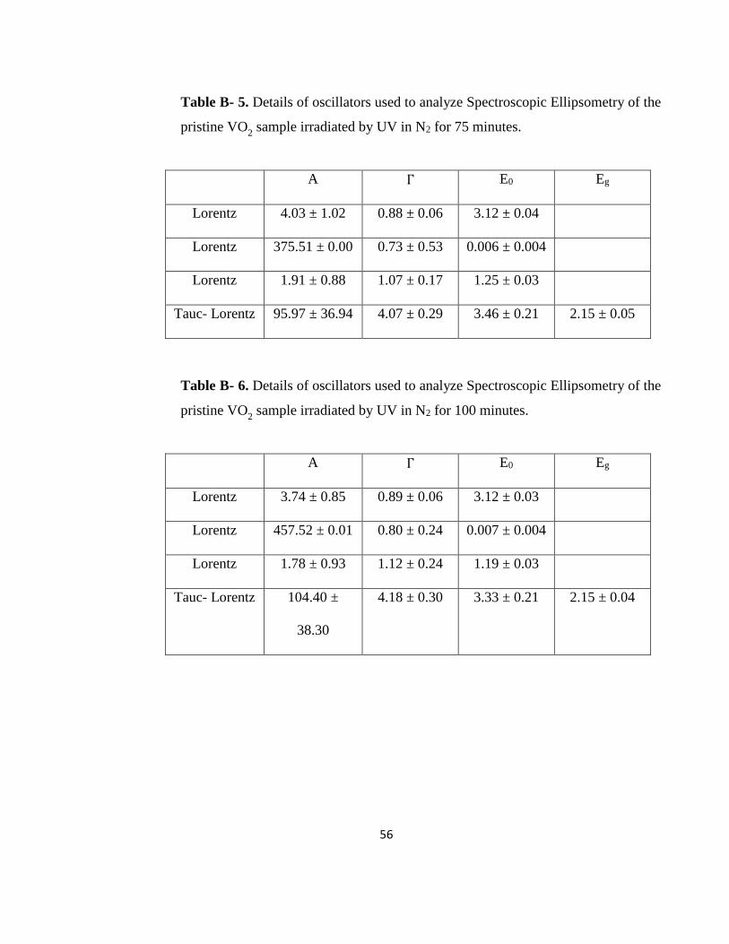
pristine VO2 sample irradiated by UV in N2 for 75 minutes. ........................................... 55
Table B- 6. Details of oscillators used to analyze Spectroscopic Ellipsometry of the
pristine VO2 sample irradiated by UV in N2 for 100 minutes. ......................................... 55
Page 10
x
Table B- 7. Details of oscillators used to analyze Spectroscopic Ellipsometry of the
pristine VO2 sample irradiated by UV in N2 for 125 minutes. ......................................... 55
Table B- 8. Details of oscillators used to analyze Spectroscopic Ellipsometry of the
pristine VO2 sample irradiated by UV in N2 for 150 minutes. ......................................... 55
Table B- 9. Details of oscillators used to analyze Spectroscopic Ellipsometry of the
pristine VO2 sample irradiated by UV in N2 for 175 minutes. ......................................... 55
Table B- 10. Details of oscillators used to analyze Spectroscopic Ellipsometry of the
pristine VO2 sample irradiated by UV in N2 for 200 minutes. ......................................... 55
Table B- 11. Details of oscillators used to analyze Spectroscopic Ellipsometry of the
pristine VO2 sample irradiated by UV in N2 for 225 minutes (Sample G). ...................... 55
Table B- 12. Details of oscillators used to analyze Spectroscopic Ellipsometry of the
pristine VO2 sample irradiated by UV in N2 and the annealed in O2 (Sample H). ........... 55
Table B- 13. Details of oscillators used to analyze Spectroscopic Ellipsometry of the
pristine VO2 sample irradiated by UV in N2 and the annealed in N2 (Sample I). ............ 55
Table B- 14. Details of oscillators used to analyze Spectroscopic Ellipsometry of the
pristine VO2 sample irradiated by UV in O2 (Sample J). ................................................. 55
Page 11
xi
Acknowledgements
I would like to thank Office of Naval Research (ONR) for funding support. With
the support from you, the thesis work is able to perform.
Next, I would like to thank Dr. Venkatraman Gopalan. He is a wise advisor. He
inspired me to design experiments, conduct experiments and analyze data independently.
Thanks for his help suggestions and discussion with me throughout my project. In
addition, I would like to thank Dr. Roman Engel-Herbert and Dr. John V. Badding.
Without guidance and help from them, this thesis work is impossible. I also would like to
thank Materials Research Institute (MRI) in Penn State University. The friendly staff and
advanced equipment provided perfect conditions for performing experiments.
Then I would like to specially thank all my fellow group members, namely Ryan
Haislmaier, Arnab Sen Gupta, Yunzhi Liu, Shiming Lei, Brian Vanleeuwen, Xiaoyu Ji,
Angela Leone, Yakun Yuan, Gregory Aaron Stone, Hirofumi Akamatsu. You helped me
not only in academic field but also in my life. At the same time, I would like to thank the
perfect cooperation from collaborators.
I would like to thank my friends and parents. Thanks for their support during the
past three years. Specially, I would like to thank my friend Chengxi Lu, who spent huge
amount of time and efforts on editing thesis.
I would like to thank the Penn State University. I experienced the most wonderful
three years here in my life.
Page 12
1
Chapter 1 Background
Metal-Insulating Transition (MIT) in strongly correlated systems is one of the
attractive topics in the field of condensed matter physics.[4] MIT is a first order phase
transition and across the transition, the properties of the material such as resistivity,
changes dramatically, by orders of magnitude[5], attracting attention from both the
scientific and the engineering researchers. Theoretical description of the MIT
phenomenon is quite different from the conventional band theory which is based on the
free electron or weak electron-electron interaction assumption. In the conventional band
theory, the highest filled electronic band of metals is partially filled at 0 K, which is
conduction band, while the conduction band for an insulator phase is empty. In other
words, the position of Fermi level lies in the conduction band for metals and in the band
gap for insulators. Though it can depict electronic properties for many materials well,
conventional band theory doesn’t work well on transition metal oxides with partially
filled d- shell electronic band. Instead of good conductors predicted by the classical band
theory, they are usually insulators. The lack of parameters to describe the strong
correlation effect between electrons or between electron and lattice makes the
conventional band theory unsatisfactory. To resolve these disadvantages, the concept of
Mott-Hubbard type and charge transfer type insulators is established, by introducing
parameters such as Coulomb repulsion energy U and charge transfer energy Δ0.[5]
Numerous transition metal oxides display MIT phenomena. In this thesis, vanadium
dioxide (VO2) as one of the prototypical MIT systems was chosen to study.
Page 13
2
VO2 displays structural change from an insulating phase at low temperature to a
metallic phase at high temperature with the decrease in resistivity by as much as 5 orders
of magnitude. Carrier concentration change (~1023 cm-3 in the metallic phase and ~1019
cm-3 in the insulating phase[6]), instead of a change in mobility, explains the change of
resistivity.[7] The structural change occurs at the same time as when the resistivity alters.
Figure 1- 1. Crystal structure of VO2. a) The rutile crystal structure of VO2. b) The
M1 phase structure for monoclinic VO2 below transition temperature. c) The M2
phase structure for monoclinic VO2 below transition temperature. The red balls
represent V atoms and the blue balls represent O atoms.
Page 14
3
In the monoclinic phase, vanadium atoms dimerize and tilt along the c axis in
pairs due to the Peierls distortion.[8] In rutile phase, however, vanadium atoms align along
a line, causing the unit cell to shrink to half of its volume in the monoclinic phase. To be
specific, VO2 with M1 phase below transition temperature undergoes the following
structure evolution across the MIT[7, 9-11], 𝒂𝑴 = 𝟐𝒄𝑹, 𝒃𝑴 = 𝒂𝑹, 𝒄𝑴 = 𝒂𝑹 − 𝒄𝑹 The
lattice constant is 𝑎𝑅 = 𝑏𝑅 = 4.55 Å; 𝑐𝑅 = 2.85 Å; 𝑎𝑀1 = 5.70 Å; 𝑏𝑀1 = 4.55 Å; 𝑐𝑀1 =
5.38 Å; 𝛽𝑀1 = 123°. Subscripts R and M1 refer to rutile and M1 phase, respectively.
The transition from the M2 phase to rutile phase is approximately 𝒃𝑴𝟐 = 𝟐𝒄𝑹,
𝒂𝑴𝟐 = 𝟐𝒂𝑹, 𝒄𝑴𝟐 = −𝒃𝑹 . The lattice constant of M2 phase is 𝑏𝑀2 = 5.80 Å; 𝑎𝑀2 =
9.07 Å; 𝑐𝑀2 = 4.53 Å; 𝛽𝑀2 = 92°.[11] Subscript M2 refers to M2 phase.
Figure 1- 2. The structure evolution of VO2 across MIT, from M1 structure to rutile
structure. The blue frame represents the rutile structure of VO2 above transition
temperature. The red frame represents the monoclinic structure of VO2 below
transition temperature.
Page 15
4
Abundant studies have been conducted on the synthesis methods in order to study the
MIT properties in VO2. Thin film technique is especially important because it provides an
opportunity to understand VO2 on the microscopic scale. The appropriate growth
condition plays a key role in the quality of grown films, such as the growth pressure in
Physical Vapor Deposition methods and the precise control of composition during
synthesis.[9] Molecular Beam Epitaxy (MBE) provides ultrahigh vacuum growth
condition and the ability to control element flux during growth, which make it a very
advanced tool for high quality VO2 thin film synthesis. In our study, the samples are 10
nm VO2 thin films on the TiO2 (001) substrate provided by Dr. Darrell Schlom’s Group
from the Cornell University.[12]
The resistivity versus temperature curve presents the characteristics of MIT
phenomena of VO2. Figure 1-3 shows the hysteresis behavior of 10 nm VO2/TiO2 (001)
thin films studied in this thesis.
Page 16
5
The MIT shows the drop in resistivity up to around 3 orders of magnitude near the
transition temperature (T = 275 K) for the cooling cycle, marked by blue arrow in the
figure. For single crystal bulk VO2, the change can be as high as 5 orders. 4 orders of
resistivity change are observed for epitaxial VO2 films. Meanwhile, hysteresis loop is
observed, which means the heating cycle doesn’t overlap with the cooling cycle. The
width and sharpness of hysteresis loop are mainly determined by the quality, namely
stoichiometry and crystallinity, of the VO2 material. Sharper and narrower hysteresis loop
is the characteristic of high quality thin films. The width of the loop for our sample is
Figure 1- 3. Resistivity vs. temperature for the 10 nm VO2/TiO2 (001) film. The
transition temperature for heating cycle is around 290 K while that for cooling cycle is
around 275 K.
Page 17
6
around 7 K, and the MIT takes place within 0.5 K for one cycle, indicating a sharp
transition. The VO2 ultrathin film we studied is of high quality.
The transition temperature for VO2 thin films can be tuned by the stress. By
utilizing a lattice-mismatched substrate, certain strain can be transferred to the epitaxial
VO2 film on the substrate, therefore uniaxial stress is applied. The transition temperature
for our sample is around 275 K due to 0.86 % tensile strain on the TiO2 (001) substrate,
while that of bulk VO2 is around 340 K. Via controlling such strain, VO2 films display
MIT from down to room temperature to even above the bulk transition temperature.[13, 14]
MIT of VO2 can be triggered not only by heat, but also by other external factors
such as electrical field. When an external field was applied, the dramatic and fast changes
in the resistivity can be utilized to modulate the tunneling current, making VO2 a
promising candidate in temperature-activated switching and optoelectronics, which has
been studied intensively since 1959.[7]
However, the mechanism of the transition is still a highly controversial topic. It
has been debated for a long time whether the electron-electron interaction is strong
enough to localize electrons to form “Mott-Hubbard insulator” or the structure distortion
itself - electron phonon interaction - can trigger the insulating phase, described by Peierls
theory.[15]
The interaction between vanadium oxide and light has been studied for years. A
pulsed laser can trigger the MIT of VO2. This is used in optical pump probe studies to
study the dynamics of phase transition of VO2 with varying temperatures. An example of
Page 18
7
800nm laser with 50mJ/cm2 and 100-fs pulses is used to induce the MIT by promoting
hole photo doping into the valence band of the insulating phase.[16] MIT occurs within the
first 100fs. Moreover, pumped metallic phase recovers to the insulating phase during the
time interval between 2 pulses (repetition rate is 1kHz). Namely, by appropriate power
density, pulsed laser could trigger MIT of VO2. As for continuous wave light, reported
by Ko, the stoichiometry of VO2 films can be modulated by UV exposure (wavelength
used were primarily 185nm and 254nm).[17] Starting from oxygen deficient VO
compounds, UV exposure can enhance the oxidation of films via activated oxygen. The
top surface is oxidized from the beginning, followed by the diffusion-limited oxidizing
process inside the film. In that way, the stoichiometry of VO2 films is modulated by UV-
assisted oxidization. Oxidization is not the only effect from UV exposure on vanadium
oxides. When 405nm UV light is applied at a power density of 20mW/cm2 in air, V2O5
can be reduced into VO2, thus makes V2O5 a candidate for UV photoresist.[18] When small
power density of UV light is used, no modification of stoichiometry is observed and
metal-insulating phase transition is induced on VO2 nanowires, in which 365nm UV is
applied with a power density of 7μW/cm2.[19] Thus, the interaction between light and
VO2 thin film is affected by parameters such as power density and irradiation wavelength.
No systematic study has been conducted on the effect of UV irradiation in different
atmospheres. In our study, we use 365nm UV light for example exposure. Electrical
measurements were performed to characterize transport properties of VO2 thin films,
such as hysteresis loop, carrier concentration and mobility, after UV irradiation occurred.
SIMS was used to clarify the role of oxygen vacancies in MIT modification by UV light.
Optical measurements via spectroscopic ellipsometry were done to characterize optical
Page 19
8
band modification due to UV light exposure. Optical characterization result was then
compared with electrical characterization. Utilizing the ability to manipulate MIT
behavior to avoid modification effect from UV light, UV Raman could be used
appropriately and able to characterize the structure change of VO2 thin films across MIT.
In the last, we propose the future directions of the work.
Page 20
9
Chapter 2 Electrical Characterization of Transport
Properties
Electrical transport measurements reveal the electronic properties of materials,
such as resistivity, carrier concentration and mobility. It is important to characterize
transport properties for VO2 because it exhibits dramatic change in electronic properties
when MIT takes place. To characterize the transport properties of VO2 thin film, two
terminal devices need to be fabricated.
2.1 Two Terminal Devices Fabrication
To prepare the sample for resistivity measurement, conventional Circular
Transmission Line Model (CTLM) pattern was used to fabricate devices. The pristine
sample was first cleaned by aceton, DI water and IPA. After that, 0.5 μm photoresist
LOR 5A layer followed by 1.4 μm photoresist SPR 3012 layer was coated on the VO2
thin film surface via spin coating technique. A 7.7-second exposure under 365 nm UV
light in hard contact mode was then conducted. When the exposure was done, the sample
was dipped into developer solution CD 26 for 60 seconds to remove the remaining
photoresist that didn’t react. Then it was cleaned by DI water and dried by N2. 15 nm Pt
followed by 50 nm Au was deposited at a rate of 0.4 Å/s and 1.5 Å/s, respectively to
fabricate electrodes. Pt was used to prevent gold diffusion into VO2 thin film at high
temperatures. At last, the sample was placed in Remover PG solution for 10 minutes to
remove reacted photoresist and then cleaned by DI water. A bunch of two terminal
devices were fabricated in this process and used in following experiments. One of the
Page 21
10
main advantages of CTML structures is that the current is restricted to flow from the
central contact to the surrounding contact. By applying CTLM, there is no need to etch or
isolate the measured layer comparing to linear Transmission Line Model (TLM)
structures.[20]
2.2 Measurement of the UV Irradiated VO2 Films
Cascade probe station with temperature controller was used to characterize the
transport properties of VO2 thin film. The station can be cooled down to as low as 238 K.
In this study, we focused on the effect of UV irradiation on the transport properties of
VO2 thin film across MIT. The measurement temperature was set from 268 K to 298 K,
with the interval step of 1 K. The schematic set-up for measurement is shown in Figure
2-1.
Page 22
11
The yellow stripes and green circles represented the CTLM pattern. In the
measurement, one probe contacted the inner circle contact, while the other probe
contacted the outside electrode, which was connected to the ground. A sweeping voltage
V from -0.5 V to 0.5 V in the form of rectangular waves was applied, while the current I
was measured. Thus the resistance R of the device could be calculated by the slop of
collected I-V curve. Thus resistivity 𝜌 could be calculated as Eq. 2-1, because of the
geometry of the device and the contact resistance could be ignored:
𝜌 =𝑅∙2𝜋∙(𝑟𝑖𝑛𝑛𝑒𝑟+𝐿
2⁄ )∙𝑡
𝐿 Eq. 2-1
In which, R is the measured resistance; 𝑟𝑖𝑛𝑛𝑒𝑟 is the inner radius of CTLM (60μm in this
case); L is the width of annular gap (6 μm in this study); t is the thickness of the film (10
Figure 2- 1. A schematic diagram of set-up for transport properties characterization.
365 nm UV light was used for irradiation. The inner contact was connected to voltage
source and the outside electrode was connected to the ground.
Page 23
12
nm). 365 nm UV light was shone uniformly from the film of the sample, with a power
density of 0.19 W/cm2. The UV irradiation lasted for 60 minutes and the temperature of
the samples was kept at 278 K during the irradiation. First, the UV irradiation took place
in non-oxidizing atmosphere - N2 - and then the experiment under same condition was
conducted in oxidizing atmosphere - O2. 99.999% N2 and 99.994% O2 were used in the
whole experiments.
When 10 nm VO2/TiO2 (001) was irradiated by UV light in N2, resistivity of the
original insulating region decreased, showing metallic behavior. As seen in Figure 2-2,
Figure 2- 2. Hysteresis loop measurement after UV irradiation in different
atmosphere. UV irradiation was performed on samples in N2 and O2, respectively. The
hysteresis behavior for those two samples and the pristine one were compared. Arrows
marked in the figure indicated the direction for temperature varying.
Page 24
13
the order of magnitude in resistivity change across MIT dropped to 1.5 after irradiation
instead of 2.5 for pristine sample, namely MIT behavior was suppressed by 1 order of
magnitude. Besides, the hysteresis loop displayed a wider transition after irradiation.
In contrast, irradiation was performed under the same condition but in O2
atmosphere. There was no suppression of the MIT; instead the hysteresis increased
somewhat, possibly indicating great defect densities after UV irradiation.
2.3 Measurement of VO2 Films under Different Post-annealing Atmosphere
With irradiation of UV light in N2, metallization was induced within the
insulating phase of the VO2. To explore whether such suppressed MIT could be
recovered, post-annealing studies were performed, afterwards. First, two samples were
irradiated via UV light in N2 in order to suppress its MIT behavior. Post-annealing was
performed at 480 K for 5 minutes. Annealing atmospheres of N2 and O2 were tested
separately. The other two samples were irradiated in O2. Post-annealing experiments
were conducted in N2 and O2 as well. Those samples were classified as below, based on
different experiment procedures, in Table 2-1.
Page 25
14
Hysteresis behavior of all the samples was measured. In Figure 2-3, the hysteresis
loop of Sample A and Sample B were reported, comparing that of the as-grown sample.
After annealing, the resistivity of sample A was still 10 times smaller than that of the as-
grown sample when T < Tc, indicating that the suppression still persisted. Meanwhile, the
width of thermal hysteresis loop became much wider. The resistivity of Sample B
matched that of as-grown sample within all tested temperature range, demonstrating that
the suppressed MIT behavior was recovered.
Table 2- 1. Classification of the measured samples based on the type of atmosphere
used of irradiation via UV light and atmosphere of post-annealing.
Page 26
15
In Figure 2-4, the hysteresis behavior of Sample C and Sample D were reported.
There was no modification of the thermal hysteresis, which demonstrated that thermal
annealing technique didn’t, by itself, affect the MIT characteristics of the VO2 film.
Figure 2- 3. Hysteresis loop for post-annealing in different atmosphere after irradiation
in N2. The hysteresis behavior of Sample A, Sample B and the pristine one were
compared. Arrows marked in the figure indicated the direction for temperature
varying.
Page 27
16
Based on the results above, MIT suppression only takes place in the non-
oxidizing atmosphere and could be recovered in oxidizing atmosphere.
2.4 Hall Measurement of VO2 Thin Films
During the Hall measurement, current is forced through the materials with
magnetic field applied. Hall voltage is generated to compensate the Lorentz Force on
moving carriers in magnetic field then, and is measured in measurement. Figure 2-5
displays an example of the Hall measurement in the VO2 film irradiated in N2 by UV, via
van der Pauw method at 200 K and 320 K. According to the Hall measurement, the main
Figure 2- 4. Hysteresis loop of the samples post-annealed in N2 and O2 atmosphere
for irradiated sample in O2.
Page 28
17
carriers are electrons in VO2. The slopes of Hall voltage versus applied magnetic field in
Figure 2-5 correspond to the carrier concentration, defined by
𝑛 =𝐼∙𝐵𝐻
𝑉𝐻∙𝑒∙𝑡 Eq. 2-2
Where 𝐼 is the current through materials; 𝐵𝐻 is the magnetic field flux perpendicular to
the sample plane; 𝑉𝐻 is the measured Hall voltage; 𝑡 is the thickness of the film which is
10 nm in this study; 𝑒= 1.6 10-19 C. Thus, n (T) can be extracted from temperature-
dependent Hall measurements before and after irradiation in N2.
Figure 2- 5. The Hall voltage in the metallic (blue data points) and insulating (red
data points) phases of the VO2 thin film irradiated by UV light in N2.
Page 29
18
In Figure 2-6, carrier concentration of VO2 films before and after irradiation was
shown from 200 K to 320 K.
Compare it with resistivity change in Figure 2-2. Mobility 𝜇 of carriers is defined
by:
𝜇 = 1/(𝑛𝑒𝜌) Eq. 2-3
280 K is around the temperature where MIT takes place therefore, we focus on
the temperature of 260 K and 300 K; VO2 thin films exhibit stable insulating and metallic
behaviors at those temperatures. Carrier concentration, mobility and resistivity values
were listed in Table 2-2:
Figure 2- 6. Carrier concentration of the VO2 thin film as a function of temperature
before and after UV irradiation in N2 atmosphere.
Page 30
19
Resistivity at 260 K was extrapolated from Figure 2-2. When T = 260 K,
nuv/npristine was ~3.2, 𝜌 uv/ 𝜌 pristine was ~0.13, 𝜇𝑈𝑉/𝜇𝑝𝑟𝑖𝑠𝑡𝑖𝑛𝑒 was ~2.4. Below transition
temperature after irradiation in N2, the increase of carrier concentration mainly accounted
for the resistivity decrease which meanwhile was affected by mobility change. At T =
300 K, nuv/npristine was ~2.2, 𝜌 uv/ 𝜌 pristine was ~0.86, 𝜇𝑈𝑉/𝜇𝑝𝑟𝑖𝑠𝑡𝑖𝑛𝑒 was ~0.5.
The mechanism for this MIT suppression is proposed to be the creation of oxygen
vacancies in the VO2 films by bond breaking under UV irradiation in a non-oxidizing
atmosphere: UV light broke V-O bonds in the thin film resulting in oxygen diffusing out
of VO2 thin films. Thus, oxygen vacancies were left in the films. MIT was suppressed
upon irradiation in non-oxidizing atmosphere. Non-oxidizing atmosphere had lower
concentration of oxygen comparing to that in the film, oxygen was promoted to diffuse
out, generating oxygen vacancies easily under irradiation. On the contrary, MIT
suppression didn’t take place upon irradiation in oxidizing atmosphere. Oxidizing
Table 2- 2. Carrier concentration, mobility and resistivity values for pristine sample
and the sample irradiated by UV light in N2.
Page 31
20
atmosphere prevented oxygen from diffusing out, namely restrained the formation of
oxygen vacancies. Therefore, oxygen vacancies played a key role in suppressing MIT
behavior of VO2 thin films. As for post-annealing experiments to recover suppressed
MIT, annealing in oxidizing atmosphere provided chances for oxygen to diffuse into
suppressed VO2 thin film, compensating oxygen vacancies. Therefore, post annealing in
O2 was successful in suppressed MIT recovery. Oxygen vacancies would increase
scattering effect, thus caused decrease in mobility. From Table 2-2, the decrease of
mobility at 300 K after irradiation could then be understood. In summary, the
stoichiometry and oxygen content in the film after interacting with UV had an influence
on the MIT behavior of VO2.
2.5 Secondary Ion Mass Spectrometry of VO2 Thin Films
In order to directly verify the proposed mechanisms and characterize the vacancy
concentration, 18O2 - the isotopic gas of normal oxygen gas - was used to trace the
existence of oxygen vacancies. Post-annealing in 18O2 was performed for the MIT
suppressed sample. Then if oxygen vacancies were formed before annealing, 18O would
compensate the vacancies during annealing process, leading to an expected increased
signal of 18O within VO2 thin film region, which could be characterized by Secondary Ion
Mass Spectrometry (SIMS) technique.
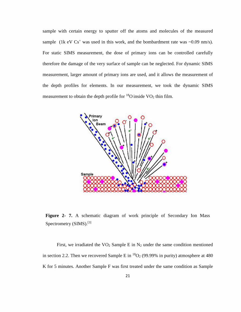
Figure 2-7 shows the schematic diagram of the work principle of SIMS. In SIMS,
charged primary ions beam is focused on the surface of sample and hits the surface of
Page 32
21
sample with certain energy to sputter off the atoms and molecules of the measured
sample (1k eV Cs+ was used in this work, and the bombardment rate was ~0.09 nm/s).
For static SIMS measurement, the dose of primary ions can be controlled carefully
therefore the damage of the very surface of sample can be neglected. For dynamic SIMS
measurement, larger amount of primary ions are used, and it allows the measurement of
the depth profiles for elements. In our measurement, we took the dynamic SIMS
measurement to obtain the depth profile for 18O inside VO2 thin film.
First, we irradiated the VO2 Sample E in N2 under the same condition mentioned
in section 2.2. Then we recovered Sample E in 18O2 (99.99% in purity) atmosphere at 480
K for 5 minutes. Another Sample F was first treated under the same condition as Sample
Figure 2- 7. A schematic diagram of work principle of Secondary Ion Mass
Spectrometry (SIMS).[3]
Page 33
22
E, and then exposed by UV light in N2 again. The second UV irradiation was performed
under the same condition mentioned in section 2.2. SIMS was then used to detect the
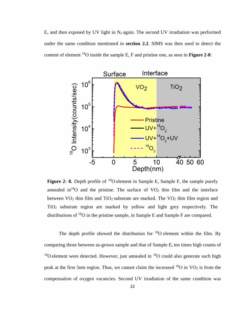
content of element 18O inside the sample E, F and pristine one, as seen in Figure 2-8:
The depth profile showed the distribution for 18O element within the film. By
comparing those between as-grown sample and that of Sample E, ten times high counts of
18O element were detected. However, just annealed in 18O could also generate such high
peak at the first 5nm region. Thus, we cannot claim the increased 18O in VO2 is from the
compensation of oxygen vacancies. Second UV irradiation of the same condition was
Figure 2- 8. Depth profile of 18O element in Sample E, Sample F, the sample purely
annealed in18O and the pristine. The surface of VO2 thin film and the interface
between VO2 thin film and TiO2 substrate are marked. The VO2 thin film region and
TiO2 substrate region are marked by yellow and light grey respectively. The
distributions of 18O in the pristine sample, in Sample E and Sample F are compared.
Page 34
23
performed for the post-annealed one, the profile of 18O element of Sample F shows very
little change in diffusion profile. That demonstrated that UV irradiation didn’t drag out
much 18O from post-annealed VO2 thin film. Thus, oxygen vacancies were formed during
UV irradiation in non-oxidizing atmosphere, but the concentration of it was small.
There are two roles oxygen vacancies could play in affecting the resistivity
properties of VO2 films. For one thing, when one oxygen vacancy is formed, two
electrons are introduced into the system based on the defect chemical equation:
𝑂𝑜× → 𝑉𝑂
∙∙ + 2𝑒 +1
2𝑂2 ↑ Eq. 2-4
The extra electrons could lead to the shift of Fermi Level position[21], and the stabilization
to the metallic phase below the transition temperature. The increase of carrier
concentration after irradiation in Figure 2-6 is a direct proof.
For the other, the existence of oxygen vacancies provided the condition for two
phase intergrowth, resulting in a mixed phases region.[22] Figure 2-8 showed that the
concentration of oxygen vacancy after irradiation was small. However, the increase of
carrier concentration after irradiation in Figure 2-6 reached 3 times higher than that of
pristine. Thus, the increase carriers can not only from free electrons generated with
oxygen vacancies. Mixed phases hypothesis was necessary to explain the role of oxygen
vacancies thoroughly. If metallic phase exists after UV irradiation, according to the
carrier concentration increase across MIT, ~103 higher carrier concentration exists in
metallic region. 𝑓 × 𝑛𝑚𝑒𝑡𝑎𝑙𝑙𝑖𝑐 + (1 − 𝑓) × 𝑛𝑖𝑛𝑠𝑢𝑙𝑎𝑡𝑜𝑟 = 𝑛𝑈𝑉 , in which f is the volume
fraction of metallic pahse, 𝑛𝑚𝑒𝑡𝑎𝑙𝑙𝑖𝑐 , 𝑛𝑖𝑛𝑠𝑢𝑙𝑎𝑡𝑜𝑟 , 𝑛𝑈𝑉 refer to the carrier concentration
Page 35
24
contribution from metallic phase, insulating phase and the carrier concentration after UV
irradiation. 𝑛𝑚𝑒𝑡𝑎𝑙𝑙𝑖𝑐 = ~103 𝑛𝑖𝑛𝑠𝑢𝑙𝑎𝑡𝑜𝑟 𝑎𝑛𝑑 𝑛𝑈𝑉 = 3 𝑛𝑖𝑛𝑠𝑢𝑙𝑎𝑡𝑖𝑛𝑔 .Thus approximately
0.2% of the total volume will be metallic phase. That amount matches the amount of
oxygen vacancies well. Thus, according to the SMIS data, the role of oxygen vacancies is
dominated by the existence of mixed phases.
2.6 Summary
We observed that UV light could cause metallization within the insulating phase
for 10 nm VO2/TiO2 (001) thin film below transition temperature in a non-oxidizing
atmosphere. Annealing in oxygen at 480 K for 5 minutes could recover the MIT of the
VO2 films. The Hall measurement pointed out that modification on resistivity across MIT
after UV exposure mainly came from the change in carrier concentration. Meanwhile,
mobility change also made contribution to the suppression of MIT. Oxygen vacancies
theory was proposed to explain the mechanism of suppression. 18O element was used to
trace the existence of oxygen vacancies directly and further, to measure the concentration
of vacancies. The distribution profile for 18O element within the film measured by SIMS
revealed that the concentration of oxygen vacancies formed during MIT suppression by
UV light was small. More importantly, it pointed out two possible roles of oxygen
vacancies in the suppression. One is to shift the position of Fermi Level by doping
generated free electrons when oxygen vacancies were formed. The other is to create the
condition for existence of mix phases.
Page 36
25
Chapter 3 Optical Characterization of the Band
Structure via Spectroscopic Ellipsometry
3.1 Introduction of the Ellipsometry
Ellipsometry is one of the widely used optical characterizations to analyze the
optical properties of materials. The polarization of the incident light will change after
being reflected from the surface of the sample. This change is described by (𝚿, 𝚫) in the
raw data from an ellipsometer, representing the amplitude ratio 𝚿 and phase difference 𝚫
between incident s- and p-polarized wave. The variables 𝚿 and 𝚫 are defined by[23]
Ρ = tan𝚿 exp(i𝚫) =𝑟𝑝
𝑟𝑠 Eq. 3-1
In which Ρ is a ratio of the amplitude reflection coefficient between s- and p-polarized
light, related to the refractive index of air, measured film, and incident angle. The
polarization change is determined by the structure, composition and optical properties of
the sample. The raw data is then analyzed by optical models with optical oscillators to
obtain those properties of the sample. The optical models contain different layers which
can describe the properties for the substrate, thin film and air. A schematic layer structure
for the model is shown in Figure 3-1. Since the first generation of ellipsometer was
invented by Drude in 1887, various types of ellipsometer have been developed.[23]
Though the ellipsometer with a monochromatic light source is effective enough, a
spectroscopic ellipsometer is used much more widely because the optical properties as a
function of wavelength can be probed within a short time period.[24] Also, the RTSE,
Page 37
26
known as Real-Time Spectroscopic Ellipsometer, has the ability to in-situ the probe
optical band structure and th microstructure non-destructively.[23-26]
In this thesis work, we have learned that the VO2 thin film displays metallization
below the transition temperature after being irradiated by ultra-violet light in non-
oxidizing atmosphere from the electronic measurements in Chapter 2. In Chapter 3, the
optical measurements will be performed to understand this metallization thoroughly.
With the ability to monitor how the metallization evolved with UV irradiation time,
RTSE is the best choice to study the modified MIT of VO2 thin film via UV light.
Figure 3- 1. The structure for optical models used to obtain the refractive index
information. Such model is based of layered air/film/substrate structure.
Page 38
27
3.2 Principle of the Ellipsometry Characterization
The theoretical basis of the ellipsomety describes the interaction between incident
light and the film. Therefore, Maxwell’s Equations need to be introduced to explain this
process. Maxwell’s Equations describe the way of light propagates in both free space and
in a medium. The equations are defined as below (SI units are used):
∇ ∙ 𝐄 =𝜌𝑞
𝜀0 Eq. 3-2
∇ ∙ 𝐁 = 0 Eq. 3-3
∇ × 𝐄 = −∂𝐁
∂t Eq. 3-4
∇ × 𝐁 = 𝜇0 (𝜀0∂𝐄
∂t+ 𝐉) Eq. 3-5
Here E is the electrical field vector; B is the magnetic induction vector; 𝐉 is the vector of
current density. The 𝜌𝑞 represents the charge density and 𝜀0, 𝜇0 are the permittivity and
permeability of free space, respectively. The 𝜀0 , 𝜇0 are constants[27]. When light
propagates into the medium, the permittivity and permeability of the medium need to be
considered. Thus, the electric displacement D and magnetic field vector H are
introduced[28, 29]:
𝐃 = 𝜀0𝜀E̿ Eq. 3-6
𝐁 = 𝜇0�̿�𝐇 Eq. 3-7
Page 39
28
In which 𝜀 ̿and �̿� are the second rank tensors of the permittivity and permeability of the
propagation medium. Taking the isotropic properties of the medium into consideration,
the 𝜀 ̿and �̿� tensor can be reduced to scalar 𝜀 and 𝜇. For simplification, the medium is
treated to be uniform, then 𝜀 and 𝜇 are irrelevant uniform throughout the medium. For
non-magnetic system, 𝜇=1. The refractive index �̃� of materials can be represented by:
𝜀̃ = �̃�2 = 𝜀1 + 𝑖𝜀2 Eq. 3-8
The refractive index �̃� has a complex representation:
�̃� = 𝑛 + 𝑖𝑘 Eq. 3-9
Therefore:
{ 𝜀1 = 𝑛2 − 𝑘2
𝜀2 = 2𝑛𝑘 Eq. 3-10
z axis is chosen as the propagation direction of the light, then the electric field can be
defined as below:
𝚬(𝐫, t) = 𝚬𝟎exp [𝑖𝜔((�̃�𝒛
𝑐) − 𝑡0)] Eq. 3-11
The propagating wave can be expanded as:
𝚬(𝐫, t) = (Ε0𝑥 exp(i𝜓𝑥) 𝒙 + Ε0𝑦 exp(i𝜓𝑦) 𝒚)exp [𝑖𝜔((�̃�𝒛
𝑐) − 𝑡0)] Eq. 3-12
In which Ε0𝑥 and Ε0𝑦 represents the amplitude of electric field along x and y axes,
respectively and 𝜓𝑥, 𝜓𝑦 describe phase factors of the electrical field along x and y axes,
Page 40
29
respectively. Those four parameters define the polarization status of propagating light. In
Figure 3-2, a schematic case of an incident light interacting with the surface of the
sample is shown.
The optical signal can be represented by the Fresnel relationship:
𝑟𝑝 = |𝑟𝑝| exp(𝑖𝜓𝑝) =𝑬𝒑
𝒓
𝑬𝒑𝒊 Eq. 3-13
𝑟𝑠 = |𝑟𝑠| exp(𝑖𝜓𝑠) =𝑬𝒔
𝒓
𝑬𝒔𝒊 Eq. 3-14
Figure 3- 2. A schematic case of an incident light interacting on the surface of the
sample. The superscripts i, r, t represent incident beam, reflection beam and
transmitted beam, respectively. And the subscripts s, p describe s- and p-polarized
wave, respectively.
Page 41
30
In which |𝑟𝑝|, |𝑟𝑠| describe the amplitude for p- and s-polarized beam after reflection. 𝜓𝑝,
𝜓𝑠 describe the phase factor for p- and s-polarized beam after reflection.
Therefore, the complex reflection ratio Ρ can be defined by:
Ρ = tan𝚿 exp(i𝚫) =𝑟𝑝
𝑟𝑠=
|𝑟𝑝|
|𝑟𝑠| exp [𝑖(𝜓𝑝 − 𝜓𝑠 ) Eq. 3-15
tan𝚿=|𝑟𝑝|
|𝑟𝑠| , 𝚫 = 𝜓𝑝 − 𝜓𝑠 Eq. 3-16
𝚿 and 𝚫 in Eq. 3-15 and Eq. 3-16 are the variables measured directly by the ellipsometer.
Those data need to be analyzed by appropriate optical models with optical oscillators to
obtain the optical band and dielectric properties of the materials.
3.3 Optical Properties of VO2 Thin Film
The optical properties of VO2 varies from bulk to thin films, and have been
studied by spectroscopic ellipsometry, from which the optical band information can be
obtained.[30-32] In our study, 10 nm VO2/TiO2 (001) sample was attached to a temperature
controller and was mounted on the base of RC2 instrument (See Appendix A for details).
Measurements were done at 268 K and 300 K. The experimental data was modeled via
CompleteEase Software over the spectral range from 0.75 eV to 5.16 eV. To analyze the
spectra, a parameterized model with three low energy Lorentz oscillators[33, 34] and one
modified Lorentz oscillator - Tauc Lorentz oscillator[34, 35] - was established. Lorentz
oscillator is defined by amplitude A, a broadening Γ and a center energy location E0.
Page 42
31
ε =ΑΓΕ0
Ε02−Ε2−𝑖ΓΕ
Eq. 3-17
For Tauc-Lorentz oscillator, one more parameter representing band gap Eg is necessary
It is defined by:
𝜀2 = {ΑΕ0Γ
(Ε2−Ε02)2+Γ2Ε2 ∙
(Ε−Ε𝑔)2
Ε Ε>Ε𝑔
0 Ε≤Ε𝑔
Eq. 3-18
and
𝜀1 =2
𝜋𝑃 ∫
𝑤𝜀2(𝑤)
𝑤2−Ε2 𝑑𝑤∞
Ε𝑔
Eq. 3-19
Here, P denotes the Cauchy principle values and 𝑤 is frequency.
The optical models are used to analyze how UV light modified the MIT behavior
of VO2 thin film in optical properties. The extracted dielectric function can be written by
a sum of oscillators:
ε(ω) = 𝜀∞ −𝜔𝑛
2
𝜔2+𝑖𝜔𝜔𝑐+ ∑
𝑆𝑖
1−𝜔2
𝜔𝑖2−𝑖𝛾𝑖
𝜔
𝜔𝑖
𝑛𝑖=1 Eq. 3-20
In which ε∞ represents the contribution to the real part of dielectric constant from the
high energy transition, the second term in the right hand describes the absorption from
free carriers in the system, where ωn2 corresponds to plasma frequency and ωc is used to
describe the collision frequency[30]. The last term in the equation represents a summation
of different Lorentzian oscillators in the film. All the detailed information about
Page 43
32
oscillators is listed in Appendix B. For as-grown sample, which is the reference, the
obtained dielectric properties are shown in Figure 3-3 (parameters for oscillators used in
the analysis are listed in Table B-1 in the Appendix B):
At T = 268 K, the film showed insulating properties indicated by the peak located
at the 1.2 eV, shown in Figure 3-3b. At T = 300 K, the film exhibits metallic properties,
indicated by the dramatic rise of Drude-like tail below 2 eV, seen as Figure 3-3a. The
imaginary part of the refractive index, extinction coefficient, derived from dielectric
Figure 3- 3. The dielectric constant as a function of photon energy for the epitaxial
10nm VO2/TiO2 (001) at T < Tc (268 K) and at T > Tc (300 K). Dash line displays the
oscillators used in analyzing raw data to obtain dielectric constant.
Page 44
33
constant, directly reflects the structure of the optical band. In the following study, we
focus on the properties change in extinction coefficient for different samples.
The peaks at 1.2 eV and 3.2 eV in Figure 3-3b correspond to the optical
transitions from filled lower 𝑎1𝑔 band to the empty 𝑒𝑔𝜋 band and from the filled 𝑂2𝑝 band
to empty 𝑒𝑔𝜋 band, respectively, shown in Figure 3-4. The peak at 3.1 eV in Figure 3-3b
corresponds to the optical transitions from the 𝑂2𝑝 bands to partially filled 𝑒𝑔𝜋 bands. The
fluctuation of the peak position around 3.1 eV across metal-insulating transition could be
explained by strong electronic correlation. [31, 36]
𝑎1𝑔
𝑒𝑔𝜎
𝑒𝑔𝜋
𝑎1𝑔
𝑂2𝑝 𝑂2𝑝
𝑎1𝑔
𝑒𝑔𝜋
𝑒𝑔𝜎
𝐸𝐹 𝐸𝐹
Figure 3- 4. The schematic diagram for the band structure of VO2.[1] Regions with
different colors represent different bands, marked at the side. The color arrows
describe certain optical transition between bands. EF shows the position where Fermi
Level lies.
Page 45
34
3.4 Experimental Set-up of Ellipsometry Characterization
The film was attached to the temperature controller and then mounted on the base
of the RC2 instrument. The configuration is shown in Figure 3-5.
UV exposures under different atmosphere were conducted in this experiment to
study the modification effect on optical properties across MIT of VO2. Various gases (N2
and O2) were purged inside the heating stage as shown in Figure 3-5b. Figure 3-5c
Figure 3- 5 a. The schematic diagram of the set up for insitu monitoring how UV
irradiation modified the MIT of VO2 via Spectroscopic Ellipsometry. b. The photo of
Instec heating stage. c. The design diagram of the cover of the Instec (Unit: inch).
Grey area represents the angel holes in the cover.
Source
Page 46
35
shows the cover design diagram. The angel holes allow the incident beam in and the
reflected beam out. Due to the geometry of the holes in the stage cover, the incident
angle can vary from 67º to 73º.
3.5 Measurement of UV Irradiated VO2 Films and Post-annealed VO2 Films under
Different Atmosphere
The incident angle was set at 70º. The refractive index (raw data) as a function of
UV exposure time could be monitored via RTSE.
Figure 3- 6. The extinction coefficient of 10 nm VO2/TiO2 (001) thin film irradiated
by 365 nm as a function of exposure time. Different lines represent the extinction
coefficient after different exposure time.
Page 47
36
First, N2 gas was purged and the sample was cooled to 268 K, at which
temperature it showed insulating behavior. Then it was irradiated by 365 nm UV light
with the power density of 0.19 W/cm2. The in-situ evolution of the refractive index of the
thin film is shown in Figure 3-6 as a function of irradiation time:
By focusing on the low energy range (below 2 eV), there is a weight transfer from
the bound oscillator peak at ~1.3eV in the insulating phase to the Drude-like behavior
that emerges after 75 minutes of irradiation (at 0.19 W/cm2), and increases in its
integrated intensity with time as seen in Figure 3-6. Then, annealing technique was
performed, aiming at recovering the modified optical properties caused by the UV
exposure. The annealing temperature was to at 480 K and the annealing time was fixed to
5 minutes. Different atmospheres were tested. Four samples were tested and could be
classified by the experiment conditions in Table 3-1.
First, the extinction coefficients were compared among Sample G, Sample H and
the as-grown one, as shown in Figure 3-7.
Table 3- 1. Classification of the measured samples based on the type of atmosphere
used of irradiation via UV light and atmosphere of post-annealing.
Page 48
37
The Drude-like feature is seen after irradiation in N2, which disappears after
annealing in O2. The loss of Drude tail indicates that metallization didn’t exist and that
the insulating properties was recovered after annealing in O2.
After that, annealing in non-oxidizing atmosphere - N2 - was done. The extinction
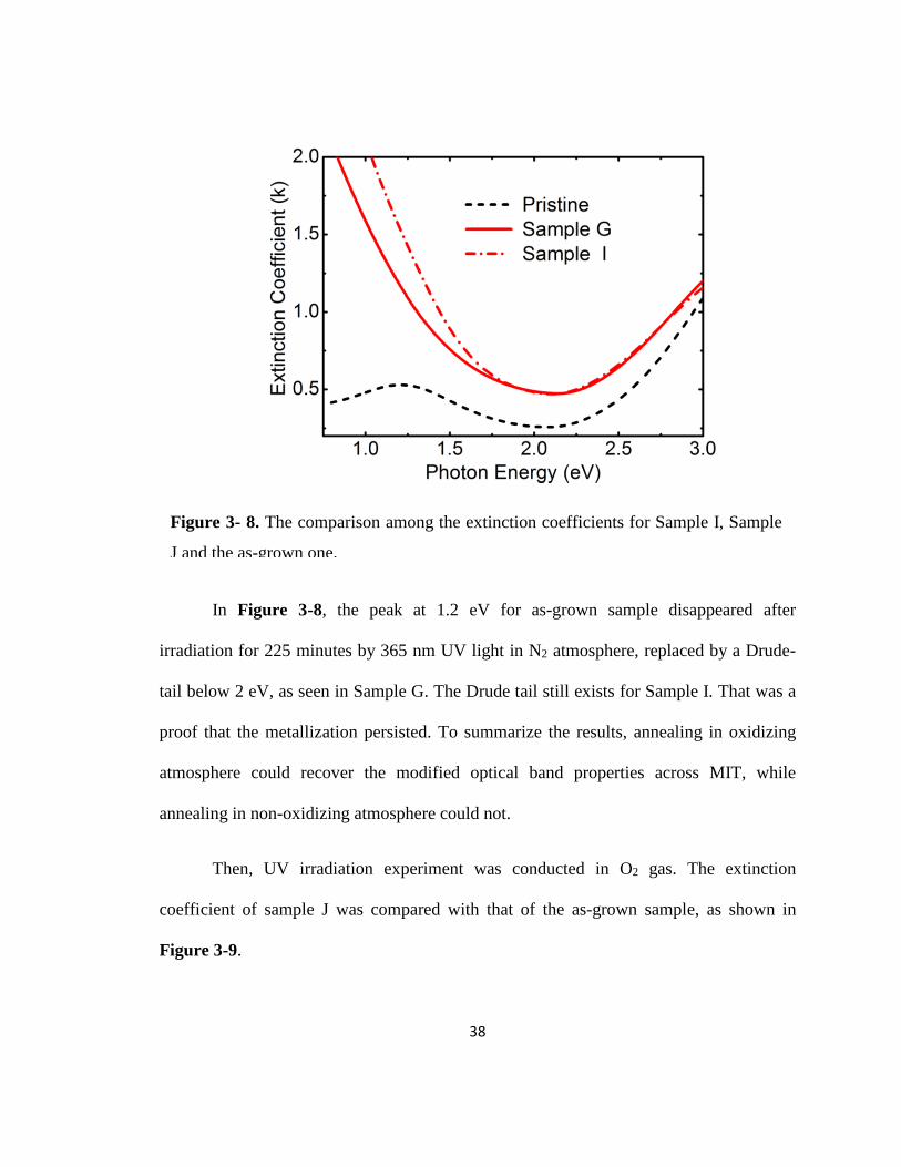
coefficients were compared among Sample G, Sample I and the as-grown one, as shown
in Figure 3-8.
Figure 3- 7. The comparison among the extinction coefficients for Sample G, Sample
H and the as-grown one respectively.
Page 49
38
In Figure 3-8, the peak at 1.2 eV for as-grown sample disappeared after
irradiation for 225 minutes by 365 nm UV light in N2 atmosphere, replaced by a Drude-
tail below 2 eV, as seen in Sample G. The Drude tail still exists for Sample I. That was a
proof that the metallization persisted. To summarize the results, annealing in oxidizing
atmosphere could recover the modified optical band properties across MIT, while
annealing in non-oxidizing atmosphere could not.
Then, UV irradiation experiment was conducted in O2 gas. The extinction
coefficient of sample J was compared with that of the as-grown sample, as shown in
Figure 3-9.
Figure 3- 8. The comparison among the extinction coefficients for Sample I, Sample
J and the as-grown one.
Page 50
39
The peak at 1.2 eV still existed for Sample J. That demonstrates that the optical
transition between VO2 filled lower 𝑎1𝑔 band to the empty 𝑒𝑔𝜋 band does not change by
the UV irradiation. Therefore the thin film still behaves as an insulator and the
metallization didn’t occur. The observations above could be explained by the effect of
oxygen vacancy. Non-oxidizing atmosphere promoted the formation of oxygen vacancies
mechanism by UV irradiation. These results agreed with the previous hysteresis
measurements (shown in Figure 2-3, Figure 2-4, and Figure 2-5) very well.
Figure 3- 9. The comparison between the extinction coefficients between Sample J
and that of as-grown one.
Page 51
40
3.6 Summary
In summary, 365 nm UV light irradiation on VO2 thin film in non-oxidizing
atmosphere caused the merge of 𝑎1𝑔 band and the overlap between 𝑎1𝑔 band and 𝑒𝑔𝜋
band below transition temperature. After irradiation, the Fermi Level position changed to
the middle of 𝑎1𝑔 band, from the gap between 𝑎1𝑔 band and 𝑒𝑔𝜋 band. Thus, the metallic
feature appears after UV irradiation in a reducing atmosphere. However, the UV
irradiation in an oxidizing atmosphere doesn’t change the optical band structure below
the transition temperature. Moreover, annealing in oxidizing atmosphere for samples with
suppressed MIT could recover the optical band structure of VO2 thin film, meaning the
𝑎1𝑔 band splits again and the overlap between 𝑎1𝑔 band and 𝑒𝑔𝜋 band disappears.
Therefore, below the transition temperature, the insulating band structure was recovered.
However, annealing in non-oxidizing atmosphere after thin film irradiated by UV, didn’t
recover the band structure. Combine the above discussion with transport properties
change due to the UV irradiation (discussed in Chapter 2), oxygen vacancies formed
during the UV irradiation is believed to lead to the metallization within the insulating
region of VO2 thin film.
Page 52
41
Chapter 4 Raman Characterization of Films
4.1 Introduction
Scattering happens when light interacts with medium. Based on whether the
conservation of energy is obeyed during the scattering process, there are two types of
processes: elastic scattering where energy is conserved during scattering and inelastic
scattering where energy doesn’tt conserve. Therefore, for elastic scattering, the scattered
light and the incident beam have the same energy (frequency). The elastic scattering is
known as the Rayleigh process, discovered by Rayleigh.[37] In 1923, Adolf Smekal
predicted the inelastic scattering process first[38]. Meanwhile, C.V.Raman, an Indian
scientist, published a series of work on the inelastic scattering effect, which directly led to
the invention of the Raman technique.[39] Figure 4-1 shows a schematic diagram of the
scattering process during light interaction with materials. Raman effect is an inelastic
scattering processes. Therefore, a shift in frequency is generated for the scattered light as
compared to that of incident beam. Raman spectroscopy takes advantage of such
frequency shift, which refers to the required energy difference between the excited
vibrational modes and the ground state.
Page 53
42
Light will be absorbed when propagating into the medium. Without energy
conservation taking place, it is called virtual absorption and the final state is a virtual
state. In the Raman process, incident photon generates oscillating electronic polarization
and which will excite the molecules in the medium to an intermediate state with higher
energy. Subsequently, the higher virtual status molecule will relax to the lower status,
emitting photons at the same time[40]. Such intermediate state can be either a stationary
state or virtual state. The oscillating polarization is able to couple with the polarization
state of the molecules inside the medium, related to the vibrational and electronic excited
state. Therefore, Raman spectrum can be used to observe and study the vibrational
properties of materials. Moreover, Raman active mode can only exist when the derivative
of polarization with atomic coordinate is non-zero.[41] In the spectrum for scattering
radiation, the new energy scattered light are named Raman lines or Raman bands. There
Figure 4- 1. A schematic diagram corresponding to the different types of scattering.[2]
Page 54
43
are two types of Raman lines: one is named Stokes line, corresponding to a lower energy
of emitted photon compared to incident photon, namely the medium absorbs energy; and
the other is named anti-Stokes line, referring to a higher energy of emitted photon,
resulting energy loss in the medium. In the Raman spectrum, the intensity of the scattered
light is displayed as a function of its energy difference with the incident light. Stokes and
anti-Stokes lines locate symmetrically for center point (Δν = 0, where corresponds to the
Relay scattering). That is because they represent the energy difference between the same
upper and lower states. Raman spectrum has been widely used in the study of the
structural change across metal-insulating phase transition of VO2. VO2 displays the space
group of P42/mnm at metallic state[42] and P21/c and, C2/m for the M1 and M2
monoclinic phases respectively.[9] According to group theories and previous studies[9, 43,
44], in insulating phase, there are 9 active Ag and 9 active Bg Raman modes for M1 phase,
and 10 active Ag and 8 active Bg modes for M2 phase. For high temperature metallic
phase, only 1A1g, 1B1g, 1B2g and 1Eg Raman modes exist. In the Raman spectrum,
metallic VO2 shows a broad feature with width larger than 100 cm-1 instead of a sharp
split peaks for insulating VO2.[9] Therefore, different positions of Raman peaks for
insulating phase and metallic phase of VO2 make Temperature-dependent Raman
Spectroscopy an effective technique to probe the structural and phase change across
MIT.[44, 45]
Page 55
44
4.2 UV Raman Experiments, Results and Discussion
First, 16 nm VO2/TiO2 (001) film grown via molecular beam epitaxy was attached
to the Instec stage. 514 nm excitation laser was used in the experiment. The transition
temperature for this sample was around 280 K. Temperature-dependent Raman spectrum
was collected from 253 K to 293 K, with the interval step of 10 K. The series of spectrum
was shown in Figure 4-2. And intentional offset was set for the series of spectrum to
display clearly.
The Raman peaks at 445 cm-1 and 605 cm-1 corresponded to Raman signal from
TiO2 (001) substrate[8], labeled in Figure 4-2. When the temperature was varied across
the MIT temperature, the Raman peaks positions didn’t change. Since the thickness of the
Figure 4- 2. Temperature-dependent Raman Spectrum for VO2/TiO2 (001) thin
film. The temperature increased from 253 K to 293 K, with the internal step of 10
K. Excitation laser wavelength was 514 nm.
Eg
A1g
Page 56
45
sample was too thin, most of the excitation laser penetrated through the thin film and
sampled the substrate. Therefore, the Raman signal from VO2 thin film was too small to
observe. TiO2 (001) substrate dominated the primary Raman signal, and doesn’t display a
phase transition at 280 K. Based on the dielectric constant calculated from Chapter 3, the
penetration depth (defined as the depth where the power of the incident light has
decreased to 1
𝑒2, for VO2) at different incident wavelength is listed in Table 4-1:
Therefore, at 514 nm incident light, the Raman signal in the spectrum was
dominated by the substrate. The signal from film was hard to observe. By comparing the
penetration depth for different incident waves, at 257 nm, least light propagated into the
substrate, leading to most signal from thin film. UV Raman with excitation laser of
257nm in wavelength was chosen. The power density is 2210 W/cm2. And the result is
shown in Figure 4-3. When the experiment underwent, dry N2 was purged to avoid
condensation problem.
Table 4- 1. The penetration depth of VO2 at different excitation incident wavelength.
Page 57
46
The peaks around 600 cm-1 and 820 cm-1 are the peaks of TiO2 substrate. From
253 K to 297 K, the film remains metallic. Based on the analysis from Chapter 2 and
Chapter 3, metallization takes place when VO2 is exposed under UV light in a non-
oxidizing atmosphere. That is to say, the 257 nm excitation laser was able to suppress the
MIT of VO2 thin film leading to no Raman peak position change across the MIT of the
VO2. Moreover, previous chapters also suggest that an oxidizing atmosphere could avoid
the modification of MIT. In the following experiments, O2 was purged to prevent MIT
modification via UV light. 10nm VO2/TiO2 (001) sample was measured from 223 K to
298 K. The spectrum was displayed in Figure 4-4. Offset of each spectrum is set
manually for clear display.
Figure 4- 3. Temperature-dependent UV Raman Spectrum for 10 nm VO2/TiO2
(001) thin film. Temperature varies from 253 K to 297 K. Excitation laser
wavelength is 257 nm. Dry N2 is purged during cooling process.
TiO2 A1g TiO2 B2g VO2 Ag
Page 58
47
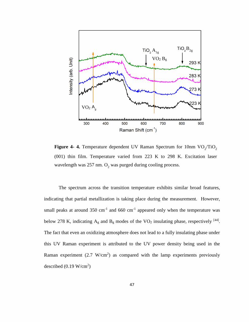
The spectrum across the transition temperature exhibits similar broad features,
indicating that partial metallization is taking place during the measurement. However,
small peaks at around 350 cm-1 and 660 cm-1 appeared only when the temperature was
below 278 K, indicating Ag and Bg modes of the VO2 insulating phase, respectively [44].
The fact that even an oxidizing atmosphere does not lead to a fully insulating phase under
this UV Raman experiment is attributed to the UV power density being used in the
Raman experiment (2.7 W/cm2) as compared with the lamp experiments previously
described (0.19 W/cm2)
Figure 4- 4. Temperature dependent UV Raman Spectrum for 10nm VO2/TiO
2
(001) thin film. Temperature varied from 223 K to 298 K. Excitation laser
wavelength was 257 nm. O2 was purged during cooling process.
A1g
B2g
VO2
VO2 Bg
Page 59
48
4.3 Summary
In summary, due to the small penetration depth for Raman with visible excitation
laser, the signal from thin film is too small to observe the MIT behavior with temperature
increasing or decreasing. UV Raman with 257 nm excitation laser can give us the
smallest penetration depth and the best thin film signal. Under a reducing atmosphere, the
UV laser in UV Raman suppresses the MIT of VO2 thin film; leading to metallic
properties of the film even when the temperature is below the transition temperature.
Based on the findings in the previous chapters, the oxidizing atmosphere could solve the
suppression problem, providing us chance to monitor the MIT process for ultrathin VO2
film on TiO2 (001) substrate. Results showed that the Raman peaks at 660 cm-1 appeared
below the transition temperature, matching one of the Bg modes in insulating phase. That
proves that it is possible to monitor the MIT of ultrathin VO2 film on TiO2 (001) via UV
Raman. However, the main feature of Raman spectrum remained broad and unchanged,
indicating partial suppression still existing because of the much higher density of the UV
laser being used. In the future, oxygen flow and UV excitation power density need to be
optimized aiming at showing a sharp change in the Raman spectrum across the MIT.
Page 60
49
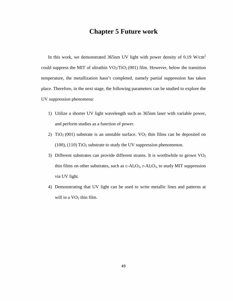
Chapter 5 Future work
In this work, we demonstrated 365nm UV light with power density of 0.19 W/cm2
could suppress the MIT of ultrathin VO2/TiO2 (001) film. However, below the transition
temperature, the metallization hasn’t completed, namely partial suppression has taken
place. Therefore, in the next stage, the following parameters can be studied to explore the
UV suppression phenomena:
1) Utilize a shorter UV light wavelength such as 365nm laser with variable power,
and perform studies as a function of power.
2) TiO2 (001) substrate is an unstable surface. VO2 thin films can be deposited on
(100), (110) TiO2 substrate to study the UV suppression phenomenon.
3) Different substrates can provide different strains. It is worthwhile to grown VO2
thin films on other substrates, such as c-Al2O3, r-Al2O3, to study MIT suppression
via UV light.
4) Demonstrating that UV light can be used to write metallic lines and patterns at
will in a VO2 thin film.
Page 61
50
Reference
1. Eyert, V., The metal-insulator transitions of VO2: A band theoretical approach.
arXiv preprint cond-mat/0210558, 2002.
2. http://www.nt.ntnu.no/users/floban/KJ%20%203055/Surface/SIMS.htm
3. http://en.wikipedia.org/wiki/Raman_spectroscopy
4. Wen, H., et al., Structural and electronic recovery pathways of a photoexcited
ultrathin VO 2 film. Physical Review B, 2013. 88(16): p. 165424.
5. Imada, M., A. Fujimori, and Y. Tokura, Metal-insulator transitions. Reviews of
Modern Physics, 1998. 70(4): p. 1039.
6. Berglund, C. and H. Guggenheim, Electronic Properties of V O 2 near the
Semiconductor-Metal Transition. Physical Review, 1969. 185(3): p. 1022.
7. Zylbersztejn, A. and N. Mott, Metal-insulator transition in vanadium dioxide.
Physical Review B, 1975. 11(11): p. 4383.
8. Qazilbash, M.M., et al., Electrodynamics of the vanadium oxides V O 2 and V 2 O
3. Physical Review B, 2008. 77(11): p. 115121.
9. Petrov, G., V. Yakovlev, and J. Squier, Raman microscopy analysis of phase
transformation mechanisms in vanadium dioxide. Applied physics letters, 2002.
81(6): p. 1023-1025.
10. Goodenough, J.B., The two components of the crystallographic transition in VO<
sub> 2</sub>. Journal of Solid State Chemistry, 1971. 3(4): p. 490-500.
11. Marezio, M., et al., Structural Aspects of the Metal-Insulator Transitions in Cr-
Doped V O 2. Physical Review B, 1972. 5(7): p. 2541.
12. Tashman, J., et al., Epitaxial Growth of VO $ _ {2} $ by Periodic Annealing.
arXiv preprint arXiv:1310.5021, 2013.
13. Ramanathan, S., Thin Film Metal-Oxides: Fundamentals and Applications in
Electronics and Energy. 2009: Springer.
14. Gu, Y., et al., Thermodynamics of strained vanadium dioxide single crystals.
Journal of Applied Physics, 2010. 108(8): p. 083517-083517-7.
15. Gatti, M., et al., Understanding correlations in vanadium dioxide from first
principles. Physical review letters, 2007. 99(26): p. 266402.
16. Cavalleri, A., et al., Evidence for a structurally-driven insulator-to-metal
transition in VO 2: A view from the ultrafast timescale. Physical Review B, 2004.
70(16): p. 161102.
17. Ko, C. and S. Ramanathan, Effect of ultraviolet irradiation on electrical
resistance and phase transition characteristics of thin film vanadium oxide.
Journal of Applied Physics, 2008. 103(10): p. 106104-106104-3.
18. Putrolaynen, V., et al., UV patterning of vanadium pentoxide films for device
applications. Journal of Physics D: Applied Physics, 2007. 40(17): p. 5283.
19. Wu, J.M. and L.B. Liou, Room temperature photo-induced phase transitions of
VO2 nanodevices. Journal of Materials Chemistry, 2011. 21(14): p. 5499-5504.
20. Schroder, D.K., Semiconductor Material and Device Characterization. 2006:
Wiley.
Page 62
51
21. Singh, G., V. Tiwari, and P. Gupta, Role of oxygen vacancies on relaxation and
conduction behavior of KNbO3 ceramic. Journal of Applied Physics, 2010.
107(6): p. 064103.
22. Katzke, H., P. Toledano, and W. Depmeier, Theory of morphotropic
transformations in vanadium oxides. Physical Review B, 2003. 68(2): p. 024109.
23. Fujiwara, H., Spectroscopic ellipsometry: principles and applications. 2007: John
Wiley & Sons.
24. Vedam, K., Spectroscopic ellipsometry: a historical overview. Thin solid films,
1998. 313: p. 1-9.
25. Walker, J., et al., Electronic and structural properties of molybdenum thin films
as determined by real-time spectroscopic ellipsometry. Applied Physics Letters,
2009. 94(14): p. 141908.
26. Hu, Z., et al., Microstructural and optical investigations of sol–gel derived
ferroelectric BaTiO< sub> 3</sub> nanocrystalline films determined by
spectroscopic ellipsometry. Physics Letters A, 2008. 372(24): p. 4521-4526.
27. Griffiths, D.J. and R. College, Introduction to electrodynamics. Vol. 3. 1999:
prentice Hall Upper Saddle River, NJ.
28. Collins, R.W. and K. Vedam, Optical properties of solids. Encyclopedia of
Applied Physics, 1995. 12: p. 285.
29. Wooten, F., Optical properties of solids. Vol. 111. 1972: Academic press New
York.
30. Verleur, H.W., A. Barker Jr, and C. Berglund, Optical Properties of V O 2
between 0.25 and 5 eV. Physical Review, 1968. 172(3): p. 788.
31. Kana Kana, J., et al., Thermally tunable optical constants of vanadium dioxide
thin films measured by spectroscopic ellipsometry. Optics Communications, 2011.
284(3): p. 807-812.
32. Parker, J.C., et al., Optical Properties of the Vanadium Oxides VO2 and V2O5.
Journal of the American Ceramic Society, 1990. 73(11): p. 3206-3208.
33. Tompkins, H. and E.A. Irene, Handbook of ellipsometry. 2005: William Andrew.
34. Jellison Jr, G. and F. Modine, Parameterization of the optical functions of
amorphous materials in the interband region. Applied Physics Letters, 1996.
69(3): p. 371-373.
35. Jellison Jr, G., Spectroscopic ellipsometry data analysis: measured versus
calculated quantities. Thin solid films, 1998. 313: p. 33-39.
36. Qazilbash, M.M., et al., Mott transition in VO2 revealed by infrared spectroscopy
and nano-imaging. Science, 2007. 318(5857): p. 1750-1753.
37. Rayleigh, J.W.S.B., On the Light from the Sky: Its Polarization and Colour. 1870.
38. Smekal, A., Zur quantentheorie der dispersion. Naturwissenschaften, 1923.
11(43): p. 873-875.
39. Raman, C.V., A new radiation. Indian Journal of physics, 1928. 2: p. 387-398.
40. Long, D.A. and D. Long, Raman spectroscopy. Vol. 206. 1977: McGraw-Hill
New York.
41. Shuker, R. and R.W. Gammon, Raman-scattering selection-rule breaking and the
density of states in amorphous materials. Physical Review Letters, 1970. 25: p.
222-225.
Page 63
52
42. Srivastava, R. and L. Chase, Raman spectrum of semiconducting and metallic
VO2. Physical Review Letters, 1971. 27: p. 727-730.
43. Alajtal, A., et al., The effect of laser wavelength on the Raman Spectra of
phenanthrene, chrysene, and tetracene: Implications for extra-terrestrial
detection of polyaromatic hydrocarbons. Spectrochimica Acta Part A: Molecular
and Biomolecular Spectroscopy, 2010. 76(1): p. 1-5.
44. Kim, H.-T., et al., Raman study of electric-field-induced first-order metal-
insulator transition in VO 2-based devices. Applied Physics Letters, 2005. 86(24):
p. 242101-242101-3.
45. Sohn, J.I., et al., Stress-induced domain dynamics and phase transitions in
epitaxially grown VO2 nanowires. Nanotechnology, 2012. 23(20): p. 205707.
46. Motyka, M.A., Effects of microstructure and oxidation state of multi-valent
vanadium oxide thin films for use in infrared microbolometers. 2012.
Page 64
53
Appendix
A. Introduction to RC2 Instrument:
The multichannel, dual-rotating compensator RC2 spectroscopic ellipsometer from J.A.
Woollam Company is used in our study. The set-up is shown in Figure 3-2. This
ellipsometer uses 2 lamps as light sources: a Xe lamp and a Quartz Tungsten Halogen
lamp. Combining these two lamps, the instrument could generate the spectrum ranging
from 0.75 eV to 5.15 eV. The stepper motors control the height of the base stage and the
incident light angle. The height of stage could be varied within 19 mm and the incident
angle could be changed from 45o to 90o. The detector of the instrument is Si-CCD and
InAsGa detector.[46]
Sample stage
Light source Detector
Control box
Figure A- 1. The set-up of the multichannel dual-rotating compensator spectroscopic
ellipsometer
Page 65
54
B. Details of oscillators used in Chapter 3
1. To extract dielectric constant of the pristine VO2 sample, oscillators details are
as below:
A Γ E0 Eg
Lorentz 3.12 ± 0.17 1.28 ± 0.04 3.11 ± 0.01
Lorentz 3.30 ± 1.83 1.65 ± 0.07 0.92 ± 0.17
Tauc- Lorentz 126.34 ± 3.35 5.72 ± 0.14 3.21 ± 0.06 2.03 ± 0.02
One more Drude model was used whose resistivity is 0.003 ± 2.110-5 Ω cm and
scattering time is 1.62 ± 0.3 fs.
A Γ E0 Eg
Lorentz 4.70 ± 1.54 0.95 ± 0.06 3.16 ± 0.04
Lorentz 258.04 ± 0.00 1.43 ± 2.12 0.004 ± 0.005
Lorentz 2.04 ± 0.98 0.98 ± 0.15 1.29 ± 0.02
Tauc- Lorentz 87.10 ± 37.17 4.36 ± 0.34 3.59 ± 0.26 2.08 ± 0.05
Table B- 1. Details of oscillators used to analyze Spectroscopic Ellipsometry of the
pristine VO2 sample at metallic phase.
Table B- 2. Details of oscillators used to analyze Spectroscopic Ellipsometry of the
pristine VO2 sample at insulating phase.
Page 66
55
2. Details of oscillators used to extract the extinction coefficient in Figure 3-6:
A Γ E0 Eg
Lorentz 4.64 ± 1.37 0.96 ± 0.06 3.16 ± 0.04
Lorentz 260.58 ± 0.00 0.87 ± 0.53 0.004 ± 0.005
Lorentz 2.13 ± 0.98 1.03 ± 0.14 1.29 ± 0.02
Tauc- Lorentz 92.18 ± 38.83 4.36 ± 0.33 3.56 ± 0.25 2.12 ± 0.05
A Γ E0 Eg
Lorentz 4.40 ± 1.26 0.97 ± 0.06 3.13 ± 0.03
Lorentz 294.78 ± 0.00 0.80 ± 0.39 0.005 ± 0.005
Lorentz 2.10 ± 0.98 1.05 ± 0.15 1.28 ± 0.03
Tauc- Lorentz 94.18 ± 39.25 4.19 ± 0.31 3.52 ± 0.24 2.14 ± 0.05
Table B- 3. Details of oscillators used to analyze Spectroscopic Ellipsometry of the
pristine VO2 sample irradiated by UV in N2 for 25 minutes.
Table B- 4. Details of oscillators used to analyze Spectroscopic Ellipsometry of the
pristine VO2 sample irradiated by UV in N2 for 50 minutes.
Page 67
56
A Γ E0 Eg
Lorentz 4.03 ± 1.02 0.88 ± 0.06 3.12 ± 0.04
Lorentz 375.51 ± 0.00 0.73 ± 0.53 0.006 ± 0.004
Lorentz 1.91 ± 0.88 1.07 ± 0.17 1.25 ± 0.03
Tauc- Lorentz 95.97 ± 36.94 4.07 ± 0.29 3.46 ± 0.21 2.15 ± 0.05
A Γ E0 Eg
Lorentz 3.74 ± 0.85 0.89 ± 0.06 3.12 ± 0.03
Lorentz 457.52 ± 0.01 0.80 ± 0.24 0.007 ± 0.004
Lorentz 1.78 ± 0.93 1.12 ± 0.24 1.19 ± 0.03
Tauc- Lorentz 104.40 ±
38.30
4.18 ± 0.30 3.33 ± 0.21 2.15 ± 0.04
Table B- 5. Details of oscillators used to analyze Spectroscopic Ellipsometry of the
pristine VO2 sample irradiated by UV in N2 for 75 minutes.
Table B- 6. Details of oscillators used to analyze Spectroscopic Ellipsometry of the
pristine VO2 sample irradiated by UV in N2 for 100 minutes.
Page 68
57
A Γ E0 Eg
Lorentz 3.46 ± 0.30 0.88 ± 0.05 3.11± 0.01
Lorentz 3.05 ± 0.51 1.22 ± 0.16 1.00 ± 0.02
Tauc- Lorentz 111.36 ±
13.39
4.37 ± 0.17 3.24 ± 0.20 2.14 ± 0.02
One more Drude model was used whose resistivity is 0.001 ± 2.910-4 Ω cm and
scattering time is 3.00 ± 1.2 fs.
A Γ E0 Eg
Lorentz 3.46 ± 0.23 0.96 ± 0.04 3.11 ± 0.01
Lorentz 3.74 ± 0.71 1.31 ± 0.14 0.96 ± 0.03
Tauc- Lorentz 143.85 ±
15.45
4.40 ± 0.13 2.89 ± 0.17 2.20 ± 0.02
One more Drude model was used whose resistivity is 0.001 ± 2.210-4 Ω cm and
scattering time is 2.4 ± 0.89 fs.
Table B- 7. Details of oscillators used to analyze Spectroscopic Ellipsometry of the
pristine VO2 sample irradiated by UV in N2 for 125 minutes.
Table B- 8. Details of oscillators used to analyze Spectroscopic Ellipsometry of the
pristine VO2 sample irradiated by UV in N2 for 150 minutes.
Page 69
58
A Γ E0 Eg
Lorentz 3.21 ± 0.20 0.91 ± 0.04 3.11 ± 0.01
Lorentz 3.75 ± 0.61 1.13 ± 0.11 0.93 ± 0.03
Tauc- Lorentz 117.61 ±
13.24
4.59 ± 0.15 3.18 ± 0.17 2.14 ± 0.02
One more Drude model was used whose resistivity is 0.001 ± 1.610-4 Ω cm and
scattering time is 2.47 ± 0.84 fs.
A Γ E0 Eg
Lorentz 3.19 ± 0.18 0.93 ± 0.03 3.10 ± 0.01
Lorentz 3.93 ± 0.64 1.15 ± 0.10 0.92 ± 0.03
Tauc- Lorentz 118.40 ±
13.00
4.70 ± 0.14 3.17 ± 0.17 2.14 ± 0.02
One more Drude model was used whose resistivity is 0.001 ± 1.310-4 Ω cm and
scattering time is 2.3 ± 0.69 fs.
Table B- 9. Details of oscillators used to analyze Spectroscopic Ellipsometry of the
pristine VO2 sample irradiated by UV in N2 for 175 minutes.
Table B- 10. Details of oscillators used to analyze Spectroscopic Ellipsometry of
the pristine VO2 sample irradiated by UV in N2 for 200 minutes.
Page 70
59
A Γ E0 Eg
Lorentz 3.22 ± 0.17 0.97 ± 0.03 3.11 ± 0.01
Lorentz 4.07 ± 0.69 1.20 ± 0.09 0.93 ± 0.04
Tauc- Lorentz 120.86 ±
13.94
4.90 ± 0.15 3.18 ± 0.19 2.13 ± 0.02
One more Drude model was used whose resistivity is 0.001 ± 1.110-4 Ω cm and
scattering time is 2.13 ± 0.57 fs.
A Γ E0 Eg
Lorentz 4.11 ± 0.10 0.93 ± 0.05 3.13 ± 0.01
Lorentz 293.42 ±
38.41
0.71 ± 0.35 0.005 ± 0.001
Lorentz 2.04 ± 0.51 1.10 ± 0.19 1.28 ± 0.02
Tauc- Lorentz 95.14 ± 13.39 4.04 ± 0.37 3.53 ± 0.18 2.15 ± 0.02
Table B- 11. Details of oscillators used to analyze Spectroscopic Ellipsometry of
the pristine VO2 sample irradiated by UV in N2 for 225 minutes (Sample G).
Table B- 12. Details of oscillators used to analyze Spectroscopic Ellipsometry of the
pristine VO2 sample irradiated by UV in N2 and the annealed in O2 (Sample H).
Page 71
60
A Γ E0 Eg
Lorentz 3.08 ± 0.09 0.99 ± 0.06 3.11 ± 0.01
Lorentz 3.73 ± 0.75 1.08 ± 0.15 0.935 ± 0.021
Tauc- Lorentz 119.62 ±
12.51
3.18 ± 0.36 2.15 ± 0.23 2.15 ± 0.01
One more Drude model was used whose resistivity is 0.001 ± 1.410-4 Ω cm and
scattering time is 2.25 ± 0.32 fs
A Γ E0 Eg
Lorentz 4.33 ± 0.23 0.92 ± 0.03 3.14 ± 0.01
Lorentz 294.58 ±
36.43
0.77 ± 0.24 0.005 ± 0.001
Lorentz 2.08 ± 0.49 1.06 ± 0.15 1.28 ± 0.01
Tauc- Lorentz 94.65 ± 12.49 4.14 ± 0.57 3.52 ± 0.23 2.14 ± 0.02
Table B- 13. Details of oscillators used to analyze Spectroscopic Ellipsometry of the
pristine VO2 sample irradiated by UV in N2 and the annealed in N2 (Sample I).
Table B- 14. Details of oscillators used to analyze Spectroscopic Ellipsometry of the
pristine VO2 sample irradiated by UV in O2 (Sample J).