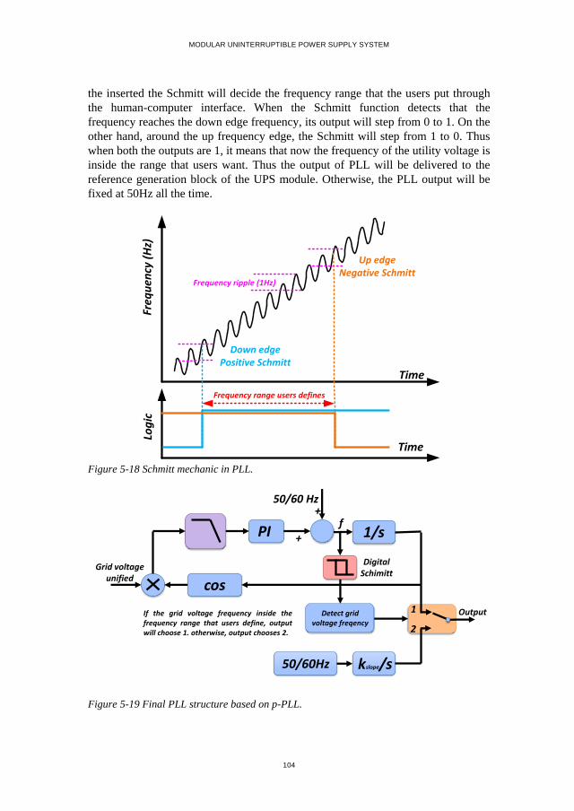
Aalborg Universitet Modular uninterruptible power supply system Zhang, Chi DOI (link to publication from Publisher): 10.5278/vbn.phd.engsci.00139 Publication date: 2016 Document Version Publisher's PDF, also known as Version of record Link to publication from Aalborg University Citation for published version (APA): Zhang, C. (2016). Modular uninterruptible power supply system. Aalborg Universitetsforlag. Ph.d.-serien for Det Teknisk-Naturvidenskabelige Fakultet, Aalborg Universitet https://doi.org/10.5278/vbn.phd.engsci.00139 General rights Copyright and moral rights for the publications made accessible in the public portal are retained by the authors and/or other copyright owners and it is a condition of accessing publications that users recognise and abide by the legal requirements associated with these rights. - Users may download and print one copy of any publication from the public portal for the purpose of private study or research. - You may not further distribute the material or use it for any profit-making activity or commercial gain - You may freely distribute the URL identifying the publication in the public portal - Take down policy If you believe that this document breaches copyright please contact us at [email protected] providing details, and we will remove access to the work immediately and investigate your claim. Downloaded from vbn.aau.dk on: February 20, 2022
Transcript
Aalborg Universitet
Modular uninterruptible power supply system
Zhang, Chi
DOI (link to publication from Publisher):10.5278/vbn.phd.engsci.00139
Publication date:2016
Document VersionPublisher's PDF, also known as Version of record
Link to publication from Aalborg University
Citation for published version (APA):Zhang, C. (2016). Modular uninterruptible power supply system. Aalborg Universitetsforlag. Ph.d.-serien for DetTeknisk-Naturvidenskabelige Fakultet, Aalborg Universitet https://doi.org/10.5278/vbn.phd.engsci.00139
General rightsCopyright and moral rights for the publications made accessible in the public portal are retained by the authors and/or other copyright ownersand it is a condition of accessing publications that users recognise and abide by the legal requirements associated with these rights.
- Users may download and print one copy of any publication from the public portal for the purpose of private study or research. - You may not further distribute the material or use it for any profit-making activity or commercial gain - You may freely distribute the URL identifying the publication in the public portal -
Take down policyIf you believe that this document breaches copyright please contact us at [email protected] providing details, and we will remove access tothe work immediately and investigate your claim.
Figure 1-1 UPS products evaluation criteria. ......................................................................... 18 Figure 1-2 UPS product performance score of different vendors. .......................................... 19 Figure 1-3 Global UPS market and typical applications. ....................................................... 20 Figure 1-4 Offline UPS system. ............................................................................................... 21 Figure 1-5 Line interactive UPS system. ................................................................................. 21 Figure 1-6 Line interactive UPS system. ................................................................................. 22 Figure 1-7 Half transformer-less online UPS system. ............................................................. 23 Figure 1-8 Total transformer-less online UPS system. ........................................................... 24 Figure 1-9 High frequency transformer online UPS system. ................................................... 24 Figure 1-10 Power electronic topologies for DC/AC. (a) 3P-HB (b) 3L-NPC (c) 3P-FB. ...... 25 Figure 1-11 Power electronic topologies for AC/DC. (a) Vienna rectifier. (b) 3L-4P-HB. .... 26 Figure 1-12 AC/DC stage integrated with battery charger. .................................................... 26 Figure 1-13 Transient duration requirements for online UPS system. (a) Limit for mode
change. (b) Limit for linear load change. (c) Limit for nonlinear load change. ...................... 27 Figure 2-1 Two promising modular UPS structures. (a) Partial modularized. (b) Total
modularized. ............................................................................................................................ 31 Figure 2-2 Simplified model for DC/AC parallel modules. ..................................................... 33 Figure 2-3 (a) Inductive condition. (b) resistive condition. ..................................................... 33 Figure 2-4 Virtual impedance and “Q–ϕ” control diagram. .................................................. 35 Figure 2-5 Active and reactive power sharing transient process. (a) only virtual impedance
(kph=0). (b) only Q–ϕ loops (Rvir=0). (c) using both virtual impedance and Q–ϕ loops. ..... 36 Figure 2-6 Proposed overall control diagram for the paralleled UPS system. ....................... 38 Figure 2-7 Phase synchronization performance. (a) Voltage amplitude recovery. (b) Phase
synchronization. ...................................................................................................................... 39 Figure 2-8 AC critical bus voltage when one module plugs out of the system. ....................... 40 Figure 2-9 Control diagram for online UPS system for plug’n’play capability –Simple Type.
................................................................................................................................................ 40 Figure 2-10 AC critical bus voltage when one module plugs out of the system. ..................... 42 Figure 2-11 Proposed Modular Online UPS Structure with active power filter. .................... 42 Figure 2-12 Overall control diagram for the UPS part. ......................................................... 42 Figure 2-13 Control scheme for the active power filter. ......................................................... 43 Figure 2-14 Performance under non-ideal utility. (a) Normal to Bypass. (b) Bypass to
Normal. (c) active power sharing. ........................................................................................... 44 Figure 2-15 FFT Analysis in different modes. (a) details at t6. (b)details at t8. (c) details at t10.
................................................................................................................................................ 44 Figure 2-16 DC/AC modules parallel performance. (a) Active power sharing between three
modules. (b) Reactive power sharing between three modules. ................................................ 45 Figure 2-17 Active and reactive power of 3 DC/AC modules. (a) Three DC/AC active power.
(b) Three DC/AC reactive power. ........................................................................................... 46
XIII
Figure 2-18 Active and reactive power sharing performance per phase. (a) Phase a active
and reactive power of three DC/AC. (b) Phase b active and reactive power of three DC/AC.
(c) Phase c active and reactive power of three DC/AC. .......................................................... 46 Figure 2-19 RMS voltage (Three DC/ACs and AC critical bus). (a) Phase a voltage RMS. (b)
Phase b voltage RMS. (c) Phase c voltage RMS. (d) AC critical bus voltage RMS. ................ 47 Figure 2-20 Phase synchronization tests. (a) Phase errors of 3 phases. (b) RMS voltage of AC
critical bus. .............................................................................................................................. 48 Figure 2-21 Synchronization process between vab_utility and vab_UPS. (a) Overall process. (b)
Details at tc. (c) Details at td. (d) Details at te. ......................................................................... 48 Figure 2-22 Voltage and current under unbalanced linear load condition. (a) Output voltage
and phase a current. (b) Output voltage and phase b current. (c) Output voltage and phase c
current. .................................................................................................................................... 49 Figure 2-23 Active and reactive power sharing performance under unbalanced nonlinear
load condition. (a) Active power. (b)-(d) Reactive power of phase a, b and c. ....................... 50 Figure 2-24 Voltage and current under unbalanced load condition. Output voltage and phase
a current when load is turned on and off (a)-(b) L+R type load. (c)-(d) L type load. ............. 51 Figure 2-25 UPS line to line voltage (phase a to b) and phase a current. (a) Balanced load
connected. (b) Balanced load disconnected. ........................................................................... 51 Figure 2-26 UPS line to line voltage (phase a to b) and phase a current. (a) Balanced load
connected. (b) Balanced load disconnected. ........................................................................... 52 Figure 2-27 Nonlinear load sharing performance. ................................................................. 52 Figure 2-28 AC critical bus voltage performance when one DC/AC stops. (a) Average type
under linear load. (b) Simple type under linear load. (c) Average type under nonlinear load.
(d) Simple type under nonlinear load. ..................................................................................... 52 Figure 2-29 Power performance when modules are plugging in and out. (a) active power
when module plugs out. (b) active power when module plugs in. (c) reactive power when
module plugs out. (d) reactive power when module plugs in. .................................................. 53 Figure 2-30 Real-time voltage performance of AC critical bus. (a) module plugs in. (b)
module plugs out. .................................................................................................................... 54 Figure 2-31 Synchronization performance. (a) overall process. (b) details at tj. (c) details at
tk. (c) details at tl. .................................................................................................................... 55 Figure 2-32 Active power filter performance. (a) load current. (b) DC/AC module #1 output
voltage with and without APF. (c) DC/AC module #2 output voltage with and without APF. 55 Figure 2-33 APF module performance. (a) DC capacitor voltage. (b) current reference in dq
frame. (c) output current in dq frame. ..................................................................................... 56 Figure 2-34 Power sharing performance among the DC/AC modules. (a) reactive power. (b)
active power. ........................................................................................................................... 56 Figure 2-35 AC critical bus voltage performance. (a) without APF. (b) with APF. ................ 57 Figure 2-36 Synchronization performance with the utility. (a) with APF enabled. (b) transient
performance while enabling and disabling the APF. .............................................................. 57 Figure 2-37 UPQC control modification in q axis. ................................................................. 57 Figure 2-38 UPQC voltage and current performance. ........................................................... 58 Figure 2-39 FFT performance of AC critical bus voltage. (a) before 0.02s. (b)after 0.02s. ... 59
MODULAR UNINTERRUPTIBLE POWER SUPPLY SYSTEM
XIV
Figure 2-40 Performance in case of communication failure. (a) Two modules in parallel. (b)
Three modules in parallel........................................................................................................ 60 Figure 3-1 Bode diagram of inner loop. (a) Bode diagram with variable kpv. (b) Bode diagram
with variable kpc. ..................................................................................................................... 62 Figure 3-2 Control loops simplification for voltage restoration and phase synchronization. . 62 Figure 3-3 pole-zero map for amplitude restoration. (a) PZ map with variable kpv_sec.
(b) PZ map with variable kiv_sec. ........................................................................................... 63 Figure 3-4 pole-zero map for phase restoration. (a) PZ map with variable kpθ_sec. (b) PZ
map with variable kiθ_sec. ...................................................................................................... 63 Figure 3-5 Pole-zero map for phase restoration. (a) Poles and zeros movement for phase
synchronize. (b) poles and zeros movement for amplitude recovery. ...................................... 64 Figure 3-6 Block diagram of the small-signal model for the proposed control. ...................... 65 Figure 3-7 Conventional PLL diagram. .................................................................................. 69 Figure 3-8 System performance while kpv_sec is 0.5, 2.5 and 5 (a) AC bus voltage. (b) Reactive
power. (c) Active power. ......................................................................................................... 77 Figure 3-9 System performance while kiv_sec is 5, 20.5 and 50. (a) AC bus voltage. (b) Reactive
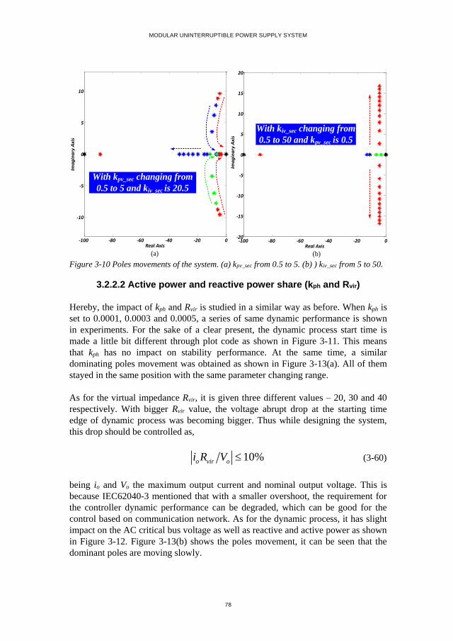
power. (c) Active power. ......................................................................................................... 77 Figure 3-10 Poles movements of the system. (a) kpv_sec from 0.5 to 5. (b) ) kiv_sec from 5 to 50.
................................................................................................................................................ 78 Figure 3-11 System performance while kph is 0.0001, 0.0003 and 0.0005. (a) AC bus voltage.
(b) Reactive power. (c) Active power. ..................................................................................... 79 Figure 3-12 System performance while Rvir is 20, 30 and 40. (a) AC bus voltage. (b) Reactive
power. (c) Active power. ......................................................................................................... 79 Figure 3-13 Poles movements of the system. (a) kph from 0.0001to 0.0005. (b) Rvir from 20 to
30. ........................................................................................................................................... 79 Figure 3-14 System performance while kpθ_sec is 0.2, 1 and 2. (a) AC bus voltage. (b) Reactive
power. (c) Active power. ......................................................................................................... 80 Figure 3-15 System performance while kiθ_sec is 10, 20 and 30. (a) AC bus voltage. (b)
Reactive power. (c) Active power. ........................................................................................... 80 Figure 3-16 Poles movements of the system. (a) kpθ_sec from 0.2 to 2. (b) ) kiθ_sec from 10 to 30.
................................................................................................................................................ 81 Figure 3-17 Synchronization process regarding different kpθ_sec and kiθ_sec. (a) kiθ_sec is 10, 20
and 30. (b) ) kpθ_sec is 0.2, 1.2 and 2.2. ..................................................................................... 81 Figure 4-1 Thermal model. (a) Power device model. (b) RC network of ZT/D(j-c). .................... 83 Figure 4-2 Path for zero sequence circulating current to flow. .............................................. 85 Figure 4-3 Cycle and backup rules. (a) N module cycling and n rests. (b) N-1 module cycling.
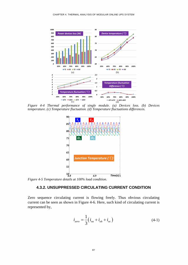
................................................................................................................................................ 85 Figure 4-4 Thermal performance of single module. (a) Devices loss. (b) Devices temperature.
(c) Temperature fluctuation. (d) Temperature fluctuations differences. .................................. 87 Figure 4-5 Temperature details at 100% load condition. ....................................................... 87 Figure 4-6 Zero sequence circulating current without suppressing. ....................................... 88 Figure 4-7 Thermal performance of three DC/AC modules. (a) module #1. (b) module #2. (c)
module #3. ............................................................................................................................... 88 Figure 4-8 Three DC/AC modules one leg devices temperature at 100% load condition. ...... 89
XV
Figure 4-9 Zero sequence circulating current without suppressing. ....................................... 89 Figure 4-10 Thermal performance with suppressing circulating current. Thermal
performance of three DC/AC modules. (a) module #1. (b) module #2. (c) module #3. ........... 90 Figure 4-11 Three modules one leg devices temperature at 100% load condition with
suppressing. ............................................................................................................................. 91 Figure 5-1 Control process for frequency regulation, phase jump and combined methods. ... 93 Figure 5-2 Frequency performance. (a) pPLL. (b) SOGI-PLL. .............................................. 94 Figure 5-3 Frequency performance with variable kQ. (a) pPLL. (b) SOGI-PLL. .................... 95 Figure 5-4 Resonant part diagram with saturation. ................................................................ 95 Figure 5-5 Voltage performance without anti-windup. (a DC voltage ramp. (b) DC voltage
step. ......................................................................................................................................... 96 Figure 5-6 Resonators with anti-windup capability. ............................................................... 96 Figure 5-7 Voltage performance with anti-windup. (a) DC voltage ramp. (b) DC voltage step.
................................................................................................................................................ 97 Figure 5-8 Direct anti-windup for resonators. ........................................................................ 97 Figure 5-9 Voltage performance with direct anti-windup. (a) DC voltage ramp. (b) DC
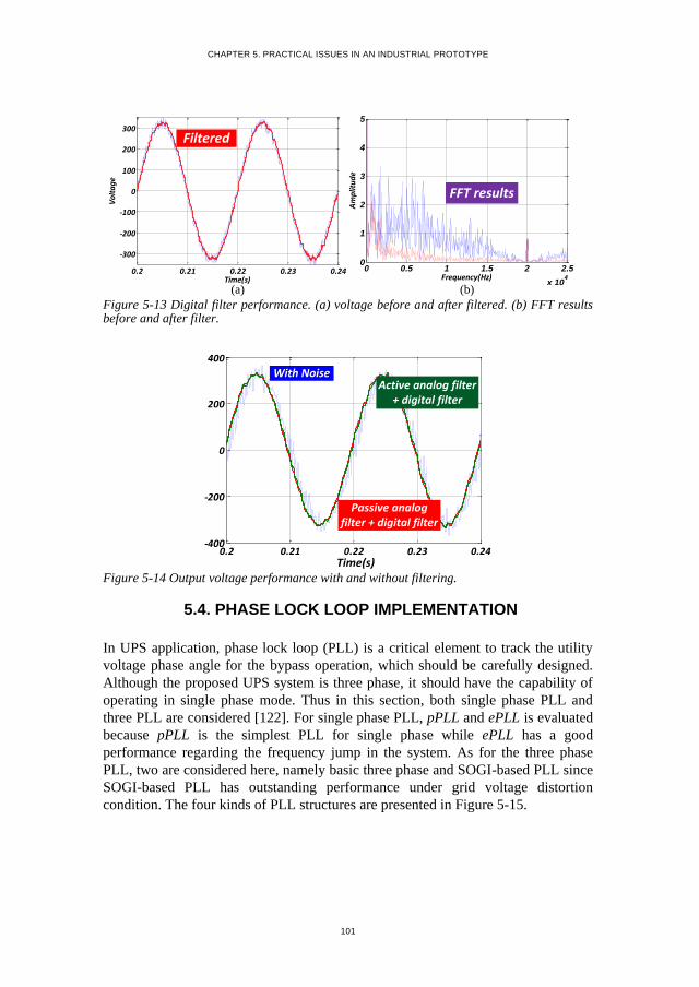
voltage step. ............................................................................................................................ 97 Figure 5-10 AD hardware for voltage measurement. (a) single polar. (b) bi-polar. ............... 98 Figure 5-11 Low pass filter for AD noise. (a) passive type. (b) active type (Sallen-Key). ....... 99 Figure 5-12 Performance of both passive and active analog filter. ...................................... 100 Figure 5-13 Digital filter performance. (a) voltage before and after filtered. (b) FFT results
before and after filter. ........................................................................................................... 101 Figure 5-14 Output voltage performance with and without filtering. .................................... 101 Figure 5-15 Different PLL structure. (a) pPLL. (b) ePLL. (c) basic three phase PLL. (d)
SOGI-based PLL. .................................................................................................................. 102 Figure 5-16 Different PLL dynamic performance in case of frequency jump. (a) pPLL. (b)
ePLL. (c) basic three phase PLL. (d) SOGI-based PLL. ....................................................... 103 Figure 5-17 Schmitt function. ................................................................................................ 103 Figure 5-18 Schmitt mechanic in PLL. .................................................................................. 104 Figure 5-19 Final PLL structure based on p-PLL. ................................................................ 104 Figure 5-20 Transient mechanics between output 1 and 2 of PLL. ....................................... 105 Figure 5-21 Proposed PLL performance. (a) performance from unsynchronized to
synchronized condition. (b) performance of exiting synchronized. ....................................... 106 Figure 5-22 Final prototype of UPS module. (a) UPS module in Leaneco. (b) UPS module in
Salicru. .................................................................................................................................. 107 Figure 5-23 Power supply for the ADC part of DSP. ............................................................ 108 Figure 5-24 Output voltage performance. (a) output voltage in case of self-excited. (b) output
voltage after improved. ......................................................................................................... 108 Figure 5-25 Test performance. (a) full load. (b) soft-start process. ...................................... 109 Figure 5-26 Soft-start details. (a) details at tt1. (b) details at tt2. (c) details at tt3. (d) details at
Table 2-1. THD Analysis results ............................................................................................. 45 Table 2-2. AC critical bus voltage and UPS output current THD. .......................................... 59 Table 4-1. DC/AC electrical information ................................................................................ 84 Table 4-2. IGBT pack thermal information ............................................................................. 84
17
PART I THESIS REPORT MAIN CONTENT
Part I is the main content for the Ph. D thesis. It is a collection of the published
paper. It gives a detailed presentation, explanation of the Ph. D project.
The main content of the thesis report is based on the papers that the author had
published in the international journals, conferences and the work in the company.
The relationship between thesis report and published papers, collaborative work in a
Spanish UPS company, Salicru S/A is shown in the following table. And the in the
main content, the relationship is marked detailed in each chapter.
Chapters Relevant publications
1
2 A1, A3, A4, A5, A6, A8
3 A2, A3
4 A7
5 collaborative work in a Spanish
UPS company, Salicru S/A
6
MODULAR UNINTERRUPTIBLE POWER SUPPLY SYSTEM
18
CHAPTER 1. INTRODUCTION
This chapter gives the background, motivation and organization of my Ph. D work.
The state-of-art of uninterruptible power supply (UPS) system is illustrated as well
as the existing products of modern modular UPS system. Finally, the structure of
the thesis is presented given in details.
1.1. STATE OF ART OF UNINTERRUPTIBLE POWER SUPPLY SYSTEMS
The booming development of the modern electronic devices, such as data center,
mobile base station, among others, is emerging in human being’s everyday life [1].
Normally such kind of loads either is distributed widely across a big area or
requires continuous reliable energy supply. As a consequence, UPS system is
receiving more and more attention from both vendors and consumers. On the other
hand, continuing demand from the downstream refining and petrochemicals,
upstream oil & gas, mining industries and investments in automation to raise
productivity, flexibility, and address regulatory and safety needs will also drive the
demand for the industrial UPS equipment [2]. For the evaluation of UPS products,
vendor and product side evaluation share the same importance as shown in Figure
1-1 [3].
Figure 1-1 UPS products evaluation criteria.
features usability affordability architecture vendor product
35%
25%
20%
20%
50%50%
viability channel strategy reach
20%
20%30%
30%
· Features: the solution provides basic and advanced feature/functionality
· Affordability: the five years TCO of solution is economical
· Usability: the solution can be easily integrated with facilities management systems and generators
· Architecture: the solution can be easily scaled for future growth and allows for hot-swapping
· Viability: vendor is profitable, knowledge, and will be around for the long-term
· Strategy: vendor is committed to the space and has future product and portfolio roadmap
· Reach: vendor offers global coverage and is able to sell and provide post-sales support
· Channel: vendor channel strategy is appropriate and the channels themselves are strong
Pro
du
ct s
ide
Ven
do
r side
CHAPTER 1. INTRODUCTION
19
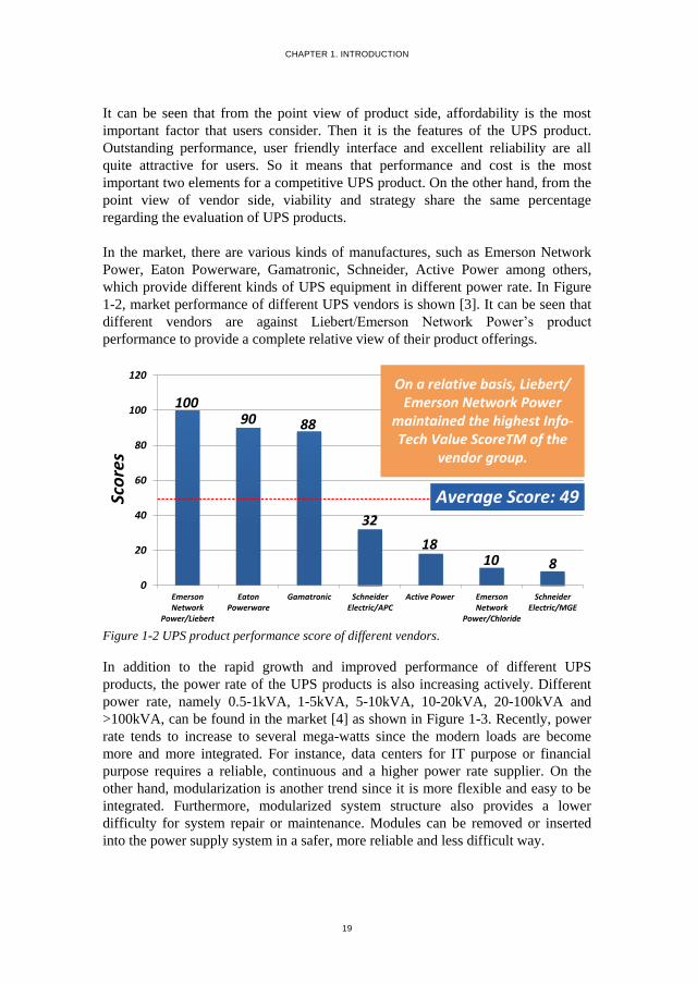
It can be seen that from the point view of product side, affordability is the most
important factor that users consider. Then it is the features of the UPS product.
Outstanding performance, user friendly interface and excellent reliability are all
quite attractive for users. So it means that performance and cost is the most
important two elements for a competitive UPS product. On the other hand, from the
point view of vendor side, viability and strategy share the same percentage
regarding the evaluation of UPS products.
In the market, there are various kinds of manufactures, such as Emerson Network
Power, Eaton Powerware, Gamatronic, Schneider, Active Power among others,
which provide different kinds of UPS equipment in different power rate. In Figure
1-2, market performance of different UPS vendors is shown [3]. It can be seen that
different vendors are against Liebert/Emerson Network Power’s product
performance to provide a complete relative view of their product offerings.
Figure 1-2 UPS product performance score of different vendors.
In addition to the rapid growth and improved performance of different UPS
products, the power rate of the UPS products is also increasing actively. Different
power rate, namely 0.5-1kVA, 1-5kVA, 5-10kVA, 10-20kVA, 20-100kVA and
>100kVA, can be found in the market [4] as shown in Figure 1-3. Recently, power
rate tends to increase to several mega-watts since the modern loads are become
more and more integrated. For instance, data centers for IT purpose or financial
purpose requires a reliable, continuous and a higher power rate supplier. On the
other hand, modularization is another trend since it is more flexible and easy to be
integrated. Furthermore, modularized system structure also provides a lower
difficulty for system repair or maintenance. Modules can be removed or inserted
into the power supply system in a safer, more reliable and less difficult way.
0
20
40
60
80
100
120
EmersonNetwork
Power/Liebert
EatonPowerware
Gamatronic SchneiderElectric/APC
Active Power EmersonNetwork
Power/Chloride
SchneiderElectric/MGE
Sco
res
Average Score: 49
10090 88
32
1810 8
On a relative basis, Liebert/Emerson Network Power
maintained the highest Info-Tech Value ScoreTM of the
vendor group.
MODULAR UNINTERRUPTIBLE POWER SUPPLY SYSTEM
20
Figure 1-3 Global UPS market and typical applications.
1.2. UPS SYSTEM ARCHITECTURES
1.2.1. THREE TYPES OF CONVENTIONAL UPS SYSTEM ARCHITECTURES
On the basis of the International Electrotechnical Commission Standard 62040-3,
three basic categories can be found, namely offline UPS [5], [6], line interactive
UPS [7]-[10] and online UPS [11], [12] based on the energy flow direction in
different operating conditions. In the following sub-sections, each kind of UPS
system architectures will be analyzed.
1.2.1.1 Offline UPS system
Figure 1-4 shows a conventional offline type UPS. Normally, offline UPS module
is rated below 2kVA [5]. It is composed of AC/DC, DC/AC, battery pack and static
bypass switch (SCR). If the utility is in good condition, energy will flow through
the SCR and support the load directly. Nevertheless, SCR will be open and battery
pack will be started and transfer energy to load. When battery pack uses up its
energy, AC/DC will start to charge the battery and support the load at the same
time. It can be seen that offline UPS doesn’t provide any isolation between the
utility and the loads. As a result, any utility distortion will affect the load directly.
This puts a higher requirement on the protection of loads. In some specific
application scenarios, passive filter is used to reduce this kind of impact, such as
voltage spikes, sags or oscillations [11].
<1kVA14%
1-10kVA36%10-100kVA
24%
100-250kVA10%
>250kVA16%
· PCs· Home appliance· POS equipment· Retail
· In-rack server· ATMs
· Medical equipment
· Industrial PLCs
· Network switches
· Labs· Small security system
· Small data centers
· Computer room
· Large medical equipment
· Large security system
· Mid-sized and large data center
· Central backbone of larger data centers
CHAPTER 1. INTRODUCTION
21
Figure 1-4 Offline UPS system.
Figure 1-5 Line interactive UPS system.
1.2.1.2 Line interactive UPS system
Figure 1-5 presents a typical line-interactive UPS system. Normally, it operates in
medium power rate application. The operating rule is a little bit different than the
offline UPS system. The AC/DC, DC/AC and battery pack works together not only
as a power supporter but also as a compensation loop. For instance, the AC/DC can
suppress the utility voltage distortion through the series transformer [7], [8]. On the
other hand, the PFC function can be also achieved [9]. Since the loads are supported
by the two energy paths at the same time, thus DC/AC only provide around 10%-
20% of the total load power, which means a higher efficiency [10]. However, the
control structures for AC/DC and DC/AC are different and complex. Operating
modes transient process will happen during the UPS operation. On the other hand,
the line series transformer will increase the cost and volume of the UPS system.
Nowadays, it is difficult for vendors to accept a higher cost and lower reliability. At
the same time, the DC/AC can inject active power into the load to regulate the
power factor. Such kind of the equipment is called unified power quality
compensator (UPQC).
AC/DC DC/AC
Battery Pack
Utility
Static Bypass Switch
Load
Normal
Backup
AC/DC DC/AC
Battery Pack
Utility
Static Bypass Switch
Load
Normal
Backup
Interactive
Series Transformer
MODULAR UNINTERRUPTIBLE POWER SUPPLY SYSTEM
22
1.2.1.3 Online UPS system
Online UPS system, also known as inverter preferred UPS or double conversion
UPS, is more popular due to its outstanding regulation ability on power quality
[11]. It is designed for higher power rate application scenarios. Its good decoupling
ability of the utility and the load under power outage is another reason that makes it
attractive for consumers [12].
As shown in Figure 1-6, a typical online UPS module is composed of a double
conversion stage structure and a static bypass switch. However, the static bypass
switch is not the main role of transferring power. The AC/DC, battery and DC/AC
will take the role of regulating power. Only in some emergency conditions, the
static bypass switch will be activated.
In Figure 1-6, a conventional online UPS system is shown. Under utility normal
condition, the utility power is regulated through the two stage converter and
injected into the load while AC/DC also acts the charger for the battery pack. Once
the utility errors occur, system enters backup mode and battery pack starts to
regulate system output power. Furthermore, static bypass will be turned on in event
of power conditioner failure [11]. By removing the series transformer, online UPS
system is cost-effective and weight-effective.
Figure 1-6 Line interactive UPS system.
It can be seen that this structure is more direct on power regulating without any
galvanic isolation or transformers. AC/DC is responsible for the harmonic
controlling of the utility side while DC/AC modules are regulating the output
voltage quality of the system. Normally, the required load power will regulate a two
stage system and then transferred to the load. Although it may have a larger amount
of losses, its outstanding power regulating capability makes it more attractive.
Similarly, it has a lower controllability on the battery power management.
AC/DC DC/AC
Battery Pack
Utility
Static Bypass Switch
Load
Normal
Backup
CHAPTER 1. INTRODUCTION
23
1.2.2. EVOLUTION OF ONLINE UPS SYSTEM ARCHITECTURE
Since the online UPS system is aimed at high power and voltage application
scenarios, a series of improved online UPS structure have been proposed in [13]-
[22], which are better at regulating active power consumption to achieve unity
power factor. Additional DC/DC [13]-[17] and high frequency transformer [18]-
[21] are the two main issues that are chosen to achieve a cost-effective, volume-
effective and more reliable online UPS system.
1.2.2.1 Half transformer-less online UPS system
In half transformer-less online UPS as shown in Figure 1-7, one additional DC/DC
is inserted into the system to improve power quality [13], [14] and the
controllability on battery pack in the system. On the other hand, a lower DC bus
voltage is achieved, which indicates fewer battery packs in series and higher safety.
However, input or output line frequency transformer still decrease system’s
efficiency and lead to more current stress on converters [15]. On the other hand, the
system becomes three stages at least, which means a lower overall efficiency of the
whole system. The cascaded converter structure also requires more efforts on the
converter design. Converter type load impedance feature is a constant power type,
which is a negative resistive type. From the point of control side, such kind of load
2.3.1. BASIC PARALLEL CONTROL [PUBLICATION A3, A5]
Conventional hybrid based methods are designed based on the fact that the line
impedance is designed to be mainly inductive. Thus active power can be regulated
by the system frequency and reactive power is controlled by the output voltage
amplitude as shown in Figure 2-3(a). However, with such kind of method, the UPS
system frequency is fluctuated, which is an undesired condition for an online UPS
system because the changeable frequency will have negative impact the online UPS
system bypass process. On the other hand, both active power and reactive power are
required to be calculated in order to achieve the control. This means that a complex
control architecture is mandatory for the system. In order to simply the control,
virtual impedance [75]-[80] concept is introduced to replace the real inductive line
impedance. Thus DC/AC module output impedance can be designed manually to be
mainly inductive.
As a consequence, similar idea is used. Through changing the virtual impedance to
be resistive, thus output impedance of DC/AC module can be forced to be designed
as resistive. In this condition, the DC/AC module output power can be controlled in
a different way, as shown in Figure 2-3(b), ie active power is related to the
amplitude while the reactive power is concerned by the phase angle for frequency.
Considering the fact that a variation in the system frequency is not desired for the
bypass process for the online UPS system, phase signal is chosen to regulate the
DC/AC module output reactive power. Since the phase angle is obtained from the
phase lock loop (PLL), the phase angel is tightly related with the frequency. Thus
during the time that control starts to modify the phase angle, the system frequency
will be jumped suddenly and move back to nominal value afterwards, which is
called “Q–ϕ” control.
Based on Figure 2-2, DC/AC module output power can be derived as
2
_ _
_cos( )nk bus k bus k
nk nk bus k
vir vir
V V VP
R R (2-1)
_
_sin( )nk bus k
nk nk bus k
vir
V VQ
R (2-2)
being Pnk and Qnk the active and reactive power injected by the module n in phase k,
Vnk voltage value of the module n in phase k, δnk module n phase k angle
information, Vbus_k the critical bus phase k voltage, and δbus_k the critical bus phase k
CHAPTER 2. CONTROL STRATEGIES FOR MODULAR ONLINE UPS SYSTEM
35
phase information. In real application scenarios, the phase angle difference (δnk-
δbus_k) between DC/AC module and AC critical bus is quite small. So it can be
treated as zero. Thus the two equations are rewritten as following,
Figure 2-4 Virtual impedance and “Q–ϕ” control diagram.
_
_
bus k
nk nk bus k
vir
VP V V
R (2-3)
_
_( )nk bus k
nk nk bus k
vir
V VQ
R (2-4)
From the equations above, it can be concluded that the output active power of the
DC/AC module can be estimated by the output voltage amplitude while phase angle
can be used to regulate the output reactive power of DC/AC modules. By using the
virtual impedance (resistive), inductor current will be used to regulate the voltage
amplitude. Consequently, the output active power can be controlled. The proposed
control architecture is shown in Figure 2-4,
sinnk nkref g n vir nLabcV V t R i (2-5)
n nkref p nh kQk (2-6)
Here n is DC/AC module sequence number, k is the phase order, Vnkref is phase k
reference voltage, Rvir is virtual resistor value, δg is the grid phase information, δnkref
is module n phase k phase reference, kph is Q–ϕ coefficients, and Qnk is module n
phase k reactive power. The inner loop for each DC/AC module use the
iLabc
vCabc
δn
vnk
δnkref+
+
MODULAR UNINTERRUPTIBLE POWER SUPPLY SYSTEM
36
conventional double loop structure (voltage and current loop), which uses two
typical PR controllers due to its capability of suppressing harmonics [81]-[85],
2 2 2 2
5,7
( )( )
rv hrvv pv
ho o
k s k sG s k
s s h
(2-7)
2 2 2 2
5,7
( )( )
rc hrcc pc
ho o
k s k sG s k
s s h
(2-8)
being kpv, krv the basic voltage loop PR controller parameter, ωo the 2*π*50 rad/s,
khrv the compensation term for hth harmonic, h the harmonic number, kpc, krc the
basic current loop PR controller parameter, and khrc the hth harmonic current
compensation value.
Figure 2-5 Active and reactive power sharing transient process. (a) only virtual impedance (kph=0). (b) only Q–ϕ loops (Rvir=0). (c) using both virtual impedance and Q–ϕ loops.
t3
Phase a voltage of DC/AC module #1
t1 Phase a voltage of DC/AC module #2
Phase a angle of DC/AC module #1
Phase a angle of DC/AC module #2
Active Power of DC/AC module #2
Active Power of DC/AC module #1
Reactive Power of DC/AC module #2
Reactive Power of DC/AC module #1
t2
(a) (b)
(c)
Phase a voltage of DC/AC module #1
Phase a voltage of DC/AC module #2
Phase a angle of DC/AC module #1
Phase a angle of DC/AC module #2
Active Power of DC/AC module #2
Active Power of DC/AC module #1
Reactive Power of DC/AC module #2
Reactive Power of DC/AC module #1
Phase a voltage of DC/AC module #1
Phase a voltage of DC/AC module #2
Phase a angle of DC/AC module #1
Phase a angle of DC/AC module #2
Active Power of DC/AC module #2
Active Power of DC/AC module #1
Reactive Power of DC/AC module #2
Reactive Power of DC/AC module #1
CHAPTER 2. CONTROL STRATEGIES FOR MODULAR ONLINE UPS SYSTEM
37
With the help of the simulation software PLECS, a basic parallel system composed
of two DC/AC modules was established to verify the proposed control mechanism.
The results are presented in Figure 2-5. In Figure 2-5, the result was obtained by
disabling reactive power regulation, ie kph is set to 0. Although the virtual
impedance part intends to make two DC/AC modules output active power be
convergent to the same value, there are still some static errors due to the initial
given phase angle difference. DC/AC module #1 gives higher output active power
that DC/AC module #2 and this means that DC/AC module #2 output voltage
amplitude is larger than #1 based on (2-5). Then (2-6) is enabled, two modules
output voltage amplitude is controlled further until they reach the same value by
modifying phase angle, ie DC/AC module reactive power. On the other hand, the
phase angle difference between two DC/AC modules is moved to the same value,
which contributes to reactive power equally sharing as shown in Figure 2-5(c).
Moreover, virtual impedance part is disabled and the Q–ϕ takes the roles of parallel
two DC/AC modules. The test result is shown in Figure 2-5(b). The phase angle
difference is eliminated to zero, which force two modules output reactive power
move to the same value. Nevertheless, due to the output voltage amplitude
deviations, the reactive power is not well shared. By applying (2-5), the voltage
amplitude is regulated to the same value. And both active power and reactive power
are well shared between two DC/AC modules as shown in Figure 2-5(c).
2.3.2. VOLTAGE AMPLITUDE RECOVERING AND PHASE ANGLE SYNCHRONIZATION [PUBLICATION A1-6]
Due to the existence of virtual resistor, AC critical bus voltage amplitude, which is
made up of several DC/AC modules output voltage, will have voltage drop
compared with reference value. Moreover, reactive power regulation will generate a
phase shift on the AC critical bus voltage. Thus voltage amplitude recovery and
phase angle reduction and synchronization should be taken into account. There are
two kinds of control strategies considered here – Average Type and Simple Type.
2.3.2.1 Average Type [Publication A3, A5]
Average type utilizes the average information of voltage, phase of different DC/AC
modules as the feedback information for recovery. Through the CAN bus network,
each DC/AC module will broadcast its own voltage amplitude information and
phase angle value to the recovery control part.
For the voltage amplitude recovery, when all DC/AC modules output voltage
amplitude is received, the averaged value will be calculated,
MODULAR UNINTERRUPTIBLE POWER SUPPLY SYSTEM
38
Figure 2-6 Proposed overall control diagram for the paralleled UPS system.
_
1
1 n
a avr ia
i
V Vn
(2-9)
Here Via is phase a RMS voltage amplitude of module #i. Compared with the
reference, a compensated value for the voltage amplitude reference is generated by
using a PI controller each phase respectively as shown in Figure 2-6,
_ _ _ _
_ sec
_ _ _ sec
( )
k rec kref r k avr v rec
iv
kref r k avr pv
v V V G s
kV V k
s
(2-10)
being vk_rec, Vkref_r, Vk_avr, kpv_sec and kiv_sec as restoration value of voltage amplitude,
RMS voltage reference of phase k in central controller, average value of phase k
RMS voltage value, voltage proportional control parameter and voltage integral
control parameter respectively. And this value will be broadcast through CAN bus
network to each module.
On the other hand, the phase angle regulation and synchronization will be carried
out in a similar way. Hereby the phase angle is required to be tightly synchronized
with the utility voltage in case of bypass operation under emergency condition.
Thus the phase synchronization reference is the utility voltage angle. This control is
vk_ref
…
v1a
δ1
v2δ2
v3 δ3
AC critical
bus
CAN Bus
δk_ref
v2a v3av1
δ1aδ2a δ3a
+
+
CHAPTER 2. CONTROL STRATEGIES FOR MODULAR ONLINE UPS SYSTEM
39
also executed in three phase respectively. Take phase a for instance, the averaged
phase angle is derived,
_
1
1( )
n
a avr ia
in
(2-11)
where δia is the phase a angle of module #i. By comparing it with the utility phase
angle, the compensated value for each phase angle reference is calculated through a
typical PI controller and sent through the CAN bus network as shown in Figure 2-6,
_ _ _ _
_ _ _ _
( )
=
k rec kref r k avr ph rec
kref r k avr p rec i rec
G s
k k s
(2-12)
being δk_rec, δkref_r, δk_avr kpθ_rec and kiθ_sec as phase restoration value of phase k, phase
reference in central controller (utility phase angle), average value of phase k angle,
phase synchronization proportional control parameter and phase synchronization
integral control parameter respectively.
Simulation results are presented in Figure 2-7, which is obtained from PLECS.
Figure 2-7(a) shows the performance of voltage amplitude recovery. A load step is
given at 0.6s, there will be a voltage sag based on (2-5) as shown in Figure 2-7(a).
Due to the voltage recovery control, the RMS value of the UPS output voltage
amplitude and RMS value is increased gradually to the nominal value – 230V.
Moreover, the phase regulation and synchronization performance is shown in
Figure 2-7(b). Through enabling the phase control part, the phase error between
grid voltage and UPS AC critical bus voltage will be decreased until it will reach
Normal 0.7874 0.7862 0.8151 1.4674 1.4788 1.4179 49.7656 51.8558 48.1405
2.4. EXPERIMENTAL RESULTS AND VALIDATION [PUBLICATION A1-6]
In the standard IEC 62040-3, there are requirements that relates to online UPS
system both steady and dynamic performance. In this section, experiments were
carried out in the Microgrid Research Laboratories to validate the proposed control
methods feasibility.
2.4.1. POWER SHARING AND VOLTAGE TRANSIENT PERFORMANCE [PUBLICATION A3, A5]
At time ta (around 4s), DC/AC module #3 is ordered to be plug into the system,
which is connected to a hybrid load (uncontrolled rectifier and resistive load). It can
be seen that the active power is gradually shared among the three modules in Figure
2-16(a). A similar process is taking place for the reactive power in Figure 2-16(b).
Figure 2-16 DC/AC modules parallel performance. (a) Active power sharing between three modules. (b) Reactive power sharing between three modules.
(a) (b)
Rea
ctiv
e P
ow
er (
Va
r)
Act
ive
Po
wer
(W
)
P1P2
P3
Q3
Q2
Q1
ta tb
MODULAR UNINTERRUPTIBLE POWER SUPPLY SYSTEM
46
Figure 2-17 Active and reactive power of 3 DC/AC modules. (a) Three DC/AC active power. (b) Three DC/AC reactive power.
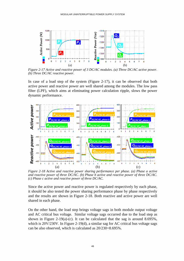
In case of a load step of the system (Figure 2-17), it can be observed that both
active power and reactive power are well shared among the modules. The low pass
filter (LPF), which aims at eliminating power calculation ripple, slows the power
dynamic performance.
Figure 2-18 Active and reactive power sharing performance per phase. (a) Phase a active and reactive power of three DC/AC. (b) Phase b active and reactive power of three DC/AC. (c) Phase c active and reactive power of three DC/AC.
Since the active power and reactive power is regulated respectively by each phase,
it should be also tested the power sharing performance phase by phase respectively
and the results are shown in Figure 2-18. Both reactive and active power are well
shared in each phase.
On the other hand, the load step brings voltage sags in both module output voltage
and AC critical bus voltage. Similar voltage sags occurred due to the load step as
shown in Figure 2-19(a)-(c). It can be calculated that the sag is around 8.695%,
which is 20V/230V. In Figure 2-19(d), a similar sag for AC critical bus voltage sags
can be also observed, which is calculated as 20/230=8.695%.
P3 P2
P1
Q1
Q2
Q3
(a) (b)
Act
ive
Pow
er (
W)
Rea
ctiv
e P
ow
er (
Var)
(a) (b) (c)
PDC/AC #1_phase a
PDC/AC #2_phase a
PDC/AC #3_phase a
QDC/AC #1_phase a
QDC/AC #2_phase a
QDC/AC #3_phase a
Act
ive
po
wer
Rea
ctiv
e p
ow
er
PDC/AC #1_phase b
PDC/AC #2_phase b
PDC/AC #3_phase b
PDC/AC #1_phase c
PDC/AC #2_phase c
PDC/AC #3_phase c
QDC/AC #1_phase b
QDC/AC #2_phase b
QDC/AC #3_phase b
QDC/AC #1_phase c
QDC/AC #2_phase c
QDC/AC #3_phase c
CHAPTER 2. CONTROL STRATEGIES FOR MODULAR ONLINE UPS SYSTEM
47
Figure 2-19 RMS voltage (Three DC/ACs and AC critical bus). (a) Phase a voltage RMS. (b) Phase b voltage RMS. (c) Phase c voltage RMS. (d) AC critical bus voltage RMS.
Another capability of the system is the phase synchronization with the phase
reference, which may be the utility phase angle of each phase or an external source
phase angle information, such as diesel generator or other kinds of generator. At
around 0.5s, the phase synchronization function is enabled and phase errors
between module output voltage and main grid is reduced gradually, as shown in
Figure 2-20(a). And the errors are controlled around zero finally. However, when
the phase synchronization function is enabled, this will bring a voltage spike on the
modules output voltage, which is shown in Figure 2-20(b). Since the amplitude
recovery function is also active, the output voltage amplitude is tightly regulated.
After a few cycles, the output voltage moves back to 230V (RMS). In Figure 2-
20(b), the spike is 7.5V/230V (3.26%), which is under 10% of the nominal output
voltage amplitude.
For a typical online UPS system, it should have the capability of keeping itself
tightly synchronized with utility voltage all the time. This will allow the system to
transfer to bypass operation smoothly without bringing any voltage oscillation.
Figure 2-21 shows the synchronization performance for the proposed modular
online UPS system. Hereby, the line to line voltage (phase a to phase b) is
presented. With the phase error reducing gradually, UPS output voltage and the
utility voltage is moving towards together. And during the whole process, it can be
seen that the voltage is stable during the whole synchronization process. Once the
phase error reaches zero, the error is tightly controlled around zero and two voltages
are matched.
vca1_rms
vca2_rms
vca3_rms
vca_avr vcb_avr
vca_avr
(a) (b)
(c) (d)
vcb1_rms
vcb2_rmsvcb3_rms
vcc1_rms
vcc2_rmsvcc3_rms
Ph
ase
a v
olt
ag
e R
MS
of
3 m
od
ule
s
Ph
ase
b v
olt
ag
e R
MS
of
3 m
od
ule
s
Ph
ase
c v
olt
ag
e R
MS
of
3 m
od
ule
s
AC
cri
tica
l bu
s vo
lta
ge
RM
S
MODULAR UNINTERRUPTIBLE POWER SUPPLY SYSTEM
48
Figure 2-20 Phase synchronization tests. (a) Phase errors of 3 phases. (b) RMS voltage of AC critical bus.
Figure 2-21 Synchronization process between vab_utility and vab_UPS. (a) Overall process. (b) Details at tc. (c) Details at td. (d) Details at te.
2.4.3. LINEAR LOAD PERFORMANCE [PUBLICATION A3, A5]
Linear load condition is the basic load type for an online UPS system. Hereby
resistors are used to emulate linear load condition-balanced type and unbalanced
type.
First, unbalanced type is tested. Figure 2-22 shows the system performance when
one resistor is connected between phase a and phase b while phase c is left
unconnected. In this condition, the load is highly unbalanced and the system
requires more time to recover the amplitude to the nominal value. It can be seen that
(a)
Pha_error
Phb_error
Phc_error
(b)
vca1_rms
vcb1_rms
vcc1_rms
Ph
ase
err
ors
AC
bu
s vo
lta
ge
tc td teErrors between UPS
output voltage and utility
Vab of UPS and utility
Vbc
Vca
(a) (b)
(c) (d)
CHAPTER 2. CONTROL STRATEGIES FOR MODULAR ONLINE UPS SYSTEM
49
it needs around 5 cycles, ie 100ms. In the overall process, the voltage shape is kept
sinusoidal.
Moreover, more types of unbalanced load are tested in order to verify the control
feasibility. An L+R type load is put between phase a and phase b and phase c is
vacant. In the scenario, each phase had to deal with different amount of reactive
power, which means that its phase angle is regulated respectively. In Figure 2-23, it
can be observed that when the load step was performed at tf and tg, each phase
reactive power is well shared during the whole process as well as the active power
of each module.
Figure 2-22 Voltage and current under unbalanced linear load condition. (a) Output voltage and phase a current. (b) Output voltage and phase b current. (c) Output voltage and phase c current.
(a)
(b)
(c)
ia
vab vbc vca
ia
vab vbc vca
ib
vab vbc vca
ib
vab vbc vca
ic
vab vbc vca
ic
vab vbc vca
10A/div
250V/div
10A/div
250V/div
10A/div
250V/div
10A/div
250V/div
10A/div
250V/div
10A/div
250V/div
MODULAR UNINTERRUPTIBLE POWER SUPPLY SYSTEM
50
The AC critical bus voltage real-time performance at tf and tg is presented in Figure
2-24(a) and (b). A quite small voltage overshoot is observed. In case of the load
connection, the AC critical bus voltage amplitude needs around 30ms to recover to
its nominal value. When the load is disconnected, the transient time is smaller,
which is around 20ms. In order to test the performance further, a pure L type load is
replaced. In Figure 2-24(c) and (d), the results are presented and it can be concluded
that the voltage transient is smooth and faster.
Finally, the simplest type of linear load is balanced type. Three phases are all
connected with the same resistor. The performance is shown in Figure 2-25. It can
be seen that when the balanced resistive load is connected and disconnected, the
voltage transient time is around 40ms.
Figure 2-23 Active and reactive power sharing performance under unbalanced nonlinear load condition. (a) Active power. (b)-(d) Reactive power of phase a, b and c.
Rea
ctiv
e P
ow
er (
Va
r)
Act
ive
Po
wer
(W
)R
eact
ive
Po
wer
(V
ar)
Rea
ctiv
e P
ow
er (
Va
r)
P1
P2
P3
Q1_a
Q2_a
Q3_a
Q1_b
Q2_b
Q3_b
Q1_c
Q2_c
Q3_c
(a) (b)
(c) (d)
tf tg tf tg
tf tg tf tg
CHAPTER 2. CONTROL STRATEGIES FOR MODULAR ONLINE UPS SYSTEM
51
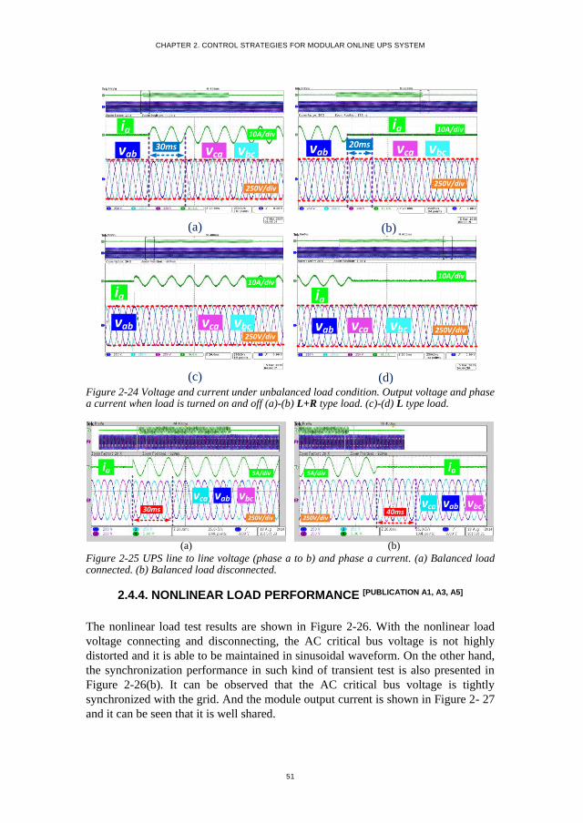
Figure 2-24 Voltage and current under unbalanced load condition. Output voltage and phase a current when load is turned on and off (a)-(b) L+R type load. (c)-(d) L type load.
Figure 2-25 UPS line to line voltage (phase a to b) and phase a current. (a) Balanced load connected. (b) Balanced load disconnected.
The nonlinear load test results are shown in Figure 2-26. With the nonlinear load
voltage connecting and disconnecting, the AC critical bus voltage is not highly
distorted and it is able to be maintained in sinusoidal waveform. On the other hand,
the synchronization performance in such kind of transient test is also presented in
Figure 2-26(b). It can be observed that the AC critical bus voltage is tightly
synchronized with the grid. And the module output current is shown in Figure 2- 27
and it can be seen that it is well shared.
ia
vab vbcvca
(a) (b)
(c) (d)
30ms 20ms
ia
vab vbcvca
ia
vab vbcvca
ia
vab vbcvca
10A/div
250V/div
10A/div
250V/div
10A/div
250V/div
10A/div
250V/div
(a)
vab vbcvca
ia
(b)
30msvab vbcvca
ia
40ms
5A/div
250V/div
5A/div
250V/div
MODULAR UNINTERRUPTIBLE POWER SUPPLY SYSTEM
52
Figure 2-26 UPS line to line voltage (phase a to b) and phase a current. (a) Balanced load connected. (b) Balanced load disconnected.
Figure 2-27 Nonlinear load sharing performance.
Figure 2-28 AC critical bus voltage performance when one DC/AC stops. (a) Average type under linear load. (b) Simple type under linear load. (c) Average type under nonlinear load. (d) Simple type under nonlinear load.
(a) (b)
vab vbc vca
ia
vab_utility
ia
vab
5A/div
250V/div
5A/div
250V/div
ioa2 ioa3 ioa1
ierror
(a) (b)
(c) (d)
Va_rms
Vb_rmsVc_rms
RM
S vo
lta
ge
(V)
RM
S vo
lta
ge
(V)
RM
S vo
lta
ge
(V)
RM
S vo
lta
ge
(V)
Averaged Type Simple Type
Va_rms
Vb_rmsVc_rms
Va_rms
Vb_rmsVc_rms
Va_rms
Vb_rmsVc_rms
CHAPTER 2. CONTROL STRATEGIES FOR MODULAR ONLINE UPS SYSTEM
According to the aforementioned analysis, it is concluded that the Average Type
control depends too much on the exact working numbers of the DC/AC modules.
When one of the modules starts or stops, the AC critical bus voltage is not able to
be maintained to the nominal value (230V) anymore. With the proposed Simple
Type control, as shown in Figure 2-9, AC critical bus voltage is directly used to
achieve the voltage amplitude recovery and phase synchronization control. The test
results comparison is shown in Figure 2-28. It can be observed that AC critical bus
voltage is maintained at the nominal value for both linear load and nonlinear load
condition with Simple Type control.
The power performance of the system is shown in Figure 2-29. At th, one module is
ordered to stop working. It can be seen that both reactive power and active power
are equally distributed among remaining modules during the whole performance.
Similarly, when one module is ordered to plug into the system at ti, the power is
well shared.
Figure 2-29 Power performance when modules are plugging in and out. (a) active power when module plugs out. (b) active power when module plugs in. (c) reactive power when module plugs out. (d) reactive power when module plugs in.
(c) (d)
P2
P1
P3
tith
Q1
Q2
Q3
(a) (b)
Act
ive
po
wer
(W
)
Act
ive
po
wer
(W
)
Rea
ctiv
e p
ow
er (
Va
r)
Rea
ctiv
e p
ow
er (
Va
r)
P2
P1 P3
Q1
Q2
Q3
MODULAR UNINTERRUPTIBLE POWER SUPPLY SYSTEM
54
At the same time, the real time voltage performance of the AC critical bus is shown
in Figure 2-30. In Figure 2-30(a), it can be observed that when the module plugs
into the system, there is voltage overshoot in the AC critical bus. The overshoot
amplitude is calculated as 7.01% (40V/570V), which is below 10% of the nominal
value. According to the IEC62040-3, the transient duration time requirement is
between 100ms and 1000ms shown in Figure 1-13. In Figure 2-30(a), it can be seen
that the transient time duration is around 70ms. It means that the dynamic
performance meets the standard requirement. Figure 2-30(b) shows the voltage
performance when one module plugs out the system. There is no obvious voltage
fluctuation in the transient performance.
The synchronization capability with the utility is presented in Figure 2-31. Figure 2-
31(a) shows the whole process. No obvious voltage fluctuation can be seen. And
the details of different time are shown in Figure 2-31(b) to (d). The voltage error
between the utility and output voltage of the UPS system is reduced gradually until
it reaches zero. Than the error is kept controlling around 0 and synchronized with
the utility.
Figure 2-30 Real-time voltage performance of AC critical bus. (a) module plugs in. (b) module plugs out.
2.4.6. ACTIVE POWER FILTER AND UPQC FUNCTION [PUBLICATION A4]
The active power filter harmonic mitigation capability is shown in Figure 2-32.
With the typical nonlinear load (uncontrolled rectifier) as shown in Figure 2-32(a),
both DC/AC module #1 and #2 output voltage will become distorted. Than the APF
is ordered to start to compensate the load harmonic current, it can be seen that the
output voltage of both DC/AC modules become more sinusoidal, which means that
the APF has eliminated nearly all the harmonics. The APF module performance is
presented in Figure 2-33. It can be seen that the output current controller of APF
can track the reference in a precise way but has some static errors due to the PI
controller used in the control loop. And the power sharing performance for the
DC/AC modules is shown in Figure 2-34. It can be observed that the active power
is well shared with the virtual impedance loop. In Figure 2-34(a) both modules
reactive power is around 1360Var.
Vab Vbc Vca
(a) (b)
70ms Vab Vbc Vca
CHAPTER 2. CONTROL STRATEGIES FOR MODULAR ONLINE UPS SYSTEM
55
Figure 2-31 Synchronization performance. (a) overall process. (b) details at tj. (c) details at tk. (c) details at tl.
Reactive power generated by filter capacitance should be considered here because
inductor current is used to calculate reactive power. It can be derived as 2 63*230 *2* *50*27e and it is equal to 1346Var. Thus It can be said that a
small amount of reactive power, about 15Var, is still circulating in the system due
to APF function control static errors.
Figure 2-32 Active power filter performance. (a) load current. (b) DC/AC module #1 output voltage with and without APF. (c) DC/AC module #2 output voltage with and without APF.
(b)(a)
(d)(c)
Error
Vab_utility Vab_ups
tj tk tlError
Vab_utility Vab_ups
Error
Vab_utility Vab_ups
Error
Wit
ho
ut
AP
F
(b) (c)
Vo
lta
ge
(V)
Wit
h A
PF
Vo
lta
ge
(V)
DC/AC Module #1 voltage
(a)
Loa
d c
urr
ent
DC/AC Module #2 voltage
MODULAR UNINTERRUPTIBLE POWER SUPPLY SYSTEM
56
Figure 2-33 APF module performance. (a) DC capacitor voltage. (b) current reference in dq frame. (c) output current in dq frame.
Figure 2-34 Power sharing performance among the DC/AC modules. (a) reactive power. (b) active power.
Since the real time performance for the APF is also critical for real application, the
real time voltage performance is also presented. In Figure 2-35(a), it can be seen
that the voltage is distorted while the APF is disabled. Once the APF is enabled, the
voltage shape of the AC critical bus is becoming more sinusoidal as shown in
Figure 2-35(b). With the FFT of the AC critical bus voltage, it is also able to be
concluded that the voltage is more sinusoidal with higher distorted load current.
Moreover, the synchronization capability is required to be tested again since one
more module is introduced to the system. Figure 2-36(a) shows the performance
while the APF module is always enabling. It can be concluded that the voltage is
tightly synchronized with the utility since the phase reference for UPS modules is
given the same as the utility phase angle. Moreover, there is no phase angle
regulation. In Figure 2-36(b), the APF module is disabled. During the whole
process, the output voltage of the UPS system is synchronized with the utility
voltage.
In order to achieve the UPQC function, the APF control is modified by adding an
extra reactive power control block. Thus the q axis current reference is changed,
which is shown in Figure 2-37. And the experimental results are presented in Figure
2-38. Since the ControlDesk had displayed too many variables and it made the PC
start to be slow. Experimental data was recorded and analysis in Matlab.
(b) (c)
Idr_apf
Iqr_apf
Id_apf
Iq_apf
(a)
Vac/dc
Vapf
Cu
rren
t (A
)
Cu
rren
t (A
)
DC
vo
lta
ge
(V)
(a) (b)
Q1
Q2
P1
P2
Act
ive
Po
wer
(W
)
Rea
ctiv
e P
ow
er (
Va
r)
CHAPTER 2. CONTROL STRATEGIES FOR MODULAR ONLINE UPS SYSTEM
57
Figure 2-35 AC critical bus voltage performance. (a) without APF. (b) with APF.
Figure 2-36 Synchronization performance with the utility. (a) with APF enabled. (b) transient performance while enabling and disabling the APF.
Figure 2-37 UPQC control modification in q axis.
Va_to_bIphase_c
FFT of Va_to_b
(a) (b)
Va_to_bIphase_c
FFT of Va_to_b
Va_to_b
Iphase_c
Va_to_b_utility
(a) (b)
Va_to_b
Iphase_c
Va_to_b_utility
iqh
-+
+
MODULAR UNINTERRUPTIBLE POWER SUPPLY SYSTEM
58
Figure 2-38 UPQC voltage and current performance.
At 0.02s, the APF module is ordered to inject 2000Var reactive power into the load
as shown in Figure 2-38. It can be seen that the UPS output current io_phase_a, b or c has
some overshoot and start to have phase shift due to the reactive power injection.
Through the FFT results analysis before 0.02s and after 0.02s (Figure 2-39), it can
be seen that such reactive power injection didn’t affect the AC critical bus voltage
quality. A similar FFT results was obtained as shown in Figure 2-39. In Table 2-2,
the detailed THD value of the AC critical bus voltage and output current is
presented. It can be concluded that the voltage THD was decreased a little bit due to
Figure 3-4 pole-zero map for phase restoration. (a) PZ map with variable kpθ_sec. (b) PZ map with variable kiθ_sec.
Figure 3-3 pole-zero map for amplitude restoration. (a) PZ map with variable kpv_sec. (b) PZ map with variable kiv_sec.
MODULAR UNINTERRUPTIBLE POWER SUPPLY SYSTEM
64
In a similar way, the phase regulation is able to be analyzed by getting the similar
small closed loop as shown in Figure 3-2,
_ _
_1
ph rec delay ref r ref LPF ph
ph rec delay
G G G k Q
G G
(3-5)
As a result, model is able to be derived,
_1
LPF ph
ph rec delay
G kQ
G G
(3-6)
cLPF
c
Gs
(3-7)
2
3 2
_ sec _ sec _ sec _ sec1
c c ph c ph
c c c p c i p c i c
T k s k s
Q T s T k s k k s k
(3-8)
( ) 1 1delay cG s T s (3-9)
Here Tc is CAN bus transfer delay time. The pole-zero map is shown in Figure 3-4.
It can be seen that a similar movement phenomenon was obtained. So it can be
concluded that it is still the proportional term for phase angle regulation has more
impact on system performance. kph is in the numerator, indicating that it has no
impact on poles movement, ie system performance.
Another important factor that will affect the system performance is the
communication time delay Tc. By using (3-4) and (3-5), the poles and zeros
movement can be plotted by giving an increasing communication time delay as
shown in Figure 3-5.
Figure 3-5 Pole-zero map for phase restoration. (a) Poles and zeros movement for phase synchronize. (b) poles and zeros movement for amplitude recovery.
Tc is kept increasing until it reaches 0.5s. For phase control, one pole is moving
obviously towards the unstable region which is outside of the unit circle. And one
zero is also going in the same direction, which means that the system dynamic
process will become slower as shown in Figure 3-5(a). Moreover, the same results
can be seen for the voltage amplitude recovery in Figure 3-5(b). DSP, using
nowadays, provide a smaller time delay that is quite smaller than 0.5s while sending
data. Thus based on Figure 3-5 results, it can be said that the dominant poles are
always able to be kept inside unit circle and therefore, system is stable.
3.2. MATHEMATICAL MODEL IN OVERALL SYSTEM PERSPECTIVE [PUBLICATION A2]
3.2.1. SMALL SIGNAL MODELLING
A detailed small signal mathematical model is presented, which is able to be a tool
to analyze the overall system behavior. Since the inner loop parameters are studied
previously, the proposed detailed mathematical model will be mainly studied the
remained 6 parameters impact - kpv_sec, kiv_sec, kpθ_sec, kiθ_sec, kph and Rvir. Before
starting the modelling process, several points should be pointed out:
· Inner controller is designed to work in high frequency (10kHz) to track a
low frequency signal (50Hz). Thus its dynamic behaviour can be
neglected. Thus DC/AC module can be treated as a unit gain loop.
· The model is considered in αβ frame since the inner loop controller is
carried out in the same framework.
Figure 3-6 Block diagram of the small-signal model for the proposed control.
The modelling diagram is shown in Figure 3-6. It can be seen that the LC filter
dynamics is not taken into account here. The model starts with three DC/AC
modules,
MODULAR UNINTERRUPTIBLE POWER SUPPLY SYSTEM
66
1 2 3 1 2 3
1
3o o o o o o oE E E E E E E (3-10)
1 2 3 1 2 3
1
3o o o o o o o (3-11)
Here ΔEox is the bus and module voltage and Δδox is the bus and module phase
angle.
ΔEm1 is able to be calculated through a low pass filter,
1 1 2 3
1 2 3
1
3
1
3
fm fm
m o o o o
fm fm
m m m
E E E E Es s
E E E
(3-12)
being ΔEm1 the module #1 output voltage RMS. The same equation is considered for
#2 and #3.
By splitting the system into amplitude and phase respectively, the model will be
composed two main parts – amplitude recovery and phase synchronization. Thus
the voltage reference amplitude and phase signal can be derived,
1 1_ sec _ sec _ sec
2 _ sec _ sec _ sec 2
_ sec _ sec _ sec3 3
_ sec _ sec _ sec
_ sec _ sec _ sec
_ sec _ sec _ se
1
3
1
3
r mpv pv pv
r pv pv pv m
pv pv pvr m
iv iv iv
iv iv iv
iv iv iv
E Ek k k
E k k k E
k k kE E
k k k
k k k
k k k
· ·
· ·
· ·
1
2
c 3
m
m
m
E
E
E
(3-13)
CHAPTER 3. MATHEMATICAL MODEL AND SYSTEM ANALYSIS
67
1 1_ sec _ sec _ sec
2 _ sec _ sec _ sec 2
_ sec _ sec _ sec3 3
_ sec _ sec _ sec
_ sec _ sec _ sec
_ sec _ sec _ se
1
3
1
3
r pp p p
r p p p p
p p pr p
i i i
i i i
i i i
k k k
k k k
k k k
k k k
k k k
k k k
· ·
· ·
· ·
1
2
c 3
1
2
3
0 0
0 0
0 0
p
p
p
avph
ph av
phav
Qk
k Q
kQ
·
·
·
(3-14)
being ΔEri the amplitude reference of module #i, ΔEmi the RMS voltage value of
module #i, Δδpi the phase angle of module #i, Δδri phase reference of module #i, and
ΔQavi output reactive power of module #i respectively.
Considering the 1st order low pass filter that is used to represent the RMS voltage
calculation,
11
2 2
33
1
2
3
0 0
0 0
0 0
0 0
0 0
0 0
mfm m
m fm m
fm mm
fm o
fm o
fm o
EE
E E
EE
E
E
E
·
·
·
(3-15)
being ΔEoi the output voltage of module #i and ωfm the cut-off frequency of low
pass filter.
MODULAR UNINTERRUPTIBLE POWER SUPPLY SYSTEM
68
Then (3-13) is modified,
_ sec _ sec _ sec
_ sec _ sec _ sec1
_ sec _ sec _ sec
2
_ sec _ sec _ sec
3_ sec _ sec _ sec
_ sec _ sec _ sec
0 01
0 03
0 0
1
3
pv pv pv fm
pv pv pv fmr
pv pv pv fm
r
iv iv iv
riv iv iv
iv iv iv
k k k
k k kEk k k
Ek k k
E k k k
k k k
·
·
·
1
2
3
_ sec _ sec _ sec 1
_ sec _ sec _ sec 2
_ sec _ sec _ sec 3
0 01
0 03
0 0
m
m
m
pv pv pv fm o
pv pv pv fm o
pv pv pv fm o
E
E
E
k k k E
k k k E
k k k E
(3-16)
In the system, phase angle information is calculated through a conventional type of
PLL. So phase error is,
sin( )o p o perror error error (3-17)
The final output of the phase detector is considered as (Δδo–Δδp). Consequently,
according to (3-11), phase-signal equations are obtained,
1 11
2 2 2
33 3
1
2
3
0 0 0 0
0 0 0 0
0 0 0 0
0 0 0 0
0 0 0 0
0 0 0 0
p opp ip o
p pp o ip o
pp ip op o
pp p ip
pp p ip
pp p ip
k k
k k
k k
k k
k k
k k
· ·
· ·
· ·
1
2
3
p
p
p
(3-18)
being kpp and kip as the proportional term and the integral term in PLL scheme.
Consequently, an equation system consisting up of four differential equations can
be obtained as shown from (3-19) to (3-22) according to (3-14), (3-16) and (3-18),
CHAPTER 3. MATHEMATICAL MODEL AND SYSTEM ANALYSIS
69
Figure 3-7 Conventional PLL diagram.
( )r pv fm iv m pv fm oE K K E K E ·
(3-19)
r p p i p ph avK K K Q · · ·
(3-20)
p PP o ip o pp p ip pK K K K · ·
(3-21)
p p ·
(3-22)
In order to modify the equation system clearly, two vectors ΔXr and ΔXo is used,
T
r ri ri pi piX E
T
o oi oi pi piX E
Thus the equation system can be modified as,
0
3
0 0 00 0 0 0
0 00 0 0 0
00 0 0
0 0 00 0 0 0
0
0 0
0 0 0
0 0 0
pv fm
p i
r o
ip pp ippp
pv fm iv
ph
m av
K
K KX X X
K K KK
I
K K
KE Q
· ·
·
(3-23)
MODULAR UNINTERRUPTIBLE POWER SUPPLY SYSTEM
70
In this situation, ΔXr and ΔXo are two vectors that is made up of 12 variables
because ΔEri, Δδri, Δωpi, Δδpi, ΔEoi and Δδoi each is a 1x3 matrix. Thus,
1 2 3 4or o m avX M X M X M E M Q
· · ·
(3-24)
Since the reactive power is considered in a Cartesian coordinate system, module
output voltage can be derived as,
cos sinoi odi oqi oi oi oi oiE e je E jE (3-25)
arctan( )oi oqi odie e (3-26)
Thus,
2 2 2 2
oi oioi odi oqi odi odi oqi oqi
odi oqi
oqi odiodi oqi
odi oqi odi oqi
e e m e m ee e
e ee e
e e e e
(3-27)
On the other hand, the amplitude of the voltage is derived as
2 2oioi odi oqiE E e e . By using a similar linearizing way,
2 2 2 2
oqiodioi odi odi oqi oqi odi oqi
odi oqi odi oqi
eeE n e n e e e
e e e e
(3-28)
So modules output voltage Eoi is,
1 1 11
2 2 12
3 3 23
1 1 21
2 2 32
3 3 33
0 0 0 0
0 0 0 0
0 0 0 0
0 0 0 0
0 0 0 0
0 0 0 0
od oq odo
od oq oqo
od oq odo
od oq oqo
od oq odo
od oq oqo
n n eE
n n eE
n n eE
m m e
m m e
m m e
(3-29)
CHAPTER 3. MATHEMATICAL MODEL AND SYSTEM ANALYSIS
71
And it symbolic form is derived,
o o odqE T E (3-30)
So,
6
0
0
o
o odq odq odq
TX X T X
I
(3-31)
Hereby, I6 is a 6x6 unit matrix and ΔXodq is obtained,
1 2 3
T
odq odq odq odq pi piX e e e (3-32)
Similarly, the vector Eri is calculated by using the same process as the vector Eoi,
1 1 11
2 2 12
3 3 23
1 1 21
2 2 32
3 3 33
0 0 0 0
0 0 0 0
0 0 0 0
0 0 0 0
0 0 0 0
0 0 0 0
rd rq rdr
rd rq rqr
rd rq rdr
rd rq rqr
rd rq rdr
rd rq rqr
n n eE
n n eE
n n eE
m m e
m m e
m m e
(3-33)
Thus,
6
0
0
r
r rdq rdq rdq
TX X T X
I
(3-34)
And
1 2 3
T
rdq rdq rdq rdq pi piX e e e (3-35)
Combining 3-32 and 3-35 with 3-24,
1 2 3 4rdq rdq odq odq odq odq m avT X M T X M T X M E M Q· · ·
(3-36)
MODULAR UNINTERRUPTIBLE POWER SUPPLY SYSTEM
72
(3-36) represents the small signal mathematical part of the controller shown in
Figure 3-6. The next step is to combine this model with the load part including line
impedance and load impedance - Zpi = Rpi + jXpi and ZL = RL + jXL. And the
admittances are calculated, Ypi = 1/Zpi and YL = 1/ZL.
Thus modules output current is obtained,
1 111 11 12 12 13 13
1 111 11 12 12 13 13
2 221 21 22 22 23 23
2 221 21 22 22 23 23
3 31 31 32 32 33 33
3 31 31 32 32 33 33
od od
oq oq
od od
oq oq
od o
oq
i eG B G B G B
i eB G B G B G
i eG B G B G B
i eB G B G B G
i eG B G B G B
i B G B G B G
3
3
d
oqe
(3-37)
Here cij ij ijY G jB and (3-37) symbolic form is,
odq o odqi Y e (3-38)
After linearizing,
odq o odqi Y e (3-39)
Then it is the reactive power calculation. Since it is derived under an orthogonal
system,
i odi oqi oqi odiq e i e i (3-40)
Thus each module reactive power is,
1 1
1 1
1
2 2
2
2 2
3
3 3
3 3
od od
oq oq
od od
o o
oq oq
od od
oq oq
e i
e iq
e iq I E
e iq
e i
e i
(3-41)
CHAPTER 3. MATHEMATICAL MODEL AND SYSTEM ANALYSIS
73
where,
1 1
2 2
3 3
0 0 0 0
0 0 0 0
0 0 0 0
oq od
o oq od
oq od
i i
I i i
i i
,
1 1
2 2
3 3
0 0 0 0
0 0 0 0
0 0 0 0
oq od
o oq od
oq od
e e
E e e
e e
.
(3-40) is rewritten,
o odq o odqq I e E i (3-42)
Considering (3-39) and (3-42) together,
o o o odqq I E Y e (3-43)
By taking the low pass filter for power calculation into account,
avi i f fQ q s (3-44)
After linearizing,
11 1
2 2 2
3 33
0 0 0 0
0 0 0 0
0 0 0 0
avf av f
av f av f
f av fav
QQ q
Q Q q
Q qQ
·
·
·
(3-45)
Then considering (3-43), (3-45) can be represented as,
av f av f o o o odqQ Q I E Y e ·
(3-46)
Then considering the vector eodq with Xodq,
MODULAR UNINTERRUPTIBLE POWER SUPPLY SYSTEM
74
av f av f o o o xdq odqQ Q I E Y K X ·
(3-47)
where
1 0 0 0 0 0 0 0 0 0 0 0
0 1 0 0 0 0 0 0 0 0 0 0
0 0 1 0 0 0 0 0 0 0 0 0
0 0 0 1 0 0 0 0 0 0 0 0
0 0 0 0 1 0 0 0 0 0 0 0
0 0 0 0 0 1 0 0 0 0 0 0
xdqK
.
Using (3-15) and two vectors ΔEo with ΔXo,
o x o x odq odqE K X K T X (3-48)
where
1 0 0 0 0 0 0 0 0 0 0 0
0 1 0 0 0 0 0 0 0 0 0 0
0 0 1 0 0 0 0 0 0 0 0 0
xK
.
So (3-15) is,
m fm m fm x odq odqE E K T X ·
(3-49)
As a consequence, (3-36), (3-47) and (3-49) form an equation system. At the same
time, virtual impedance should be also included,
ri oi oivE E Z I (3-50)
Here
CHAPTER 3. MATHEMATICAL MODEL AND SYSTEM ANALYSIS
75
1 1 1
2 2 2
3 3 3
0 0 0 0
0 0 0 0
0 0 0 0
v v v
v v v v
v v v
Z R jX
Z Z R jX
Z R jX
So,
rdqi odqi vr odqie e Z i (3-51)
And
1 1
1 1
2 2
2 2
3 3
3 3
0 0 0 0
0 0 0 0
0 0 0 0
0 0 0 0
0 0 0 0
0 0 0 0
v v
v v
v v
vr
v v
v v
v v
R X
X R
R XZ
X R
R X
X R
.
Combing (3-38) with (3-51),
6rdqi odqi vr o odqi vr o odqi ZY odqie e Z Y e I Z Y e K e (3-52)
Its linearized form can be written as,
rdqi ZY odqie K e (3-53)
ΔXrdq and ΔXodq are put into (3-53),
6
0
0
ZY
rdq odq rdq odq
KX X K X
I
(3-54)
6
0
0
ZY
rdq odq rdq odq
KX X K X
I
· · ·
(3-55)
By combining (3-36) with (3-54),
MODULAR UNINTERRUPTIBLE POWER SUPPLY SYSTEM
76
1 2 3 4rdq rdq rdq odq odq odq odq m avT K X M T X M T X M E M Q· · ·
(3-56)
By using (3-47) and (3-56),
1
2 4
1 1
3 4
rdq km odq f o o o xdq odq
km m km f av
X T M T M I Y E K X
T M E T M Q
·
·
(3-57)
where Tkm = TrdqKrdq – M1Todq. Through (3-47), (3-49) and (3-57), a new equation
can be obtained,
rdqrdq
m m
avav
XX
E M E
QQ
·
·
·
(3-58)
where
1 1 1
2 4 3 4
0
0
km odq f o o o xdq km km f
fm x odq fm
f o o o xdq fm
T M T M I Y E K T M T M
M K T
I E Y K
(3-59)
This equation represents the dynamic performance of the modular system in a
mathematical way.
3.2.2. MODEL ANALYSIS WITH EXPERIMENTAL RESULTS
In order to have a better understanding of the modular system, experimental data
was recorded through ControlDesk with the help of a real-time control and
monitoring platform dSPACE 1006. Thus, system behavior will be compared with
the mathematical behavior to analyze the system in a clearer way.
3.2.2.1 Voltage amplitude recovery (kpv_sec and kiv_sec)
These two parameters are mainly responsible for the voltage amplitude recovery.
Their impact on system performance is evaluated in three aspects respectively – AC
CHAPTER 3. MATHEMATICAL MODEL AND SYSTEM ANALYSIS
77
critical bus voltage, reactive power and active power. Through changing kpv_sec and
kiv_sec, a series of dynamic performance is obtained and the data was recorded and
plotted in Matlab to analysis the system performance. On the other hand, the same
changing range will be adopted in the proposed mathematical model to check the
mathematical behaviour.
Hence, kpv_sec and kiv_sec was given three values respectively – 0.5, 2.5, 5 for kpv_sec
and 5, 20.5, 50 for kiv_sec. Figure 3-8 shows the AC critical bus voltage, reactive
power and active power performance under a load step condition using the
aforementioned three kpv_sec value while Figure 3-10(a) presents the mathematical
behavior of the model. It can be said that while kpv_sec is increasing the dynamic
process of AC critical bus and power step are becoming more damped. Hereby, the
mathematical model is in in αβ frame, ie 230V rms value means 281.69V in αβ
Figure 3-8 System performance while kpv_sec is 0.5, 2.5 and 5 (a) AC bus voltage. (b) Reactive power. (c) Active power.
Figure 3-9 System performance while kiv_sec is 5, 20.5 and 50. (a) AC bus voltage. (b) Reactive power. (c) Active power.
frame. The experimental data of AC critical bus voltage is transformed to αβ frame.
Similarly, in the mathematical model, the dominating poles of the system is moving
towards the real axis as presented in Figure 3-10(a). This indicates a more damped
system.
As for kiv_sec, a similar process was carried out. It can be seen that the system damp
level is decreasing and has the symbol of oscillation while the kiv_sec is increasing
from 5 to 50. There is because one of the dominant poles is trying to leave the real
axis as much as possible as shown in Figure 3-10(b).
0 1 2 3 4 5 6255
260
265
270
275
280
285
Time (s)
Vo
lta
ge
(V)
V1
V2
V3
0 1 2 3 4 5 6-100
0
100
200
300
400
500
Time (s)
Rea
ctiv
e P
ow
er (
VA
r)
Qm11
Qm12
Qm13
0 1 2 3 4 5 60
200
400
600
800
1000
1200
Time (s)
Act
ive
Po
wer
(W
)
Pm11
Pm12
Pm13
(a)
AC critical bus voltage Active PowerReactive Power
(b) (c)
0.5 to 5 0.5 to 5 0.5 to 5
0 1 2 3 4 5 6255
260
265
270
275
280
285
290
Time (s)
Vo
lta
ge
(V)
V1
V2
V3
0 1 2 3 4 5 6-100
0
100
200
300
400
500
Time (s)
Rea
ctiv
e P
ow
er (
VA
r)
Qm11
Qm12
Qm13
0 1 2 3 4 5 60
200
400
600
800
1000
1200
Time (s)
Act
ive
Po
wer
(W
)
Pm11
Pm12
Pm13
5 to 505 to 50 5 to 50
(a) (b) (c)
AC critical bus voltage Active PowerReactive Power
MODULAR UNINTERRUPTIBLE POWER SUPPLY SYSTEM
78
Figure 3-10 Poles movements of the system. (a) kpv_sec from 0.5 to 5. (b) ) kiv_sec from 5 to 50.
3.2.2.2 Active power and reactive power share (kph and Rvir)
Hereby, the impact of kph and Rvir is studied in a similar way as before. When kph is
set to 0.0001, 0.0003 and 0.0005, a series of same dynamic performance is shown
in experiments. For the sake of a clear present, the dynamic process start time is
made a little bit different through plot code as shown in Figure 3-11. This means
that kph has no impact on stability performance. At the same time, a similar
dominating poles movement was obtained as shown in Figure 3-13(a). All of them
stayed in the same position with the same parameter changing range.
As for the virtual impedance Rvir, it is given three different values – 20, 30 and 40
respectively. With bigger Rvir value, the voltage abrupt drop at the starting time
edge of dynamic process was becoming bigger. Thus while designing the system,
this drop should be controlled as,
10%o vir oi R V (3-60)
being io and Vo the maximum output current and nominal output voltage. This is
because IEC62040-3 mentioned that with a smaller overshoot, the requirement for
the controller dynamic performance can be degraded, which can be good for the
control based on communication network. As for the dynamic process, it has slight
impact on the AC critical bus voltage as well as reactive and active power as shown
in Figure 3-12. Figure 3-13(b) shows the poles movement, it can be seen that the
dominant poles are moving slowly.
-100 -80 -60 -40 -20 0
-10
-5
0
5
10
Real Axis
Ima
gin
ary
Axi
s
-100 -80 -60 -40 -20 0-20
-15
-10
-5
0
5
10
15
20
Real Axis
Ima
gin
ary
Axi
s
With kiv_sec changing from
0.5 to 50 and kpv_sec is 0.5
With kpv_sec changing from
0.5 to 5 and kiv_sec is 20.5
(b)(a)
CHAPTER 3. MATHEMATICAL MODEL AND SYSTEM ANALYSIS
79
Figure 3-11 System performance while kph is 0.0001, 0.0003 and 0.0005. (a) AC bus voltage. (b) Reactive power. (c) Active power.
Figure 3-12 System performance while Rvir is 20, 30 and 40. (a) AC bus voltage. (b) Reactive power. (c) Active power.
Figure 3-13 Poles movements of the system. (a) kph from 0.0001to 0.0005. (b) Rvir from 20 to 30.
3.2.2.3 Phase regulation (kpθ_sec and kiθ_sec)
A similar process as before was performed. First, kpθ_sec was given a series of values
while kiθ_sec was kept the same value. While kpθ_sec was changing from 0.1 to 2, it
0 1 2 3 4 5 6240
250
260
270
280
290
Time (s)
Vo
lta
ge
(V)
V1
V2
V3
0 1 2 3 4 5 6-100
0
100
200
300
400
500
Time (s)
Re
act
ive
Po
we
r (V
Ar)
Qm11
Qm12
Qm13
0 1 2 3 4 5 60
200
400
600
800
1000
1200
Time (s)
Act
ive
Po
wer
(W
)
Pm11
Pm12
Pm13
(a) (b)
AC critical bus voltage Active PowerReactive Power
0.0001 to 0.0005
0.0001 to 0.00050.0001 to 0.0005
(c)
0 1 2 3 4 5 6240
250
260
270
280
290
Time (s)
Vo
lta
ge
(V)
V1
V2
V3
0 1 2 3 4 5 6-100
0
100
200
300
400
500
Time (s)
Rea
ctiv
e P
ow
er (
VA
r)
Qm11
Qm12
Qm13
0 1 2 3 4 5 60
200
400
600
800
1000
1200
Time (s)
Act
ive
Po
we
r (W
)
Pm11
Pm12
Pm13
Active PowerReactive PowerAC critical bus
voltage
20 to 40 20 to 4020 to 40
(a) (b) (c)
-100 -90 -80 -70 -60 -50 -40 -30 -20 -10 0-4
-3
-2
-1
0
1
2
3
4
Real Axis
Ima
gin
ary
Axi
s
-100 -90 -80 -70 -60 -50 -40 -30 -20 -10 0-4
-3
-2
-1
0
1
2
3
4
Real Axis
Ima
gin
ary
Axi
s
(b)(a)
With Rvir changing from 20
to 40
With kph changing from
0.0001 to 0.0005
MODULAR UNINTERRUPTIBLE POWER SUPPLY SYSTEM
80
can be seen that a similar dynamic performance was obtained as shown in Figure 3-
14 for AC critical bus voltage, reactive power and reactive power. No big different
occurs with different parameters. Thus by plotting the dominating poles
movements, one of the dominating poles tended to leave far from imaginary axis,
which means that its impact on system performance is decreasing. And the other
remaining poles almost stayed in the same position as shown in Figure 3-16(a).
As for kiθ_sec, a different result was shown in Figure 3-15. With a bigger value, the
dynamic performance is less damped and started to have oscillations. This means
that there should be some poles trying to moving away from the real axis, which is
shown in Figure 3-16(b) using the same parameter changing range. On the other
hand, it can be seen that another pole started to move towards the imaginary axis.
This indicated that its impact on the system performance was becoming stronger
and stronger.
Figure 3-14 System performance while kpθ_sec is 0.2, 1 and 2. (a) AC bus voltage. (b) Reactive power. (c) Active power.
Figure 3-15 System performance while kiθ_sec is 10, 20 and 30. (a) AC bus voltage. (b) Reactive power. (c) Active power.
For kpθ_sec and kiθ_sec, they have another important impact on system performance –
the convergence speed for phase errors reduction for synchronization purpose. The
results are shown in Figure 3-17. It can be concluded that, bigger kiθ_sec will
decrease the system damp level for dynamic process while bigger kpθ_sec will damp
the system in a higher level.
(a) (b)
0 1 2 3 4 5 6265
270
275
280
285
Time (s)
Vo
lta
ge
(V)
V1
V2
V3
0 1 2 3 4 5 60
100
200
300
400
500
Time (s)
Rea
ctiv
e P
ow
er (
VA
r)
Qm11
Qm12
Qm13
0 1 2 3 4 5 6200
400
600
800
1000
1200
Time (s)
Act
ive
Po
wer
(W
)
Pm11
Pm12
Pm13
AC critical bus voltage Active PowerReactive Power
0.1 to 2
(c)
0.1 to 2 0.1 to 2
0 1 2 3 4 5 6-100
0
100
200
300
400
500
Time (s)
Rea
ctiv
e P
ow
er (
VA
r)
Qm11
Qm12
Qm13
0 1 2 3 4 5 6270
272
274
276
278
280
282
284
Time (s)
Vo
lta
ge
(V)
V1
V2
V3
0 1 2 3 4 5 60
200
400
600
800
1000
1200
Time (s)
Act
ive
Po
wer
(W
)
Pm11
Pm12
Pm13
AC critical bus voltage Active PowerReactive Power
10 to 3010 to 30 10 to 30
(a) (b) (c)
CHAPTER 3. MATHEMATICAL MODEL AND SYSTEM ANALYSIS
81
Figure 3-16 Poles movements of the system. (a) kpθ_sec from 0.2 to 2. (b) ) kiθ_sec from 10 to 30.
Figure 3-17 Synchronization process regarding different kpθ_sec and kiθ_sec. (a) kiθ_sec is 10, 20 and 30. (b) ) kpθ_sec is 0.2, 1.2 and 2.2.
3.3. CONCLUSION
This chapter presented the mathematical model from the perspective of both single
module and the overall modular system.
From the single module perspective, it can be said:
· Inner loop is a conventional double loop system. kpθ_sec and kpv_sec
dominates the voltage amplitude recovery and phase regulation
performance while kiθ_sec and kiv_sec have slight impact on system dynamic
performance.
· kph and Rvir have no impact on system poles movements.
-100 -90 -80 -70 -60 -50 -40 -30 -20 -10 0-25
-20
-15
-10
-5
0
5
10
15
20
25
Real Axis
Ima
gin
ary
Axi
s
With kiθ_sec changing
from 10 to 30
-250 -200 -150 -100 -50 0 50-4
-3
-2
-1
0
1
2
3
4
Real Aixs
Ima
gin
ary
Axi
s
With kpθ_sec changing
from 0.1 to 2
(b)(a)
0 1 2 3 4 5 6-1
0
1
2
3
4
5
6
7
Time(s)
Ph
ase
Err
or
(b)(a)
0 1 2 3 4 5 6-1
0
1
2
3
4
5
6
7
Time(s)
Ph
ase
Err
or
kiθ_sec 10 to 30 kpθ_sec 10 to 30
MODULAR UNINTERRUPTIBLE POWER SUPPLY SYSTEM
82
From the whole modular system perspective, it can be said:
· kpv_sec will damp the system in a higher level if it is increased too much
while kpθ_sec has slight impact on the system regarding AC critical bus
voltage, active power and reactive power.
· kiθ_sec and kiv_sec will decrease the damp level of the system and trigger
system oscillation if it is given a bigger value.
· kph has no impact on system dynamic performance regarding AC critical
bus voltage, active power and reactive power.
· Rvir, with bigger values, will generate a bigger voltage drop on AC critical
bus voltage level if a load step is performed. Since it directly works on the
voltage performance, it slightly affects the power dynamic process in an
indirect way.
· kiθ_sec and kpθ_sec also shows dominating impact on the phase
synchronization process.
It can be seen that different conclusion is obtained from different perspectives. This
is because in single module perspective modeling process, all the loops are totally
decoupled and independently considered. For instance, for phase regulation, it is
only considered in a small closed loop. However, in the overall system model
process, all of them are combined and operated in a unified model. Its impact on
other loops or other function block impact on it will not be neglected.
CHAPTER 4. THERMAL ANALYSIS OF MODULAR ONLINE UPS SYSTEM
83
CHAPTER 4. THERMAL ANALYSIS OF
MODULAR ONLINE UPS SYSTEM
In a real modular system, power semiconductors will be faced with different kind of
working conditions, especially the circulating current, which will result in different
temperature condition in different devices. Temperature condition on power
semiconductors is one of the most important variables that are tightly related with
the reliability issues. Different application scenarios, control states and operation
modes will result in different temperature performance. Thus it is necessary to
analyze the temperature performance in different conditions, which can be a
guidance to design both the power stage and cooling system.
4.1. THERMAL MODEL BASICS AND ANALYSIS METHODOLOGY [PUBLICATION A7]
In order to analyze the temperature performance, mathematical thermal model for
devices is required. In [95]-[98], the thermal model is presented for power
semiconductor such as IGBT, which is shown in Figure 4-1. A RC network
equalized circuit, as shown in Figure 4-1(b), is used to represent the thermal
behaviour of IGBT. The detailed information for RC network can be found in the
datasheet from vendors [99] and edited in the simulation software PLECS. Thus in
simulation, the thermal results of different devices in various kinds of working
conditions can be monitored. However, there are some hints that should be kept in
mind for the simulation. The equalized thermal capacitance in ZT/D(c-h) and Z(h-a)
should be given a small value or not considered to reduce the simulation time
between start and final steady state. Since the main concern here is the final
temperature of the devices in each module, the trade-off can be made on the
dynamic details since there two parameters are mainly related with the dynamic
process before steady state [100].
Figure 4-1 Thermal model. (a) Power device model. (b) RC network of ZT/D(j-c).
TA
TA
TA
Tc Tc
TH
Tj TjIGBT DiodeZT(j-c)
ZD(j-c)
ZT(c-h) ZD(c-h)
Z(h-a)
Tj: Junction temperature
Tc: Case temperature
TH: Heatsink temperature
TA: Ambient temperature
Rth1 Rth2 Rth3 Rth4
τ1 τ2 τ3 τ4
TcTA
Tj
ZT/D(j-c)
(a) (b)
Z(j-c) : Thermal impedance form
junction to case
Z(c-h): Thermal impedance from case to
heat sink
Z(h-a): Thermal impedance from heat
sink to ambient
MODULAR UNINTERRUPTIBLE POWER SUPPLY SYSTEM
84
In analysis, each DC/AC module is rated with 200kW and its detailed information
is shown in Table 4-1. Consequently, IGBT pack 5SND-0800M170100 from ABB
is chosen as the power semiconductor devices, whose thermal information is shown
in Table 4-2 [101].
Table 4-1. DC/AC electrical information
Power Switch
frequency
DC
side
Nominal
voltage
Norminal
current
Inductor Capacitor
200kw 5kHz 800V 325V 410A 0.6mH 200μF
Table 4-2. IGBT pack thermal information
Parameters
ZT/D(j-c)
1 2 3 4
Ri_igbt(K/kW) 15.2 3.6 1.49 0.74
τi_igbt(ms) 202 20.3 2.01 0.52
Ri_diode(K/kW) 25.3 5.78 2.6 2.52
τi_diode(ms) 210 29.6 7.01 1.49
As mentioned in the UPS product guide [102], UPS product is normally required to
work normally for load condition from 50% to 70%. However hereby, the load is
considered up to 100%. This is because due to the plug’n’play operation, modules
may be faced with full load, or even over load. H-bridge is considered (Figure 1-
10(a)). And thermal information of T1, T2, D1 and D2 is obtained and discussed.
Circulating current, including zero sequence circulating current and unbalanced
power sharing, will result in different loss and temperature condition for devices. It
has been known that the module shares more power will suffer from worse loss and
temperature. However, how zero sequence circulating current, as shown in Figure
4-2, affects temperature and loss is still required to be investigated.
CHAPTER 4. THERMAL ANALYSIS OF MODULAR ONLINE UPS SYSTEM
85
Figure 4-2 Path for zero sequence circulating current to flow.
Figure 4-3 Cycle and backup rules. (a) N module cycling and n rests. (b) N-1 module cycling.
4.2. DC/AC MODULES CYCLING OPERATION
Modules cycling operation should be taken into account in case of module failure,
overload or any other emergency condition om order to enhance system reliability.
Supervisory controllers will take action of stopping or starting any modules. As a
result, such kind or issues will trigger the possible path for zero sequence
circulating current.
4.2.1. CYCLING AND BACKUP RULES
Normally, there are two kinds of cycling rules as shown in Figure 4-3. N module
cycling rule is shown in Figure 4-3(a). It means that all the DC/AC modules will
participate in the cycling operating. One DC/AC module will start if one of the
DC bus
AC bus
idc1
idc2
ia2
ib2
ic2
ia1
ib1
ic1
va1
vb1
vc1
va2
vb2
vc2
(a)
(b)
Stop
Stop
Stop
stop
Module #1 Module #2 Module #3 Module #n…
Stop
Stop
Stop
rest
Module #1 Module #2 Module #3 Module #n…
MODULAR UNINTERRUPTIBLE POWER SUPPLY SYSTEM
86
working modules stops. Thus each module shares similar percentage of power, heat,
loss and so on. Another rule, shown in Figure 4-3(b), is called N-1 style. In this
rule, one DC/AC module always stands by and the remaining N-1 modules take part
in cycling like N module style. Once something happens, it will immediately start to
work. N-1 has a higher reliability. But there is always one module standing by,
which is a kind of increasing system cost.
4.2.2. POTENTIAL ZERO SEQUENCE CIRCULATING CURRENT IN CYCLING
From the research during the past decades, it has been discussed that several
reasons, namely control and physical parameters mismatch, unsynchronized PWM
problems, common DC and AC side for converters [103], may bring the zero
sequence circulating current into the system. It can be concluded that all this
conditions may happen in the proposed modular UPS system shown in Figure 2-
1(a). Due to the manufacture process, modules difference is difficult to be avoided.
On the other hand, the cycling rule will also result in unsynchronized PWM signals.
In order to eliminate such kind of circulating current, numbers of methods have
been proposed, which can be categorized into four types, namely insulation [104]-
[106], impedance modification [107], [108], synchronized issues [109]-[112] and
vector adjustment [113]-[121]. From cost point, insulation and impedance
modification are difficult for vendors to accept since it will require extra equipment
such as extra dc sources. As a consequence, synchronize PWM and vector
adjustment are considered here.
4.3. THERMAL ANALYSIS [PUBLICATION A7]
First, the thermal analysis result for a single module is presented in order to provide
a clear comparison. To create the flowing paths for zero sequence circulating
current, different control parameter and physical parameters difference is manually
given, in each module such as at least 30% inductor value and 10% capacitor value.
Furthermore, the PWM signals for each module are also forced to be
unsynchronized.
4.3.1. SINGLE MODULE THERMAL ANALYSIS
The result for single module is shown in Figure 4-4. It can be seen that both
switches (T1 and T2) and diodes (D1 and D2) share the same loss and temperature
distribution condition in each kind of load condition. Moreover, a similar
distribution condition of temperature variation amplitude and its different as shown
in Figure 4-4 (c) and (d). Figure 4-5 shows temperature details at 100% load.
CHAPTER 4. THERMAL ANALYSIS OF MODULAR ONLINE UPS SYSTEM
87
Figure 4-4 Thermal performance of single module. (a) Devices loss. (b) Devices temperature. (c) Temperature fluctuation. (d) Temperature fluctuations differences.
Figure 4-5 Temperature details at 100% load condition.
4.3.2. UNSUPPRESSED CIRCULATING CURRENT CONDITION
Zero sequence circulating current is flowing freely. Thus obvious circulating
current can be seen as shown in Figure 4-6. Here, such kind of circulating current is
represented by,
1
3zero oa ob oci i i i (4-1)
0
100
200
300
400
500
600
700
800
900
1000
50% 60% 70% 80% 90% 100%
T1 D1 T2 D2
60
65
70
75
80
85
50% 60% 70% 80% 90% 100%
T1 D1 T2 D2
0
1
2
3
4
5
6
7
8
50% 60% 70% 80% 90% 100%
ΔT1 ΔD1 ΔT2 ΔD2
0
0,5
1
1,5
2
2,5
50% 60% 70% 80% 90% 100%
ΔT1-ΔT2 ΔD1-ΔD2
(a) (b)
(c) (d)
Power devices loss (W) Device temperature (℃)
Temperature fluctuation (℃)
Temperature fluctuation
Difference (℃)
4.8 4.9 550
55
60
65
70
75
80
85
90
Junction Temperature (℃)
T1 T2
D1 D2
Time(s)
MODULAR UNINTERRUPTIBLE POWER SUPPLY SYSTEM
88
Figure 4-6 Zero sequence circulating current without suppressing.
Figure 4-7 Thermal performance of three DC/AC modules. (a) module #1. (b) module #2. (c) module #3.
1.4 1.41 1.42 1.43 1.44 1.45-60
-40
-20
0
20
40
Circulating current (A)
Time(s)
Module #1Module #2
Module #3
(a) (b) (c)
Device
temperature (℃)
Temperature fluctuation (℃)
Temperature fluctuation
Difference (℃)
0
100
200
300
400
500
600
700
800
900
50% 60% 70% 80% 90% 100%
T1 D1 T2 D2
0
200
400
600
800
1000
50% 60% 70% 80% 90% 100%
T1 D1 T2 D2
0
100
200
300
400
500
600
700
800
900
50% 60% 70% 80% 90% 100%
T1 D1 T2 D2
60
65
70
75
80
50% 60% 70% 80% 90% 100%
T1 D1 T2 D2
60
65
70
75
80
50% 60% 70% 80% 90% 100%
T1 D1 T2 D2
60
65
70
75
80
50% 60% 70% 80% 90% 100%
T1 D1 T2 D2
0
1
2
3
4
5
6
7
50% 60% 70% 80% 90% 100%
ΔT1 ΔD1 ΔT2 ΔD2
0
1
2
3
4
5
6
7
50% 60% 70% 80% 90% 100%
ΔT1 ΔD1 ΔT2 ΔD2
0
1
2
3
4
5
6
7
50% 60% 70% 80% 90% 100%
ΔT1 ΔD1 ΔT2 ΔD2
0
0,5
1
1,5
2
2,5
50% 60% 70% 80% 90% 100%
ΔT1-ΔT2 ΔD1-ΔD2
0
0,5
1
1,5
2
2,5
50% 60% 70% 80% 90% 100%
ΔT1-ΔT2 ΔD1-ΔD2
0
0,5
1
1,5
2
2,5
50% 60% 70% 80% 90% 100%
ΔT1-ΔT2 ΔD1-ΔD2
Device
temperature (℃)
Device
temperature (℃)
Power devices loss (W) Power devices loss (W)Power devices loss (W)
Temperature fluctuation
Difference (℃)
Temperature fluctuation
Difference (℃)
Temperature fluctuation (℃) Temperature fluctuation (℃)
CHAPTER 4. THERMAL ANALYSIS OF MODULAR ONLINE UPS SYSTEM
89
being ioa, iob and ioc the three phase output current of each DC/AC module. It can be
seen that there is some DC component, this is because both physical and control
parameters difference will result in a small amount of active power circulating
among modules.
In Figure 4-7, the analysis result is shown. Regarding power devices loss and
temperature, the balanced distribution condition is broken - T1 and T2 present
different loss and temperature. It can be seen that T1 bears higher temperature than
T2 due to its higher loss. However, the diodes present an inverse result. D2 becomes
the victim of higher loss.
At the same time, a similar trend for temperature variation and its difference is
observed as shown in Figure 4-7. Moreover, the detailed temperature information
for power devices in 100% load condition is obtained as shown in Figure 4-8. It can
be seen that it follows the trends shown in Figure 4-7.
Figure 4-8 Three DC/AC modules one leg devices temperature at 100% load condition.
Figure 4-9 Zero sequence circulating current without suppressing.
4.8 4.950
55
60
65
70
75
80
85
90
4.8 4.950
55
60
65
70
75
80
85
90
4.8 4.950
55
60
65
70
75
80
85
90
Module #1 Junction Temperature (℃)
T1
T2
D1D2
Module #2 Junction Temperature (℃)
Module #3 Junction Temperature (℃)
T1
T2
D1D2
T1
T2
D1D2
1.4 1.41 1.42 1.43 1.44 1.45-10
-5
0
5
10
1.4 1.41 1.42 1.43 1.44 1.45-10
-5
0
5
10
1.4 1.41 1.42 1.43 1.44 1.45-10
-5
0
5
10
Module #1 Module #2 Module #3
MODULAR UNINTERRUPTIBLE POWER SUPPLY SYSTEM
90
Figure 4-10 Thermal performance with suppressing circulating current. Thermal performance of three DC/AC modules. (a) module #1. (b) module #2. (c) module #3.
4.3.3. SUPPRESSING CIRCULATING CURRENT CONDITION
In order to suppress such kind of circulating current, two methods were considered
– to synchronize the PWM signal and controlling the zero-vector time of the PWM
modulation. From Figure 4-9, it can be seen that circulating current is highly
suppressed compared with Figure 4-6. As for the temperature and loss distribution
condition, it can be seen that a totally different style had been obtained. T2 shows
higher temperature than T1 and D1 produce more heat than D2 as well as the
temperature distribution shown in Figure 4-10.
0
100
200
300
400
500
600
700
800
900
50% 60% 70% 80% 90% 100%
T1 D1 T2 D2
0
100
200
300
400
500
600
700
800
900
50% 60% 70% 80% 90% 100%
T1 D1 T2 D2
0
100
200
300
400
500
600
700
800
900
50% 60% 70% 80% 90% 100%
T1 D1 T2 D2
55
60
65
70
75
80
85
50% 60% 70% 80% 90% 100%
T1 D1 T2 D2
55
60
65
70
75
80
85
50% 60% 70% 80% 90% 100%
T1 D1 T2 D2
55
60
65
70
75
80
85
50% 60% 70% 80% 90% 100%
T1 D1 T2 D2
0
1
2
3
4
5
6
7
50% 60% 70% 80% 90% 100%
ΔT1 ΔD1 ΔT2 ΔD2
0
1
2
3
4
5
6
7
50% 60% 70% 80% 90% 100%
ΔT1 ΔD1 ΔT2 ΔD2
0
1
2
3
4
5
6
7
50% 60% 70% 80% 90% 100%
ΔT1 ΔD1 ΔT2 ΔD2
0
0,5
1
1,5
2
2,5
3
50% 60% 70% 80% 90% 100%
ΔT2-ΔT1 ΔD1-ΔD2
0
0,5
1
1,5
2
2,5
3
50% 60% 70% 80% 90% 100%
ΔT1-ΔT2 ΔD1-ΔD2
0
0,5
1
1,5
2
2,5
3
50% 60% 70% 80% 90% 100%
ΔT1-ΔT2 ΔD1-ΔD2(a) (b) (c)
Device
temperature (℃)
Temperature fluctuation (℃)
Temperature fluctuation
Difference (℃)
Device
temperature (℃)
Device
temperature (℃)
Power devices loss (W)
Temperature fluctuation (℃) Temperature fluctuation (℃)
Power devices loss (W)Power devices loss (W)
Temperature fluctuation
Difference (℃)
Temperature fluctuation
Difference (℃)
CHAPTER 4. THERMAL ANALYSIS OF MODULAR ONLINE UPS SYSTEM
91
Regarding the temperature variation amplitude, three modules share the same
changing style as temperature and loss distribution, shown in Figure 4-10.
The detailed temperature information of the three modules at 100% load condition
is also presented in Figure 4-11. Similarly, it follows the pattern that shown in
Figure 4-10.
Figure 4-11 Three modules one leg devices temperature at 100% load condition with suppressing.
4.4. CONCLUSION
In this chapter, the thermal analysis is performed in order to evaluate the potential
zero-sequence circulating current impact on power devices.
The conclusions are given as follows,
· Zero-sequence circulating current will increase the loss of the upper
switch, down diode in each leg. A higher temperature will be observed in
these two power devices.
· Suppressing control methods will suppress such kind of circulating
current. However, it will change the loss distribution condition – the down
switch and upper diode in each leg will suffer from high loss. As a result,
they will work in a higher temperature condition.
4.8 4.950
55
60
65
70
75
80
85
90
4.8 4.950
55
60
65
70
75
80
85
90
4.8 4.950
55
60
65
70
75
80
85
90
Module #1 Junction Temperature (℃)
T1
T2
D1
D2
Module #1 Junction Temperature (℃)
T1
T2
D1
D2
Module #1 Junction Temperature (℃)
T1
T2
D1
D2
MODULAR UNINTERRUPTIBLE POWER SUPPLY SYSTEM
92
CHAPTER 5. PRACTICAL ISSUES IN
AN INDUSTRIAL PROTOTYPE
In the previous analysis, control architectures and methods, used in the modular
structure shown in Figure 2-1(a), are discussed. Both mathematical model and
experimental results are also presented. In this chapter, real product implementation
will be considered. The structure shown in Figure 2-1(b) will be used because each
module is a single, full-functional UPS system. It provides a good potential for
system redundancy.
5.1. CONTROL METHODS IMPLEMENTATION IN A DIGITAL SIGNAL PROCESSOR (DSP)
In real application, control strategies for parallel and inner loop control are
programmed in DSP with C language. According to [60], if the DC/AC output
impedance is designed to be mainly resistive, reactive power is calculated to
regulate frequency or phase angle based on the following two equations,
50 *ff Hz k Q (5-1)
* *k Q (5-2)
Normally, phase is obtained from PLL and derived from frequency through an
integrator. So phase is related with frequency in theory. However, in digital
implementation in DSP, regulating frequency and phase angle are totally different.
In order to analyze the difference, it is assumed that the DSP main interruption
frequency is 20kHz, ie 50μs. As a consequence, 2π should be divided into 400 steps
to have utility cycle 20ms (50μs*400). Thus the phase step size for normal
condition is 2π/400 as shown in Figure 5-1.
First, (5-1) is used to regulate reactive power sharing. Phase step size (2π/400) is
required to be modified based on reactive power. Normally, frequency will be
decreased based on the output reactive power,
( 1) ( ) 50 / 50fk k Hz k Q NormalStep Hz (5-3)
with kf being the reactive power regulating coefficient, Q being the output reactive
power. As a result, phase step size (2π/400) will be reduced according to (5-3).
Thus in order to get 2π, it is necessary to have more steps, for instance 500, as
CHAPTER 5. PRACTICAL ISSUES IN AN INDUSTRIAL PROTOTYPE
93
shown in Figure 5-1. So the output voltage period will be increase
(500*50μs=25ms), which means that the output voltage frequency is regulated.
Figure 5-1 Control process for frequency regulation, phase jump and combined methods.
Then, (5-2) is considered. Phase step size (2π/400) will not be changed but the
phase point will jump based on the following,
( 1) ( )Qk
k k NormalStepNormalStep
(5-4)
with kδ being the phase regulating coefficients. Based on output reactive power, the
phase jump point number will be decided as Qkδ/NormalStep. If Qkδ/NormalStep is
not an integer value, only the integer part will be kept. Then multiplied by the
NormalStep, the phase jump value will be decided. For example, if Qkδ/NormalStep
300 steps
phase
time500 steps
A
B
C
Normal
phase
step
Modified phase step
due to frequency
modification
Modify
frequency
Normal
operation
Modify phase
angle
>400 and <500 steps
Modify
frequency and
phase
simultaneously
D
phase
time
400 steps
DSP
interrupt
time
MODULAR UNINTERRUPTIBLE POWER SUPPLY SYSTEM
94
is calculated as 3, thus phase point will jump from A to B as shown in Figure 5-1.
For the current cycle, the output voltage frequency will be changed because steps
are reduced suddenly due to the phase jump. However, after this cycle, the
frequency will be back to 50Hz since the phase step size is not changed.
It can be concluded that frequency regulation is changing the phase step size for
voltage reference generation. The output voltage frequency is changed gradually
until it reaches the stable value. Nevertheless, regulating phase is different. Phase
step size for voltage reference generation is kept the same. Phase point will jump
based on output reactive power. Abrupt frequency change can be observed and
finally the frequency will move back to nominal value.
In order to enhance frequency performance, a compromised method can be derived,
50( 1) ( )
50
1
f Q
Q
Hz k k Qk k NormalStep
Hz
k QkNormalStep
NormalStep
(5-5)
Here kQ is the reactive power divided coefficients. Reactive power is divided into
two parts for regulating frequency and jump phase respectively. It seems like a kind
of simple fuzzy logic. The value of kQ depends on the frequency requirement of
consumers. If a faster dynamic performance and small frequency change is desired,
thus kQ should be smaller. It means that a larger share of reactive power will be
regulated by phase jump. Otherwise, kQ should be designed as a smaller value. The
frequency performance of three implementation methods is presented in Figure 5-2.
Figure 5-2 Frequency performance. (a) pPLL. (b) SOGI-PLL.
In the test, two kinds of PLL are considered, namely pPLL and SOGI-PLL. A
reactive power load step is given to the system at 2s. pPLL is intended for single
phase system while SOGI-PLL is designed for the three phase system. It can be
1.5 2 2.5 340
45
50
55
Time(s)
Freq
eun
cy(H
z)
1.5 2 2.5 340
45
50
55
Time(s)
Freq
uen
cy(H
z)
Regulating frequency
Regulating phase
Proposed method
Regulating frequency
Regulating phase
Proposed method
CHAPTER 5. PRACTICAL ISSUES IN AN INDUSTRIAL PROTOTYPE
95
seen that in pPLL the compromised implementation method has a smaller
frequency drop than regulating frequency but has a smaller frequency oscillation
than phase jump method. Because there is a low pass filter in the pPLL structure,
there exists small frequency ripples. Moreover, a similar performance can be
observed while using the SOGI-PLL. In Figure 5-3, the kQ impacts is also
presented. Smaller value will result in a smaller frequency drop.
Figure 5-3 Frequency performance with variable kQ. (a) pPLL. (b) SOGI-PLL.
Figure 5-4 Resonant part diagram with saturation.
5.2. ANTI-WINDUP FOR DISCRETE PROPORTIONAL RESONANT CONTROLLERS
A conventional PR controller is considered here. And the resonant part is shown in
Figure 5-4.
Hereby, two integrators are used, which are multiplied by sin and cos signal. It can
be seen that there is a phase delay θ in sin and cos signals. It is used to compensate
the delay in the system. There is one saturation block after the integrators to limit
the output of the resonators. In case of low DC side voltage or short circuit
condition, the resonators will be saturated very fast, enters deep saturation condition
1.5 2 2.5 348
49
50
51
52
53
Time(s)
Freq
uen
cy(H
z)
1.5 2 2.5 348
49
50
51
52
53
Time(s)
Freq
uen
cy(H
z)
kQ increases
kQ increases
MODULAR UNINTERRUPTIBLE POWER SUPPLY SYSTEM
96
and lose the capability of regulating the output of the controller. In order to create a
deep saturation scenario for the PR controller, the DC voltage of the DC/AC is
given a ramp from 0 to 700V. In Figure 5-5(a), it can be seen that the output voltage
is still distorted when the ramp process is finished. And after some chaos cycles, the
output voltage moves back to normal operation condition. In Figure 5-5(b), the DC
voltage is given a step from 300V to 700V. When the DC voltage is 300V, the PR
controller is kept in deep saturation condition. Once the DC voltage is 700V, the PR
controller should move back to normal operation condition. However, the PR
controller still stays in deep saturation condition and the output voltage is still
distorted.
Figure 5-5 Voltage performance without anti-windup. (a DC voltage ramp. (b) DC voltage step.
Figure 5-6 Resonators with anti-windup capability.
Thus it is necessary to avoid the saturation of the resonators, which is called anti-
windup as shown in Figure 5-6. It can be seen that the output will minus the results
before saturation block and give the results to the error as a feedback signal. In case
of deep saturation, this method will change the direction of error, which will make
the integrator working in the opposite direction. This will allow the integrators to
avoid deep saturation in case of startup process. The same test is carried out to test
the anti-windup performance for the PR controller as shown in Figure 5-7. DC
voltage ramp and DC voltage step are used to create the PR controller deep
saturation condition. It can be concluded that with anti-windup method, PR
0 0.05 0.1 0.15 0.2 0.25 0.3 0.35-500
0
500
Time(s)
Vo
lta
ge
0.45 0.5 0.55
-600
-400
-200
0
200
400
600
Time(s)
Vo
lta
ge
(a) (b)
DC voltage ramp
Ramp finished
DC voltage 300V
DC voltage 700V
CHAPTER 5. PRACTICAL ISSUES IN AN INDUSTRIAL PROTOTYPE
97
controller can be avoided to enter deep saturation condition and a better dynamic
performance is achieved.
Figure 5-7 Voltage performance with anti-windup. (a) DC voltage ramp. (b) DC voltage step.
Figure 5-8 Direct anti-windup for resonators.
Figure 5-9 Voltage performance with direct anti-windup. (a) DC voltage ramp. (b) DC voltage step.
However, this will only limit the final output of the controllers. The condition of the
two integrators is not controlled any more. Thus a direct anti-windup method can be
0 0.05 0.1 0.15
-300
-200
-100
0
100
200
300
Time(s)
Vo
lta
ge
0.45 0.5 0.55-400
-200
0
200
400
Time(s)
Vo
lta
ge
(b)(a)
DC voltage 700V
DC voltage 300V
Ramp finished
DC voltage ramp
0 0.05 0.1 0.15
-300
-200
-100
0
100
200
300
Time(s)
Vo
lta
ge
0.45 0.5 0.55-400
-200
0
200
400
Time(s)
Vo
lta
ge
(b)
DC voltage 300V
DC voltage 700V
(a)
DC voltage ramp
Ramp finished
MODULAR UNINTERRUPTIBLE POWER SUPPLY SYSTEM
98
applied, which is shown in Figure 5-8. And the voltage control performance is
shown in Figure 5-9. A similar dynamic and voltage control performance are able to
be observed in Figure 5-9. Since the anti-windup is worked directly on the two
integrators in the resonant part, the accuracy is improved. As a consequence, a
better dynamic performance can be seen as shown in Figure 5-9.
Figure 5-10 AD hardware for voltage measurement. (a) single polar. (b) bi-polar.
5.3. NOISE REDUCTION
For the control of a DC/AC module, another critical thing that should be taken into
consideration is the ADC measurement. There are several elements that will affect
the AD circuit measurement, namely PCB design style and circuit design issues.
Hereby, only circuit design is discussed.
According to different kinds of AD hardware circuit, the noise will affect the AD
results in different ways. Normally, there are two basic AD hardware type, namely
single polar and bi-polar as shown in Fig. 5.10. In Figure 5-10(a), the differential
circuit is given a 1.65V voltage offset. And the output of the AD is between 0 and
3.3V, which is more sensitive to the noise voltage amplitude. And the output is
connected with the DSP directly. In such kind of circuit, there are several kinds of
paths for the noise to take effect. For instance, the input of the amplifier will be
polluted by the noise. On the other hand, the power supply voltage ripple will affect
not only the Vcc but also the 1.65V voltage. Another path is the feedback loop for
the amplifier.
In Figure 5-10(b), another type of AD is presented. Instead of giving a voltage
offset, the output of AD will be bi-polar. Since an ADC IC is used, thus the output
voltage amplitude of the AD can be increased between -15V and 15V. Thus the AD
output is not easy to be polluted. And the ADC IC will get the data and send the
results to DSP. However, the AD sample speed will be limited by the ADC IC. And
the cost issue is also required to be considered. In these conditions, no matter what
+
- +Vcc
-Vcc
1.65V
vout
+
- +Vcc
-Vcc
GND
vout
ADC ICs
Noise Noise
(b)(a)
CHAPTER 5. PRACTICAL ISSUES IN AN INDUSTRIAL PROTOTYPE
99
kind of noise sources, it will result in voltage noise ripple in the AD circuit output.
The noise voltage ripple is considered here.
Figure 5-11 Low pass filter for AD noise. (a) passive type. (b) active type (Sallen-Key).
Thus in order to reduce the impact of the noise, both analog filter and digital filter
are used in combination. There are two basic kind of analog filters considered here,
namely passive and active, which is shown in Figure 5-11. Figure 5-11(a) is
composed of resistor and capacitor and it is a two order low pass filter. In Figure 5-
11(b), an amplifier is used to build an active low pass filter. Hereby, the capacitor is
connected with the output in order to work as positive feedback, which can improve
the gain performance around cut off frequency. The transfer function of these two
kinds of analog filter is derived,
2
1
3 1passiveG
RCs RCs
(5-6)
2
1 1
vp
active
vp
AG
RCs A RCs
(5-7)
with Avp being the gain of the active analog filter. The cut off frequency of these
two filters is designed to be around 1kHz. Thus the R and C in Figure 5-11(a) are
51.1k and 1.5nF respectively. And the R and C in Figure 5-11(b) are 20k and 3.3nF
respectively. Hereby, the active type gain is fixed to be 1, which means that the
qualification factor Q is 0.5. And the performance of the filters is shown in Figure
5-12. The data is obtained from the DSP from the ADC part and plotted in Matlab.
It can be seen that both filters can achieve similar filter performance.
As for the digital filters, it is implemented in DSP. When the DSP obtains the AD
value, it will calculate the real voltage or current value. Thus the digital filter works
with the real voltage or current value. It is designed based on the following,
(a) (b)
Vin
Vout
+
- +Vcc
-Vcc
Vin
Vout
R R
C C R R
C C
MODULAR UNINTERRUPTIBLE POWER SUPPLY SYSTEM
100
Figure 5-12 Performance of both passive and active analog filter.
( ) 1 ( )G s as b (5-8)
And the performance is shown in Figure 5-13. It can be seen that the noise can be
reduced. The output voltage data is stored and plotted in Matlab, which is shown in
Figure 5-14. It can be seen that although the noise impact on the output voltage is
reduced with the help of analog filter and digital filter, it introduces a small
advanced phase angle. Thus a proper tradeoff should be made between noise filter
design and output voltage performance.
-150
-100
-50
0
Ma
gn
itu
de
(d
B)
10-2
10-1
100
101
102
103
-180
-135
-90
-45
0
Ph
as
e (
de
g)
Bode Diagram
Frequency (kHz)
0.2 0.21 0.22 0.23 0.240
0.5
1
1.5
2
2.5
3
0 0.5 1 1.5 2 2.5
x 104
0
0.005
0.01
0.015
0.02
0.025
0.2 0.21 0.22 0.23 0.240
0.5
1
1.5
2
2.5
3
3.5
0 0.5 1 1.5 2 2.5
x 104
0
0.005
0.01
0.015
0.02
0.025
PassiveActive
Frequency (Hz)
FFT results
Frequency (Hz)
Filtered Filtered
FFT results
CHAPTER 5. PRACTICAL ISSUES IN AN INDUSTRIAL PROTOTYPE
101
Figure 5-13 Digital filter performance. (a) voltage before and after filtered. (b) FFT results before and after filter.
Figure 5-14 Output voltage performance with and without filtering.
5.4. PHASE LOCK LOOP IMPLEMENTATION
In UPS application, phase lock loop (PLL) is a critical element to track the utility
voltage phase angle for the bypass operation, which should be carefully designed.
Although the proposed UPS system is three phase, it should have the capability of
operating in single phase mode. Thus in this section, both single phase PLL and
three PLL are considered [122]. For single phase PLL, pPLL and ePLL is evaluated
because pPLL is the simplest PLL for single phase while ePLL has a good
performance regarding the frequency jump in the system. As for the three phase
PLL, two are considered here, namely basic three phase and SOGI-based PLL since
SOGI-based PLL has outstanding performance under grid voltage distortion
condition. The four kinds of PLL structures are presented in Figure 5-15.
0.2 0.21 0.22 0.23 0.24
-300
-200
-100
0
100
200
300
Time(s)
Vo
lta
ge
0 0.5 1 1.5 2 2.5
x 104
0
1
2
3
4
5
Frequency(Hz)
Am
plit
ud
e
(b)(a)
FFT results
Filtered
0.2 0.21 0.22 0.23 0.24-400
-200
0
200
400
Time(s)
With NoiseActive analog filter
+ digital filter
Passive analog filter + digital filter
MODULAR UNINTERRUPTIBLE POWER SUPPLY SYSTEM
102
Figure 5-15 Different PLL structure. (a) pPLL. (b) ePLL. (c) basic three phase PLL. (d) SOGI-based PLL.
The analysis is based on the aforementioned four kinds of PLL. Different PLL
presents different dynamic performance in case of frequency jump as shown in
Figure 5-16. In the test, different PLLs are used to measure the AC critical bus
voltage. Due to the low pass filter inside the PLL, pPLL has ripple in the frequency
detect results as shown in Figure 5-16(a). In Figure 5-16(b), the result of ePLL is
shown. It can be seen that the frequency ripple is eliminated. However, it has a
poorer dynamic performance with obvious frequency oscillation. Figure 5-16(c)
shows the performance of basic three phases PLL. It can be observed that its
performance is outstanding in both steady and dynamic condition. Nevertheless, it
doesn’t have the capability of operating in single phase condition. Furthermore, the
performance of SOGI-PLL is shown in Figure 5-16(d). It has no frequency ripple
and the dynamic process can be accepted. However, the main drawback of SOGI
based PLL is that it is too complicated. A large amount of DSP resources will be
occupied by the PLL algorithm. As a result, the pPLL is chosen due to its
simplicity, single phase capability.
Since the UPS system may work in a variable frequency scenario, such as diesel
generator system, it will have the ability to track in a certain range of frequency in
order to have smooth bypass process. Normally, users will give the frequency range
through the human-computer interface. Then the PLL in the UPS system will
operate based on the requirements.
The only way that PLL can detect the frequency is the signal before the final
integrator. However, in some conditions this signal will have some ripples, which
will affect the frequency judgement. For example, in pPLL there will be intrinsic
frequency ripple due to the low pass filter in the control structure. And in SOGI-
based PLL, in case of unbalanced three phase voltage, the frequency ripple will
(a)
(c)
(b)
(d)
CHAPTER 5. PRACTICAL ISSUES IN AN INDUSTRIAL PROTOTYPE
103
come out. Thus in this condition, the frequency detection will be in chaos. In order
to eliminate this negative impact, a digital Schmitt function is used to emulate the
analog Schmitt circuit, which is shown in Fig. 5.17.
Figure 5-16 Different PLL dynamic performance in case of frequency jump. (a) pPLL. (b) ePLL. (c) basic three phase PLL. (d) SOGI-based PLL.
Figure 5-17 Schmitt function.
It can be seen that Figure 5-17 presents a normal positive phase Schmitt function. It
is used inside the PLL structure in order to detect the frequency in a more accurate
way. The mechanic is shown in Figure 5-18. Hereby the frequency change is
assumed to be from 40Hz to 60Hz with around 1Hz ripple. And two different
Schmitt functions (positive and negative) are employed to detect the frequency
down edge and up edge. The mechanic is shown in Figure 5-18. The output logic of
2 2.5 3 3.5 448
48.5
49
49.5
50
50.5
2 2.5 3 3.5 448
48.5
49
49.5
50
50.5
2 2.5 3 3.5 448
48.5
49
49.5
50
50.5
2 2.5 3 3.5 448
48.5
49
49.5
50
50.5
(b)(a)
(d)(c)
Freq
uen
cy (
Hz)
Freq
uen
cy (
Hz)
Freq
uen
cy (
Hz)
Freq
uen
cy (
Hz)
Time(s) Time(s)
Time(s) Time(s)
Frequency ripple
Dynamic oscillation
+Vcc
-Vcc
Vin Vout
Vin
Vout
MODULAR UNINTERRUPTIBLE POWER SUPPLY SYSTEM
104
the inserted the Schmitt will decide the frequency range that the users put through
the human-computer interface. When the Schmitt function detects that the
frequency reaches the down edge frequency, its output will step from 0 to 1. On the
other hand, around the up frequency edge, the Schmitt will step from 1 to 0. Thus
when both the outputs are 1, it means that now the frequency of the utility voltage is
inside the range that users want. Thus the output of PLL will be delivered to the
reference generation block of the UPS module. Otherwise, the PLL output will be
fixed at 50Hz all the time.
Figure 5-18 Schmitt mechanic in PLL.
Figure 5-19 Final PLL structure based on p-PLL.
Freq
uen
cy (
Hz)
Time
Log
ic
Time
Down edgePositive Schmitt
Up edgeNegative Schmitt
Frequency range users defines
Frequency ripple (1Hz)
cos
PI
50/60 Hz
1/s
+
+
kslope/s50/60Hz
Detect grid voltage freqency
1
2
Grid voltage unified
Digital Schimitt
If the grid voltage frequency inside thefrequency range that users define, outputwill choose 1. otherwise, output chooses 2.
Output
f
CHAPTER 5. PRACTICAL ISSUES IN AN INDUSTRIAL PROTOTYPE
105
Thus the main PLL structure based on pPLL is shown in Figure 5-19. Since there
are two output states in the PLL, there is another important process for the transient
operation between them. The UPS system can’t accept a sudden phase jump. There
will be a big noise occurred in the converter if the voltage phase angle is suddenly
changed. Thus a smooth transient process is mandatory. The mechanic is shown in
Figure 5-20. By changing the value of kslope shown in Figure 5-20, the cycle time
will be changed gradually until it is very close to the output 1 in Figure 5-19. In
case of that the error between the two outputs is inside an accepted smaller range,
the transient will be carried out. The value of kslope can be modified through human-
computer interface, which means that users can be changed the transient speed by
giving different values.
Figure 5-20 Transient mechanics between output 1 and 2 of PLL.
The final performance of the proposed PLL is shown in Fig. 5.21. In the test, the
grid frequency is changed from 40Hz to 60Hz. And the frequency range that users
define is between 48Hz and 52Hz, which means that if the grid frequency is inside
this frequency range, the proposed PLL output will be synchronized with the grid
voltage. Otherwise, it will be fixed to 50/60Hz.
In Fig. 5.21(a), when the gird frequency just reaches 48Hz, the PLL starts to track
the grid voltage phase angle by changing kslope. Before 4.3s, the error between grid
voltage and UPS output voltage begins to decrease until it reaches around zero. And
the error will be kept around zero. In Fig. 5.21(b), the grid voltage frequency reach
52Hz. It means that the proposed PLL is required to exit the synchronized condition
by modifying kslope.
2π
PLL output Grid phase angle
Change slope
Time
Cycle time
MODULAR UNINTERRUPTIBLE POWER SUPPLY SYSTEM
106
Figure 5-21 Proposed PLL performance. (a) performance from unsynchronized to synchronized condition. (b) performance of exiting synchronized.