MONOLITHIC AND HYBRID SILICON-ON-INSULATOR INTEGRATED OPTICAL DEVICES a dissertation submitted to the department of physics and the institute of engineering and science of bilkent university in partial fulfillment of the requirements for the degree of doctor of philosophy By ˙ Isa Kiyat August, 2005
Transcript
MONOLITHIC AND HYBRIDSILICON-ON-INSULATOR INTEGRATED
OPTICAL DEVICES
a dissertation submitted to
the department of physics
and the institute of engineering and science
of bilkent university
in partial fulfillment of the requirements
for the degree of
doctor of philosophy
By
Isa Kiyat
August, 2005
I certify that I have read this thesis and that in my opinion it is fully adequate,
in scope and in quality, as a dissertation for the degree of doctor of philosophy.
Prof. Dr. Atilla Aydınlı(Supervisor)
I certify that I have read this thesis and that in my opinion it is fully adequate,
in scope and in quality, as a dissertation for the degree of doctor of philosophy.
Prof. Dr. Cengiz Besikci
I certify that I have read this thesis and that in my opinion it is fully adequate,
in scope and in quality, as a dissertation for the degree of doctor of philosophy.
Assoc. Prof. Dr. Recai Ellialtıoglu
ii
I certify that I have read this thesis and that in my opinion it is fully adequate,
in scope and in quality, as a dissertation for the degree of doctor of philosophy.
Assoc. Prof. Dr. Oguz Gulseren
I certify that I have read this thesis and that in my opinion it is fully adequate,
in scope and in quality, as a dissertation for the degree of doctor of philosophy.
Asst. Prof. Dr. Vakur B. Erturk
Approved for the Institute of Engineering and Science:
Prof. Dr. Mehmet B. BarayDirector of the Institute
iii
ABSTRACT
MONOLITHIC AND HYBRIDSILICON-ON-INSULATOR INTEGRATED OPTICAL
DEVICES
Isa Kiyat
PhD in Physics
Supervisor: Prof. Dr. Atilla Aydınlı
August, 2005
Silicon, the basic material of electronics industry is rediscovered nowadays for
its potential use in photonics and integrated optics. The research activity in
silicon integrated optics have been speeding up during the last decade and even
attracting interest of leading industrial companies. As a contribution to this world
wide effort, we have designed, fabricated and characterized a class of monolithic
and hybrid silicon integrated optical devices. These devices were realized on
ical and pressure sensors, ring lasers [47]. Ring resonators have been realized in
various waveguide materials systems both with low index contrast [48] as well
as high index contrast [49]. Among the high index contrast material platforms,
silicon-on-insulator (SOI) provides a low cost alternative with the possibility of
integration with mature silicon microelectronics processing technology. Most of
the effort on SOI systems has been devoted to realization of ring resonators using
strictly single mode optical wire waveguides with ultra small dimensions in the
nanophotonic regime [50]. However, as the dimensions get smaller, fabrication
tolerances become harder to meet. With submicron cross sections, coupling in
and out of ring resonator devices as well as minimization of propagation losses
become a major hurdle [51]. Used as a channel dropping filter, a ring resonator
should have low propagation and bend losses which lead to high Q values for bet-
ter channel selectivity. Therefore, design and realization of SOI ring resonators
using single mode SOI waveguides with large cross sectional areas is crucial. This
approach of making use of the large-index contrast with larger cross sections al-
lows the design of small radius rings with lower propagation losses and higher Q
values as well as achieving better fabrication tolerances.
In chapter 4, the key issues in designing a waveguide resonator are highlighted.
CHAPTER 1. INTRODUCTION 11
The calculations and BPM simulations for SOI resonators are presented. Addi-
tionally, the same design tools were integrated with analytic and finite element
method simulations to design an integrated optical displacement sensor using
micro-ring resonator. All the issues related to the sensor are also given in chapter
4.
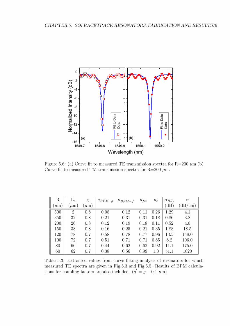
In chapter 5, we give all the measurement results on fabricated SOI racetrack
resonators. We demonstrated resonators of Q values as high as 119000 and finesse
values as high as 42. Compact resonators with radius of 20 µm resulting free
spectral range of 3 nm were also obtained. These devices operates as wavelength
drop filters. Thermooptical modulation and tuning of these resonator were also
studied. A resonator wavelength selective optical switch with low operation power
of 17 mW and high modulation speed of 210 kHz was realized. This is the
fastest SOI thermooptical device with no differential control. Finally, wavelength
add/drop filters based on a resonator of two bus waveguides were tested to have
crosstalk as high as 10 dB.
The thesis continues with chapter 6 which discuss the use of a layer trans-
fer method for SOI wafers and a set of devices realized with this method. So
far, all SOI integrated optical devices such as directional and multimode interfer-
ence couplers for beam splitting, thermo-optic modulators have been fabricated
through processing the top Si layer. However, it is clearly desirable to have the
capability to process both sides of the device for further electronic and/or optical
integration. Processing both sides of the silicon layer may result in novel devices
while improving performances of some of the existing ones. Transfer of the silicon
layer in SOI has recently been studied, but has not yet been used for integrated
optical device fabrication [52]. In this chapter we introduce the use of a layer
transfer method, which was successfully employed in GaAs-AlGaAs platform [53]
for SOI wafers. Such a layer transfer results in the possibility of using the back
side of the silicon layer in SOI structure for further processing. We developed
silicon-polymer waveguides, M-Z modulators, asymmetric vertical couplers with
this layer transfer method. Finally, the conclusion chapter summarizes all the
achievements and gives further suggestions.
Chapter 2
Tools of Integrated Optics
This chapter is devoted to the summary of basic physical principles and device
fabrication and characterization techniques. These principles and techniques were
implemented in the design and realization of integrated optical components dis-
cussed in this thesis work.
2.1 Basic Principles and Design
The basic components of integrated optics are planar optical waveguides. Slab
waveguides show light confinement in one of the transverse dimensions. One
will need rectangular waveguides when confinement in both of the dimensions is
intended. Light propagates in optical waveguides as modes. They are spatial
distributions of light during propagation. A waveguide can have single or multi
modes. Each mode of a waveguide has a different propagation constant or effective
refractive index.
12
CHAPTER 2. TOOLS OF INTEGRATED OPTICS 13
f
s
c
z
y
x
Figure 2.1: General slab waveguide structure with coordinate axis.
2.1.1 Slab Waveguides
Slab waveguides are known as the simplest of waveguides. Slab waveguides have
a minimum of three different layers (Fig. 2.1). For guidance of light, nf , refractive
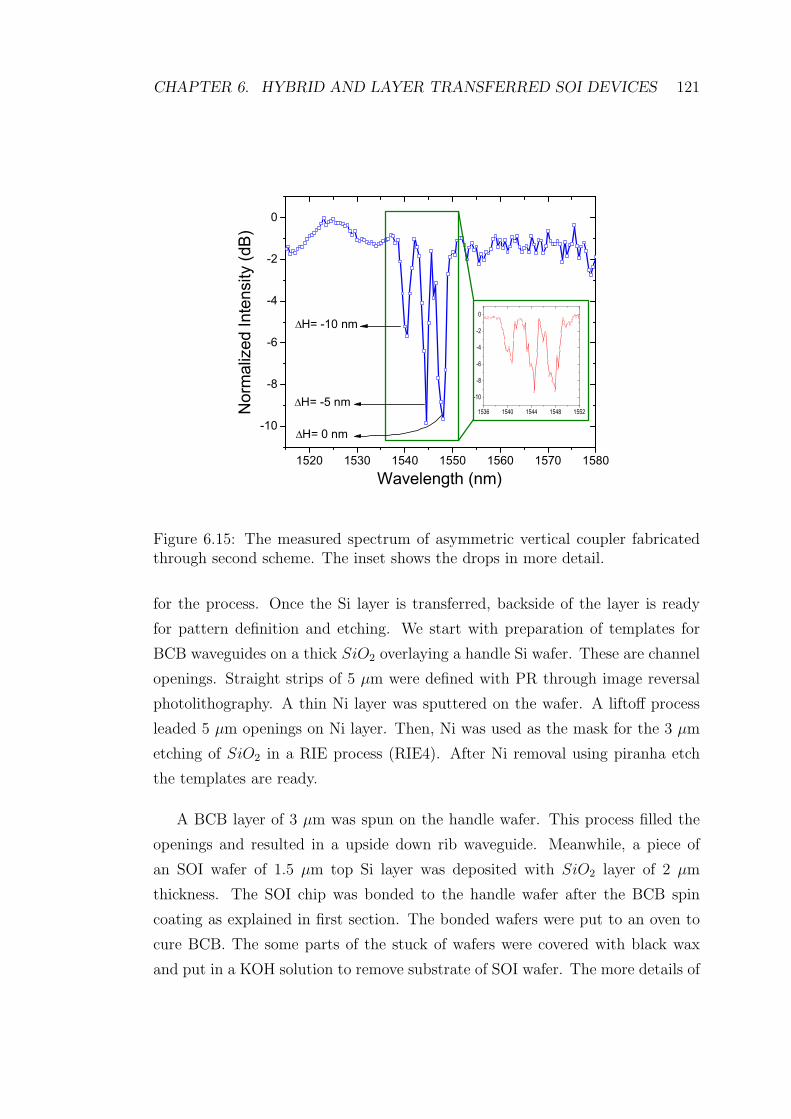
index of guiding film must be larger than nc, refractive index of cladding layer
and ns, refractive index of substrate layer,
nf > ns ≥ nc. (2.1)
The slab waveguide is said to be symmetric when ns=nc and antisymmetric
otherwise, ns 6= nc.
The slab waveguide supports a definite number of optical modes, and at least
one, if it is symmetric. These modes are calculated from Maxwell’s equations
through the application of boundary conditions. However, the same modes for
slab waveguides can be found by using ray optics concepts. Detailed discussion
of ray optics approach can be found in [54]. For a through analysis, one needs
to solve well known Maxwell equations for a source free (ρ=0, ~J=0 ), linear (ε
and µ are independent of ~E and ~H) and isotropic medium. Maxwell equations
are strongly coupled. They can be decoupled through a standard procedure of
creating a single second order differential equation. This procedure when applied
to the Maxwell equations leads to the wave equation, which is
∇2ψ − µε∂2ψ
∂t2= 0 (2.2)
CHAPTER 2. TOOLS OF INTEGRATED OPTICS 14
Figure 2.2: Graphical TE and TM solutions for a symmetric SOI slab waveguideof 1.5 µm thickness.
where ψ stands for either of ~E or ~H. After that, the wave equation should
be solved for the slab waveguide in Fig. 2.1. The parameters are chosen such
that nf > ns > nc and the guiding layer has thickness h. Rectangular cartesian
coordinate system are utilized to make the problem simpler. z is always chosen to
show propagation direction. There are two cases emerging from geometry, either
~E or ~H is parallel to the layer interfaces, which define TE or TM polarizations,
respectively.
The detailed slab waveguide analysis can be found in many textbooks [6] and
also in [54]. In summary, oscillatory fields are defined in terms of propagation
constants of the waveguide and frequency of light. Substitution of these fields into
wave equation and application of boundary conditions leads to so called eigenvalue
equation for propagation constant, β. The equation for TE polarization is
tan (hκf ) =γc + γs
κf [1 − γcγs
κ2
f
](2.3)
CHAPTER 2. TOOLS OF INTEGRATED OPTICS 15
The similar equation for TM polarization is
tan (hκf ) =κf [
n2
f
n2sγs +
n2
f
n2cγc]
κ2f −
n4
f
n2cn2
sγcγs
(2.4)
where γ and κ are defined as
Attaneuation Coefficient, γ =√
β2 − k20n
2 if β > k0n
Transverse Wavevector, κ =√
k20n
2 − β2 if β < k0n(2.5)
These equations are also called the characteristic equation of TE and TM
modes of a slab waveguide. They are transcendental equations and should be
solved numerically or graphically. These complex equations are simplified for the
special case of a symmetric waveguide. The eigenvalues of these equations, βTE
and βTM can be found for a slab waveguide with a definite thickness h and index
values for its layers using either a numerical or graphical software in a personal
computer as we did for a symmetric SOI slab waveguide of 1.5 µm thickness in
Fig. 2.2 [55].
2.1.2 Single Mode Rib Waveguides
The slab waveguide is easy to analyze and useful to understand the basic concepts
of optical waveguides. However, it has no lateral confinement and this reduces
the number of applications where it can be used. The alternatives are circu-
lar fibers and dielectric rectangular waveguides. The fibers are not compatible
with planar processing technology, such as planar chips, which are backbones of
integrated electronics. Light in a slab waveguide can be laterally confined and
resulting structure is the so called dielectric rectangular waveguide. The rectan-
gular waveguides have several geometric shapes leading to lateral confinement.
These shapes are rib, ridge, channel and diffused [54]. The optical waveguides
that we employed in this thesis are rib waveguides. The mode analysis of the
rectangular waveguides is a bit cumbersome and exact analytical solutions can
not be so easily found, instead, some simplified analytical results based on the
solution of the wave equation are further corrected by some perturbation tech-
niques. What is actually needed are some simple methods which will be useful
CHAPTER 2. TOOLS OF INTEGRATED OPTICS 16
s
f
f
s
f
s
air
s
f
eff1 eff1eff2
Figure 2.3: Effective index analysis for a rib waveguide of air cladding. (a) Therib waveguide with its critical dimensions. (b) Three slab waveguides constructedfrom the rib waveguide. (c) Artificially constructed slab waveguide using effectiveindex of three slabs.
CHAPTER 2. TOOLS OF INTEGRATED OPTICS 17
for design purposes. There are two basic waveguide design tools, namely effective
index method (EIM), which is a relatively easy method to apply and useful for
most of the design purposes and the beam propagation method (BPM), which is
a numerical simulation method. We generally designed our SOI rib waveguides
by EIM. BPM was used for fine tuning of the waveguide characteristics.
A rib waveguide can be analyzed using EIM as follows. A rib waveguide
can be divided so that three slab waveguide are formed as seen in Fig. 2.3.
The propagation constants of each slab are calculated from the characteristic
equations (Eqs. 2.3 and 2.4) of the slab waveguide for desired polarization. The
effective indices (neff1 and neff2) are calculated for each slab through
neff =β
k0
(2.6)
These effective indices are used to construct an artificial slab waveguide structure
as in Fig. 2.3. After that, calculation of the β is repeated for the new structure
using the equation for the orthogonal polarization and effective index is calculated
by Eqn. 2.6. The resulting effective index is the effective index of the original rib
waveguide.
Strictly single mode SOI waveguides requires sub-micrometer dimensions.
These waveguides are also called nanowire waveguides. They generally have
the same thicknesses of single mode SOI slab waveguides with values smaller
than 0.3 µm. Although nanowire waveguides allow us to construct very compact
devices, their very small dimensions lead to very high coupling losses between
the waveguide and a single mode fiber which has a diameter of 9 µm. On the
other hand, quasi-single mode waveguide propagation has been shown in SOI rib
waveguides with large cross section that is dimensions of a few µms [56]. These
waveguides have been used to realize many integrated optical devices that are
compatible with SM fibers. For these quasi-single mode waveguides, the single
mode condition which relates vertical and horizontal dimension of the waveguide
by facilitating EIM can be stated as
t < c+r√
1 − r2and r > 0.5 (2.7)
CHAPTER 2. TOOLS OF INTEGRATED OPTICS 18
Figure 2.4: Waveguide width (w) versus rib height (H-h) calculated from SMCapplied to SOI rib waveguides with oxide cladding. Results are shown for threedifferent waveguide heights (H).
where
t =weff
Heff
, r =heff
Heff
Details on how to find the effective width (weff ) and heights (Heff , heff ) can
be found in [54]. The relation in Eq. 2.7 leads to single mode propagation in
horizontal (lateral) direction while r > 0.5 ensures propagation of only one mode
in vertical (transverse) direction by avoiding deep etching of the waveguide. The
constant c was defined as 0.3 in [56]. It was calculated from an approximation
to a BPM simulation. However, it was later proposed that c values of 0 or -0.05
give better single mode condition for rib waveguide design purposes, [57].
The so called single mode condition given above can be used to design single
mode waveguides with large cross-section (H ≥ 3 µm). One can plot the equation
for specific waveguide heights. We did this for some representative height values
in Fig. 2.4. Such a plot may be more practical during fabrication of waveguides.
Although, the effective index method and the single mode condition may be found
CHAPTER 2. TOOLS OF INTEGRATED OPTICS 19
very practical, BPM simulations can give more accurate waveguide characteris-
tics. Therefore, verification of the number of modes and effective indexes should
be made by these simulations. We should note that these two methods are clearly
not sufficient for design of SOI rib waveguide with cross-section in the order of
1 µm. These waveguides have very interesting characteristics that would be im-
plemented in design of novel devices. We have used such waveguides in design
of several devices and mostly preferred to use BPM simulations for waveguide
analysis.
2.1.3 Beam Propagation Method
Unfortunately, analytical solutions are only available for a few simple waveguide
structures. There are also some approaches based on some approximation, like
effective index method that we discussed earlier. Most of the waveguide compo-
nents and devices are too much complicated to have neither analytical solutions
or be treated with approximation methods. Bend or tapered waveguides, y-
junctions or couplers are such kind of components. Beam propagation method
(BPM) provides numerical simulation of these components. It does not give ap-
proximate solutions. BPM can let us analysis even more complicated waveguides,
for example the refractive index or a geometrical property of the waveguide may
change along the propagation direction.
BPM simulates a structure by decomposing a spatial mode into superpositions
of plane waves using discrete Fourier transforms [6]. The mode is reconstructed
after the plane waves are travelled for a certain distance. Although BPM codes in
a numerical package can be used for simple one-dimensional structures, commer-
cially available BPM simulators should be used for fast analysis of more complex
2-dimensional structures. Polarization characteristics can also be studied with
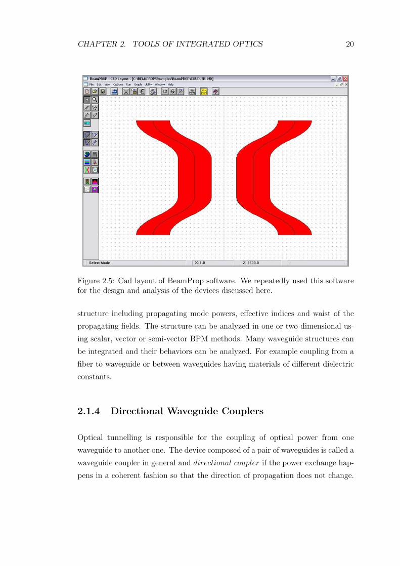
such simulators. We have used one of such simulators, BeamProp, for device
designs [58]. This software allows the user to define many structures compli-
cated in both geometry and index distribution in a cad layout (Fig. 2.5). An
assorted set of field profiles are available to be launched to the defined structure.
The software can also dynamically monitor many characteristics of the waveguide
CHAPTER 2. TOOLS OF INTEGRATED OPTICS 20
Figure 2.5: Cad layout of BeamProp software. We repeatedly used this softwarefor the design and analysis of the devices discussed here.
structure including propagating mode powers, effective indices and waist of the
propagating fields. The structure can be analyzed in one or two dimensional us-
ing scalar, vector or semi-vector BPM methods. Many waveguide structures can
be integrated and their behaviors can be analyzed. For example coupling from a
fiber to waveguide or between waveguides having materials of different dielectric
constants.
2.1.4 Directional Waveguide Couplers
Optical tunnelling is responsible for the coupling of optical power from one
waveguide to another one. The device composed of a pair of waveguides is called a
waveguide coupler in general and directional coupler if the power exchange hap-
pens in a coherent fashion so that the direction of propagation does not change.
CHAPTER 2. TOOLS OF INTEGRATED OPTICS 21
Figure 2.6: BPM analysis of a waveguide directional coupler. (a) X-Z contour mapof coupler. (b) Monitored optical power in each waveguide as light propagates inthe coupler.
Directional couplers are one of the fundamental waveguide devices used in inte-
grated optic circuits. They have been used in circuits designed for power splitting,
modulation or switching of light signals, wavelength filtering and polarization se-
lecting. A directional coupler consists of two identical waveguides very closely
placed, as in Fig. 2.6. The light incident at input of one of the waveguides
couples to the other as it propagates and full coupling of the optical power is
possible for long enough coupling length. Integrated optics uses coupled mode
formalism to handle directional couplers. Coupled mode theory can describe the
power exchange between all optical modes. When coupling occurs, the electro-
magnetic field propagating in a waveguide of a directional coupler is perturbed
by the evanescent tail of that of the other waveguide. The coupled mode theory
describes this perturbed field by superposition of unperturbed that is ideal modes
of the waveguide. The basic coupled mode theory has been constructed on the
scalar wave equation. What is computed with this method is coupling coefficient,
κ, for a directional coupler design. When κ is calculated, the length required for
CHAPTER 2. TOOLS OF INTEGRATED OPTICS 22
full coupling can be determined.
We have demonstrated the coupled mode theory approach for a directional
coupler with rib waveguide structure in [54]. Here we will give important results,
detailed calculation can be found there or in [6]. The optical powers in waveguide
A and B compromising a directional coupler exchange between each other. They
can be defined in terms of coupling coefficient, κ as
PA(z) = cos2(κz) (2.8)
PB(z) = sin2(κz) (2.9)
The total power goes back and forth between two waveguides and the driven field
(waveguide B) always lags 900 (See Fig. 2.6 for comparison). Using the above
equations we can write for lengths satisfying Lκ = π/2 + qπ complete energy
transfer occurs where q is an integer. This length can be extracted to be
L =π
2κ+qπ
κ(2.10)
The length for q = 0 is called as coupling length, Lc. Non-integer q values leads
couplings between 0 and 100 percent. κ (therefore Lc) is a strong function of g,
the gap between waveguides, w, the waveguide width H, the waveguide height,
h, the waveguide slab height and the refractive index difference between guiding
layer and substrate. That is, a coupling factor is very specific to a specific coupler
design. Therefore, coupled mode formalism may not be found practical enough
in designing a coupler. Waveguides generally bend to couple and decouple. An
effective coupling still takes place in these regions which brings further complexity
to the analysis. These bends may cause bending losses and change the effective
coupling constant and Lc. For these reasons, BPM has been used in all directional
coupler analysis made for polarization splitters, racetrack resonators, etc in this
thesis work. An example of coupler analysis using BPM is shown in Fig. 2.6.
2.2 Basic Fabrication Techniques
This section intends to give basic device fabrication procedures used in this thesis
work. These procedures are generally common for all devices. We give details of
CHAPTER 2. TOOLS OF INTEGRATED OPTICS 23
recipes and refer them later on in the thesis. Some devices need some uncom-
mon fabrication process and these processes are explained as these devices are
discussed in coming chapters.
Preparation of SOI samples for further fabrication processes, photolithogra-
phy, thin film deposition (dielectrics and metals) and etching etc. starts with
dicing of pieces from a whole SOI wafer. All the fabrication processes were done
in the class 100 facility of Department of Physics at Bilkent University. The
pieces cleaved out from SOI wafers have sizes depending the device designs. We
worked with chips with sizes ranging from 15x15 mm to 30x40 mm. Diced chips
are cleaned through tri-solvent cleaning which includes use of successive appli-
cation of trichloroethane (TCE), aceton (ACE) and iso-propanol (ISO) solvents.
Details of this cleaning technique can be found in [54]. Chips are rinsed under
running water for a while and blown with nitrogen then they are placed on a hot
plate at 110 0C for 1 minute in order to evaporate the remaining monolayer of
water on the chip surface.
2.2.1 Photolithography
We have used standard photolithography to transfer the device patterns from a
mask to a chip. Masks have clear and opaque parts defining the patterns. In
photolithography process, samples are first applied with some photoresist (PR),
then the aligner is used to align sample and the mask, then an UV light source is
used to expose the sample over the mask. After exposure, the samples are treated
with developer solvent. This solvent dissolves the PR parts which are exposed,
that is parts remained under the clear part of the mask during exposure, if the
PR is positive [59]. While PR on the other parts are dissolved in the case of a
negative PR.
The details of photolithography process done in our fabrication facility is as
follows. The samples are put on the spinning chuck of the spinner tool (Karl Suss
Model SM 120 Spinner) and a drop of 100 % HexaMethylDisilazene (HMDS)
solution is put on the sample surface to enhance the adhesion of the PR to the
CHAPTER 2. TOOLS OF INTEGRATED OPTICS 24
sample and the sample is spun at speeds ranging from 2000 to 6000 rpm for 40 s
so that HMDS is uniformly spread over the sample surface. We have used three
kinds of PR throughout the thesis work. They are AZ MIR701, AZ 5214E and
AZ TI35ES [60]. First one is a positive PR. The others can be processed as
either positive or negative. After covering all of the sample surface with drops of
a PR of our choice, the sample is once more spun at the same rate and duration.
The uniformly PR covered samples are prebaked on a hot plate at a temperature
around 100 C for a duration of about 50 seconds to strengthen the sticking of
PR to the sample and to solidify the PR. Actual bake temperature and duration
depends on the type of PR and given in the tabulated recipes for each PR (Table
2.1). The resulting PR film may have a thickness in the range of 0.75 to 3.5
µm. We can measure thicknesses after photolithography and developing steps
using Sloan Dektak 3030ST Surface Texture Analysis System. For both mask
alignment and exposure we used Karl-Suss MJB-3 HP/200W Mask Aligner. This
system uses a 500 W mercury xenon high pressure lamb as its light source and
in principle can define dimensions as small as 0.8 µm with 0.1 µm accuracy. The
mask is loaded on the mask holder of the aligner and the samples and patterns
on the mask are aligned such that the straight alignment marks on the mask are
parallel or perpendicular to the edges of the rectangularly cleaved samples. The
SOI samples used have surfaces on < 100 > plane and the strips are defined on
that plane also. Such an alignment may be critical especially if an anisotropic
etching (i.e. we used KOH for some device fabrications) is used later on. After
exposure, the exposed positive PR parts are dissolved in 25 percent aqueous AZ
400K developer solution and this results in realization of the mask patterns in
the PR film. When a negative PR is used, a second bake at 120 C for 2 mins
and a float (no mask) exposure of 1 or 2 minutes are required before application
of developer solution. The samples with PR patterns on their surface must pass
through another bake (called postbake) at 120 C for several mins if the patterns
are going to be used as a mask in an etching process. On the other hand, no
postbake is required if a thin metal film deposition and a liftoff process is used.
CHAPTER 2. TOOLS OF INTEGRATED OPTICS 25
PR Label AZ AZ AZ AZ AZ⇒ MIR701 5214E 5214E TI35ES TI35ES
Type of Use Positive Positive Negative Positive NegativeSpin Speed (rpm) 6000 4000 4000 5000 5000
Spin Dur. (s) 40 40 40 40 40Prebake Temp.(C) 90 110 110 100 100
Pressure (mTorr) 1000.0 1000.0RF power (W) 10.0 10.0
Temperature (0C) 250.0 250.0Grow Rate (A/mins) 400 100
Table 2.2: Recipes for growing Si3N4 and SiO2 films using PECVD
µm. Before deposition of metals, patterns are defined through photolithography
on the samples. Parts on which metal will be deposited should be clear, while
the other parts should be PR coated. Metal is deposited over all surface of the
sample, PR coated or not. After the deposition, the samples are put into a ACE
bath for a while. This is to facilitate the process called liftoff. ACE dissolves PR
film and lift the metal parts on PR off.
2.2.4 Etching Processes
Photolithography defines PR patterns onto surface of samples. PR layer should
be used as mask layer to transfer patterns into waveguide material or another
material that would be used as mask layer. Also patterns can be transferred to
metal layers through liftoff process as discussed above. PR layers or metal layers
are used as masking material in dry etching. On the other hand, Si3N4 is the
mask for KOH etch. We transferred PR patterns into Si3N4 through a dilute HF
etch. Before etching in HF solution, the PR patterns are further hardened via
another baking process at 120 for 2 mins at a hotplate. The HF solution that we
used was with the ratio 1 : 100 for HF (50%) : H2O. The etch rate 50 A/s. After
the etch remaining PR is removed in ACE. The sample with Si3N4 patterns are
ready for KOH etch.
Patterns must be defined into waveguide materials, to Si layer of SOI wafer in
our case. Dry and wet etching techniques can be employed for this purpose. In
both techniques, the unmasked parts on SOI samples are etched down for desired
CHAPTER 2. TOOLS OF INTEGRATED OPTICS 28
2
2
Figure 2.7: SEM micrographs of a SOI rib waveguide defined through KOHetching. (a) In topographic view of the waveguide facet, different materials canbe identified. (b) Normal SEM view of the same facet.
thickness. Dry etching uses physically assisted chemical radicals and ions, which
are produced in a plasma reactor, to etch the semiconductor material surface,
both chemically and mechanically. Dry etching which can be called as reactive
ion etching (RIE), results in an anisotropic etching profile. That is, some special
planes of semiconductor crystals are preferably etched at a higher rate than other
planes. On the other hand, wet etching being the most widely used etching
technique makes use of chemical reactions taking place between semiconductor
material and aqueous acidic and basic solutions. Unlike dry etching, wet etching
is generally isotropic for the most semiconductor material and etching solution
pair, but also some examples of anisotropic wet etchants exist. Both dry etching
(or RIE) [12, 32, 33, 34] and wet etching [23, 62] have been applied in silicon-on-
insulator based waveguide device fabrication.
Straight waveguides and devices that do not have circular or S-shaped parts
can be easily etched in anisotropic KOH etch. All the other shapes are better to
be defined through RIE. KOH anisotropic etching of silicon have been studied a
lot since the early 60’s [63, 64]. The etch rates are different for different KOH
CHAPTER 2. TOOLS OF INTEGRATED OPTICS 29
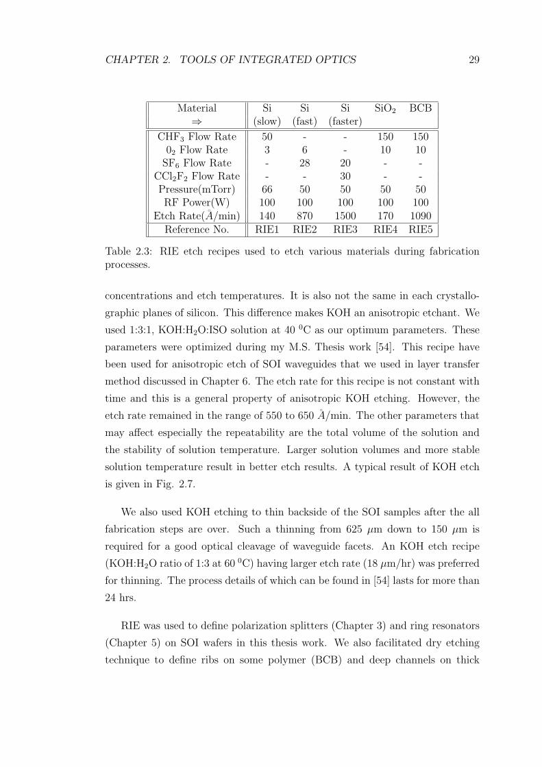
Material Si Si Si SiO2 BCB⇒ (slow) (fast) (faster)
Table 2.3: RIE etch recipes used to etch various materials during fabricationprocesses.
concentrations and etch temperatures. It is also not the same in each crystallo-
graphic planes of silicon. This difference makes KOH an anisotropic etchant. We
used 1:3:1, KOH:H2O:ISO solution at 40 0C as our optimum parameters. These
parameters were optimized during my M.S. Thesis work [54]. This recipe have
been used for anisotropic etch of SOI waveguides that we used in layer transfer
method discussed in Chapter 6. The etch rate for this recipe is not constant with
time and this is a general property of anisotropic KOH etching. However, the
etch rate remained in the range of 550 to 650 A/min. The other parameters that
may affect especially the repeatability are the total volume of the solution and
the stability of solution temperature. Larger solution volumes and more stable
solution temperature result in better etch results. A typical result of KOH etch
is given in Fig. 2.7.
We also used KOH etching to thin backside of the SOI samples after the all
fabrication steps are over. Such a thinning from 625 µm down to 150 µm is
required for a good optical cleavage of waveguide facets. An KOH etch recipe
(KOH:H2O ratio of 1:3 at 60 0C) having larger etch rate (18 µm/hr) was preferred
for thinning. The process details of which can be found in [54] lasts for more than
24 hrs.
RIE was used to define polarization splitters (Chapter 3) and ring resonators
(Chapter 5) on SOI wafers in this thesis work. We also facilitated dry etching
technique to define ribs on some polymer (BCB) and deep channels on thick
CHAPTER 2. TOOLS OF INTEGRATED OPTICS 30
SiO2
Si
Si
Si
Figure 2.8: SEM micrographs of some structures defined through RIE etching.(a) SOI rib waveguide etched using RIE1 recipe. (b) A silicon step etched usingRIE2 recipe.
thermally grown SiO2 layers. In principle, any type of material can be etched
down with a good choice of process gas. The critical point is to have a resistive
enough masking material. PR itself may be more than enough for shallow etches
as we did in fabrication of SOI polarization splitters and resonators. Etch depths
defined into top silicon layers were in the order of 0.5 µm. The use of thick PR
may help to reach etch depths up to 2 µm in silicon. On the other hand, it is
possible to define groves with depths larger than 4 µm using a 100 nm Ni layer as
mask. In the etching process of SiO2 layer, we define channels with depths of up to
4 µm with Ni as the masking material. We also used Ni mask to define grooves
with 6 µm depth on silicon chips which were then used as molds for analysis
of some biomaterials by Prof. Dr. Vasıf Hasırcı’s Group at METU. A specific
recipe is used when etching is performed in RIE systems. That is, gas flow rates,
chamber pressure and applied RF power are the parameters that determine etch
rate and anisotropy of a process. We tabulated the different recipes that were
used in RIE etching of various materials in Table 2.3 and referred to them later in
the coming chapters. Some SEM micrographes show results of some etch recipes
in Fig. 2.8.
CHAPTER 2. TOOLS OF INTEGRATED OPTICS 31
2.3 Basic Characterization Techniques
Fabricated devices are characterized on an integrated optics experiment setup.
In their characterization, devices are tested and results obtained are compared
with theoretical or design expectations. Waveguide as the basic component of
integrated optics, are characterized for their optical modal and losses properties.
The mostly applied tests to integrated optical devices are power splitting, wave-
length dependent transmission and power modulation due to an external effect.
An schematic view of our measurement setup can be seen in Fig. 2.9. We
have used both an external cavity tunable laser and a DFB (Distributed Feed
Back) laser as light sources. The tunable laser has wavelength resolution of ± 1
pm and can be tuned between 1515 nm and 1615 nm, while, the DFB laser lases
around 1550 nm. Optical measurements were generally performed with the laser
being at 25 0C and under 27 mA current. The laser has a peak value of 1547.58
nm under these condition. DFB laser was the light source during characterization
of polarization splitter and most of the other experiments that did not require
wavelength tunability. On the other hand, all the resonator (Chapter 5) and
asymmetrical vertical coupler (Chapter 6) tests need wavelength tuning and were
tested using the tunable laser.
Fiber-laser integration enables light to be transferred to a single mode (SM)
fiber with core size of 9 µm. This SM fiber is attached to another SM fiber which
is bent to form a number of circles with diameter of a few cm and placed in
three circular mounts called polarization controller and used to chose only one
polarizations state. The polarization controller is attached to another SM fiber
whose tapered and lensed (or optically cleaved) end is positioned in a fiber-chuck
on a piezoelectric XYZ translation stage. Submicron translation of input fiber
could be done by driving the stage with an external voltage supply. In butt
coupling, light is directly coupled into waveguides through the cleaved fiber end
or focused on waveguide facet when lensed fiber is used. Sample holder is also
integrated on a XYZ translation stage which improves the fiber-chip coupling.
Light coming out of the waveguides end facets is collected and then focused
to either a photodetector or an IR camera using a microscope objective. The
CHAPTER 2. TOOLS OF INTEGRATED OPTICS 32
IR Camera
Tunable or DFB Laser
Powermeter
Photodetector
Polarization
Controller
SM
Fiber
Translation
stages
GPIB
Cables Video
Cable
DUT
Data
Acquisition
PolarizerMicroscope
objective
Fiber
chuck
Figure 2.9: Schematic representation of experimental setup used for integratedoptical device characterization.
detector can measure output optical signal through the use of an oscilloscope or
optical powermeter. Optical power measurements are then used for calculating
optical losses. Fine positioning of optical modes were done using the camera prior
to any measurement.
A number of neutral density filters were used to control optical power to
avoid saturation of the camera when the images captured to image files using an
video capture card attached to a PC. Coupling properties of directional couplers
were calculated by analyzing captured IR images with an image contrast analysis
software. The software we used was labelled Scion Image and had the ability to
read relative intensities at each pixel of a straight line cursor placed on an image.
Tunable laser and powermeter were remote controlled through use of Labview
programming on a PC connected to the instruments by GPIB cables. We were
able to scan the laser wavelength in a range and with a resolution of our choice.
CHAPTER 2. TOOLS OF INTEGRATED OPTICS 33
2.3.1 Optical Waveguide Losses
Two types of optical losses that can be extracted from characterization of a
waveguide are insertion and propagation losses. First one include both losses
occurring during light propagation in the waveguide and those due to reflection
at input and output waveguide facets. The main contribution to propagation loss
comes from scattering of propagating light. Absorption of waveguide material
and radiation due to unguided modes are significant and are explained later in
this section. Scattering losses can result from imperfections in waveguide mate-
rial or on the surface of the waveguide. The material imperfections are voids,
crystalline defects and contaminant atoms and can be ignored for SOI optical
waveguides due to extremely pure nature of silicon crystal. On the other hand
scattering from waveguide walls can be an important source of loss and depends
on waveguide fabrication techniques. Since, light reflects many times from sur-
faces of a waveguide, it has been showed quantitatively that the surface scattering
loss depends on ratio of the roughness of the waveguide surfaces to the wavelength
directly, and the waveguide thickness and the amount of the tail of the evanes-
cent field. In the case of the SOI rib waveguides the roughness of the buried SiO2
layer, the thickness variation of the top silicon layer and the roughness of the
walls of the etched rib are the points to be considered. The first two are related
with the fabrication of the SOI substrate and they are results of the optimized
commercial technologies. The last is related with the etching of silicon during
fabrication process.
Absorption is a mechanism which is mostly important for semiconductor
waveguides. Band edge absorption and free carrier absorption are the two types
of absorption loss mechanisms that are dominant in semiconductor. We can safely
ignore losses due to band edge absorbtion since telecommunication wavelengths
(1.3 and 1.55 µm) are well apart from the band gap of the silicon (1.1 eV or 0.9
µm). We also eliminate free carrier absorption, fabricating devices on wafers with
low doping levels or high resistivity. Meanwhile, the radiation loss is the name for
the loss taking place when a waveguide design is near or beyond cutoff. Well con-
fined single mode waveguides do not suffer significantly from radiation. However,
CHAPTER 2. TOOLS OF INTEGRATED OPTICS 34
it should be considered for multimode and bending waveguides. In case of SOI
rib waveguides, radiation losses are not so significant as long as the waveguide is
designed as a single mode waveguide away from the cutoff.
The simplest way of loss measurement for SM waveguides is to input some
light with known optical power the waveguide and measure the optical power
at the output. While, prism-coupling loss measurement technique is generally
preferred for multimode waveguides [65]. What is measured for SM waveguides
is the insertion loss. Successive measurement of insertion loss for waveguides
of different lengths can be used to extract propagation loss of the waveguide.
Observation of Fabry-Parot resonances can also be used to determine propagation
loss [53]
The details of insertion loss measurement and extraction of propagation loss
are as follows. The light with a known wavelength and optical power is focused
or butt-coupled into cleaved or polished input facet of a waveguide using a from
cleaved or lensed SM fiber and the transmitted power is measured at the output
port. The insertion loss is calculated in dB’s using 10 log(Iin/Iout), where Iin and
Iout are the optical powers injected at the input and measured at the output, re-
spectively. This measurement is repeated for a large number of waveguides having
different lengths, but otherwise identical. This task is accomplished by starting
measurements with a relatively long (e.g. several millimeters) waveguide sample
then repetitively shortening the sample by cleaving. Measurements are repeated
for the waveguides of different lengths. The most important problem of this tech-
nique is with alignment which should be optimized for each waveguide/microscope
objective pair by maximizing output optical power. Then the logarithm of rel-
ative transmission is plotted with respect to waveguide length. The plot is a
straight line and its slope gives loss coefficient. This technique is effective for the
single mode waveguides which can be easily cleaved to optical quality. I used this
technique for loss measurement of 3 µm size during my Ms. Thesis work [54] and
found propagation losses of 0.70 and 0.76 dB/cm for TE and TM polarizations,
respectively.
A waveguide with optically cleaved facets can be considered as a Fabry-Perot
CHAPTER 2. TOOLS OF INTEGRATED OPTICS 35
Figure 2.10: Measured transmission spectrum of SM SOI waveguide. Fabry-Perotoscillations are used to calculate propagation loss of the waveguide.
interferometer. The facets behave as the partially transmitted mirrors of the
interferometer. An interference pattern forms with a change in the phase of the
propagating light. The phase change can easily be accomplished by tuning the
input wavelength. The measured optical power has maxima and minima with
scanned wavelength. The ratio of the maximum transmitted optical intensity to
minimum intensity can be defined as
Imax
Imin
=(1 +Re−αL)2
(1 −Re−αL)2(2.11)
in terms of reflectance of facets, R, optical power loss coefficient, α and cavity
length, L which is the length of the waveguide. Defining this ratio as κ, the loss
coefficient can be stated as
α =1
Lln[R
√κ+ 1√κ− 1
] (2.12)
The optical loss for a waveguide can be determined from Eq. 2.12 with the
knowledge of facet reflectance. In practice the same optical quality can not be
repeated in each cleavage of a waveguide sample so the reflectance of the facets
CHAPTER 2. TOOLS OF INTEGRATED OPTICS 36
can not be known exactly. In that case, the cut-back technique can be applied.
That is, measuring maximum and minimum intensity for waveguide samples with
the same features except different lengths. Then, 10log[(1+√κ)/(1−√
κ)] which
has dimension of dB, versus waveguide length is plotted. A straight line should
be fitted to that plot. The slope of the line gives optical loss coefficient and
extrapolated value to L=0 is the exact reflectivity of facets. We observed Fabry-
Perot oscillations for straight SOI rib waveguides of 1 µm size and found an upper
limit of 5.5 dB/cm for propagation loss. We used perfect reflectivity for Si facets
(Fig.2.10).
Chapter 3
Compact SOI Polarization
Splitters
In this chapter, design, fabrication and characterization of SOI directional cou-
plers utilized as a passive polarization mode splitter are explained in details. SOI
integrated optical directional couplers have already been fabricated [66]. How-
ever, they have not been exploited for polarization splitting applications. We
make use of birefringence accumulation in SOI rib waveguides as their sizes are
reduced. To the best of our knowledge, this device is the first integrated optical
polarization splitter based on SOI technology to separate light into TE and TM
modes.
In the next section, we explain the design and operation principles of the
device. Fabrication procedures and measurement techniques follow. Finally, the
experimental results and some analysis are given.
3.1 Splitter Design
The polarization dependent behavior of integrated optical waveguides has two
main sources. One source is the intrinsic material birefringence which can be due
37
CHAPTER 3. COMPACT SOI POLARIZATION SPLITTERS 38
Figure 3.1: Effective index difference between TE and TM modes of single mode(SM) SOI waveguides with h/H = 0.6. The insets show simulated fundamen-tal TE and TM mode profiles and effective refractive indices for the designedwaveguide.
to stress in the waveguides. The other source is due to waveguide geometry or
cross sectional profile. SOI single mode (SM) waveguides with large cross-section
are generally known for their polarization insensitivity due to inherent index
isotropy of the silicon crystal and negligible stress formed by wafer bonding. The
birefringence observed in these waveguides is negligible and has been attributed
to cross sectional geometry of the waveguides [12]. It has been shown by numer-
ical simulation that even the small birefringence in the rib waveguides can be
tailored to zero by adjusting the geometrical cross section [67]. However, as cross
sectional dimensions reduce, birefringence can increase and such waveguides can
be designed for a specific birefringence value. Analysis of SOI waveguides by 3D
vector beam propagation (BPM) simulations confirm the evolution of geometrical
birefringence in SM SOI waveguides as their size is reduced as seen in Fig. 3.1.
The waveguides with sizes w,H ≤ 1 µm display significantly different effective
indices for their TE (transverse electric) and TM (transverse magnetic) modes.
In our design, width (w) and height (H) of the SM waveguide is chosen to be 1
µm, while slab height (h) is 0.6 µm. These dimensions satisfy the single mode
CHAPTER 3. COMPACT SOI POLARIZATION SPLITTERS 39
C
2
SiO2
Air
H
W
hg
Figure 3.2: A schematic cross sectional view of coupling region of the designeddirectional coupler with critical dimensions.
condition for an SOI waveguide [56] and can be fabricated with good accuracy.
The inset in Fig. 3.1 shows TE and TM mode profiles for the chosen waveguide
structure.
In the light of this discussion, we design a directional coupler to be used as a
polarization splitter using SOI SM waveguides with top silicon layer thickness of
1.0 µm. For the preliminary design of the polarization splitter we first consider
the device layout shown in the Fig. 3.2(a) with its cross-sectional view given
in Fig. 3.2(b) . This is a straight directional coupler which can be analyzed
with minimal computational effort. Light is launched into port 1 and the output
power is detected either from port 2 or port 3. Optical propagation in a directional
coupler can be expressed in terms of even and odd modes of the coupled waveguide
system with effective indices ne and no. A directional coupler comprising two
single mode waveguide is said to have an odd and an even mode. The optical
field in the directional coupler at any instance can be expressed as a superpositions
of those modes [2]. The evolution of the effective index of these modes for TE
and TM polarizations are simulated and shown in Fig. 3.3 as a function of the
waveguide spacing. From the figure, it is clear that for small waveguide spacings,
the difference between propagation constants of the odd and even modes is large,
while they converge to the TE and TM effective indices of individual waveguides
as the spacing increases.
CHAPTER 3. COMPACT SOI POLARIZATION SPLITTERS 40
Figure 3.3: TE and TM effective indices of even and odd modes of a coupleras a function of waveguide spacing, g. Note that as g increases odd and evenpropagation constants converge to respective refractive indices of the isolatedwaveguides. The ratio of TM to TE coupling lengths are also shown.
(b) (c)
(a)C
TE TM
Figure 3.4: The schematic layout of the polarization splitter,(a) with 3D vectorBPM simulation results of a coupler with g=0.7 µm and Lc=110 µm for TE (b)and TM (c) modes. The simulations show the excellent polarization splitting. Gis 50 µm and the length of the S-bend is 3 mm.
CHAPTER 3. COMPACT SOI POLARIZATION SPLITTERS 41
The coupling length, Lc is the length necessary for complete energy transfer
and is different for TE and TM polarizations. The coupling length of either TE
or TM polarization is given by
Lc = (π)/(ne − no)k0 (3.1)
in terms of free space wavevector, k0. We seek a design where,
Lc(TM)/Lc(TE) = 2m (3.2)
relation is met. Here, m is an integer. The coupling length for TM polarization
becomes twice of that of TE polarization at a gap value of 0.8 µm allowing for
TE mode injected at the input port to couple back and forth and detected at
the output port 2, while the TM mode couples only once and is detected at the
output port 3. Using these values as a starting point we considered the design of
the polarization splitter shown in Fig. 4(a). In this case output waveguides are
separated at the output using S-bends. In order to take into account the coupling
contribution at the S-bend waveguides, full 3D vector BPM is used to obtain
the final design by scanning various waveguide spacings, g, from 0 to 1.5 µm.
Results of 3D vector BPM analysis show that gaps of 0.7 µm and 1.4 µm allows
polarization splitting with m values of 1 and 2, and Lc(TM) lengths of 110 µm
and 2450 µm respectively (Fig. 3.4(b)). The small difference between waveguide
spacing obtained from Eq. 3.2 (0.8 µm) and that obtained from BPM analysis
(0.7 µm) is due to the coupling contribution at the S bends. The corresponding
devices are the shortest possible polarization splitters with the chosen geometry.
3.2 Fabrication and Results
The SOI polarization splitters are fabricated so that the waveguide widths and
heights are 1 µm. Such small dimensions require very uniform silicon layer thick-
ness. Standard bond and etch back SOI (BESOI) wafers show thickness variations
of 500 nm which is not suitable for our purpose. However, Unibond wafers have
thickness uniformities ranging from ±20 nm down to ±5 nm [26]. These wafers
CHAPTER 3. COMPACT SOI POLARIZATION SPLITTERS 42
Figure 3.5: Cross-sectional SEM micrographs of (a)coupling region and (b)outputports. Optical images show (c)top view of coupling region and (d)cross-sectionalview of input port.
are fabricated by H+ ion implantation followed by heat treatment, while BESOI
wafers are bonded and polished down to the desired thickness.
We start the fabrication with a Unibond wafer with silicon layer thickness
of 1000 ± 20 nm and cleave a piece that has dimensions of 1.5 cm x 1.5 cm. A
photoresist layer is spun and the device is optically exposed by lithography (PL1).
The pattern is transferred to the SOI chip by reactive ion etching (RIE) using
a slow etch recipe (RIE1). The RIE etch is followed by the deposition of a thin
upper cladding layer of SiO2 using plasma enhanced chemical vapor deposition
(PECVD). In order to obtain optical quality facets for optical measurements, we
cleave the chip at the input and output ports. We find that best cleaves are
obtained when we thin the 625 µm thick substrate down to approximately 100
µm as explained in previous chapter. The optical and SEM micrographs of the
fabricated directional couplers are shown in Fig. 3.5.
The fabricated and optically cleaved devices are tested on the integrated op-
tics setup with a distributed feedback laser (DFB) laser operating at 1550 nm.
The input light polarization state is controlled by a fibre polarization controller.
In order to improve light coupling to the waveguides, a tapered and lensed fibre
CHAPTER 3. COMPACT SOI POLARIZATION SPLITTERS 43
Figure 3.6: Normalized polarized optical power measured at the output port 2 forboth TE and TM input signals for (a) gap=0.7 µm and (b) gap=1.4 µm. Linesare drawn to guide the eye.
with beam spot diameter of 2 µm was used. TE and TM measurements are made
separately. Before each measurement, the laser light optimized in either polar-
ization state is focused on the input facet of the directional coupler. A polarizer
with high extinction ratio is used after the device to confirm the polarization
state of the measured signal. The input waveguide connected to port 1 was at
least 3.5 mm from the point where the coupler starts to eliminate the possibility
of exciting both waveguides of the coupler while exciting port 1. Light at the
output ports are viewed by an IR camera and captured by a TV-video card. The
results for gaps of 0.7 and 1.4 µm are given in Fig. 5. We observe very good
polarization splitting at the designed coupling length of 2450 µm for 1.4 µm gap
(extinction ratios of 20.8 dB for TE and 9.7 dB for TM polarizations) and at
the designed coupling length of 120 µm for 0.7 µm gap (extinction ratios of 18.1
dB for TM and 8.0 dB for TE polarizations). Extinction ratios (ER) quoted are
defined in units of dB as
ERTE = 10log(P2
P3) (3.3)
CHAPTER 3. COMPACT SOI POLARIZATION SPLITTERS 44
for TE polarization and
ERTM = 10log(P3
P2) (3.4)
for TM polarization in terms of P2 and P3, optical powers measured at ports 2
and 3, respectively.
The results obtained from 3D vector BPM simulations and the results obtained
from the experiments are in very good agreement when the coupling contribution
from the S-bends is taken into account. The relatively large insertion losses due
to small cross sectional areas of these devices can be alleviated by using mode
transformers. Propagation losses of 5.5 dB/cm measured on straight waveguides
with same dimensions are in good agreement with the literature [51] and are due
to sidewall roughness and can be further reduced by controlled oxidation of the
waveguide surfaces [51]. These results prove that geometrical birefringence based
polarization control is possible in the thin core layers of SOI wafers. Even smaller
devices can be made using smaller gaps and smaller waveguide dimensions using
submicron core layers.
In conclusion, a SOI rib waveguide becomes birefringent as its size reduced.
We used this idea to design and fabricate a directional coupler polarization split-
ter based on geometrical birefringence. The device uses 1 µm sized silicon-on-
insulator waveguides. The length of the device is about 2500 µm for gap of 1.4
µm but is drastically shortened to about 120 µm for gap of 0.7 µm. We, thus
have demonstrated the first polarization splitter that uses geometrical birefrin-
gence control of high-index optical waveguides on silicon-on-insulator platform
[68].
Chapter 4
Ring/Racetrack Resonators:
Analysis and Design
This chapter gives analysis of ring/racetrack resonators and design of such res-
onators based on SOI rib waveguides. I explain basic waveguide resonator theory
in the first section then give design details in the second section. The chapter
concludes with a section analyzing possible integrated micro-ring resonators on
micromachined cantilevers to be used as a displacement sensor.
4.1 Analysis of Waveguide Ring/Racetracks
Resonators
A ring resonator system is composed of one or two straight waveguides called bus
waveguides and a ring placed very close to them as shown in Fig. 4.1. There
are several figures of merit for a ring resonator. These are the modulation depth
which shows the depth of the on/off ratio (in dB), free spectral range (FSR)
which is the wavelength spacing between adjacent resonances, full width at half
maximum (FWHM) of each resonance which shows how narrow the peak is at
the resonance wavelength. The Q factor gives the ratio of resonance wavelength
45
CHAPTER 4. RING/RACETRACK RESONATORS: ANALYSIS AND DESIGN46
Figure 4.1: Schematic representation of a single bus racetrack resonator and therelevant propagating field amplitudes.
to FWHM of the resonance. Depending on the application, large or small values
for FSR may be desirable but small FWHMs, large modulation depths and large
Q factors are always preferred.
4.1.1 Single Bus System
Consider the single bus coupled ring structure in Fig.4.1. The general matrix for
outgoing waves (Eo) in terms of incoming waves (Ei) in the coupling region of the
system can be written as [69]
Eo1
Eo2
Eo3
Eo4
=
0√
1 − κ 0 i√κ
√1 − κ 0 i
√κ 0
0 i√κ 0
√1 − κ
i√κ 0
√1 − κ 0
Ei1
Ei2
Ei3
Ei4
(4.1)
Here, κ is the fraction of power coupled between waveguide and ring, so that 1−κis the transmitted portion of the power that is not coupled to the ring. In the
case of no back reflections and Ei1 being the input wave,
Ei2 = Ei4 = Eo1 = Eo3 = 0 (4.2)
CHAPTER 4. RING/RACETRACK RESONATORS: ANALYSIS AND DESIGN47
Then, solving the matrix for the remaining terms leads to transmitted amplitudes
as
Eo2 =√
1 − κ Ei1 + i√κEi3 (4.3)
and
Ei4 =√
1 − κ Ei3 + i√κEi1 (4.4)
Matching the travelling waves in the ring gives,
Ei3 = Eo4 exp (−(αT
2+ iφ)) (4.5)
and using it to eliminate Ei3 in the above equations results in
Eo2 =
√1 − κ − exp (−(αT
2+ iφ))
1 −√
1 − κ exp (−(αT
2+ iφ))
Ei1 (4.6)
where, αT and φ are optical intensity loss and phase accumulated per round trip
in the ring, respectively. For a resonator of length, L = 2πR optical intensity loss
coefficient, α and effective refractive index of ne,
αT = αL (4.7)
and
φ(λ) =2π
λneL (4.8)
where λ is the free space wavelength. The resonance takes place when φ = 2πm,
and m is an integer number. Then, the resonance field amplitudes become
Eo2 =
√1 − κ − exp (−αT
2)
1 −√
1 − κ exp (−αT
2)Ei1 (4.9)
and
Eo4 =i√κ
1 −√
1 − κ exp (−αT
2)Ei1 (4.10)
An obvious result is that if
√1 − κ = exp (−αT
2) (4.11)
no power is reflected so that Eo2 = 0. This is the so-called critical coupling
condition and all the power is coupled to the ring.
CHAPTER 4. RING/RACETRACK RESONATORS: ANALYSIS AND DESIGN48
Figure 4.2: Phase dependence of transmitted power at the throughput port of asingle bus ring resonator system.
One has to take square of the field Eo2 and Eo4 to find the corresponding
optical intensities in terms of the input optical power. Therefore, the transmitted
power at the through port of single bus system is
Isb−thr = |Eo2|2 = |√
1 − κ − exp (−(αT
2+ iφ))
1 −√
1 − κ exp (−(αT
2+ iφ))
Ei1|2 (4.12)
The phase dependence of Isb−thr can be seen in Fig.4.2. FSR, FWHM and
modulation depth for this specific example are also shown in the figure.
4.1.2 Double Bus System
The above treatment can be easily extended to a ring structure coupled to two
bus ring structure as shown in Fig.4.3. When there is a second bus, there will
be a second coupling region allowing for the out coupling of trapped light in the
ring. The expression for transmitted power at through port is exactly the same
CHAPTER 4. RING/RACETRACK RESONATORS: ANALYSIS AND DESIGN49
Figure 4.3: Schematic representation of a double bus racetrack resonator and therelevant propagating field amplitudes.
as in the single bus system apart from a change in the loss term to account for
the coupled power to the second bus. The new loss term becomes
αeff = − ln (1 − κ2)1/2 +
αT
2(4.13)
Therefore, the transmitted intensity at the throughput port of double bus system
is given by
Idb−thr = |√
1 − κ− exp (−(αeff + iφ))
1 −√
1 − κ exp (−(αeff + iφ))Ei1|2 (4.14)
which can be simplified to
Idb−thr = |√
1 − κ1 −√1 − κ2 exp (−(αT/2 + iφ))
1 −√
(1 − κ1)(1 − κ2 exp (−(αT/2 + iφ))Ei1|2 (4.15)
To calculate the power at the drop port, the field, Eo8 in the output port can be
defined in terms of Eo4 as
Eo8 = i√κ2 Eo4 exp (−1
2(αT
2+ iφ)) (4.16)
CHAPTER 4. RING/RACETRACK RESONATORS: ANALYSIS AND DESIGN50
Figure 4.4: Phase dependence of transmitted power at the throughput port ofsingle bus system.
By taking square Eo8, the optical power at drop port can be calculated to be
Idb−drp = |√κ1κ2 exp (−(αT
2+ iφ))
1 −√
(1 − κ1)(1 − κ2) exp (−(αT
2+ iφ))
Ei1|2 (4.17)
The phase dependence of Idb−thr and Idb−drp can be seen in Fig.4.4 FSR,
FWHM and crosstalk (an other important characteristic of double bus system
and defined as the difference between measured intensities at throughput and
drop ports at a resonance) are also shown in the figure.
In above equations, κ1 and κ2 is the fraction of power coupled between the
resonator and the first and the second buses, respectively. In most cases κ1 =
κ2 = κ. However, analyzing the resonances and imposing that there is no reflected
power , i.e. Idb−thr = 0 , gives the critical coupling condition for the double bus
system as,√
1 − κ1 =√
1 − κ2 exp (−αT
2) (4.18)
CHAPTER 4. RING/RACETRACK RESONATORS: ANALYSIS AND DESIGN51
or
κ2 = 1 − (1 − κ1) exp (αT ) (4.19)
This condition defines an asymmetrically coupled resonator. κ1 should be large
enough to account for both resonator attenuation and coupling to the second
bus. It should be noted that the through port power is minimized and crosstalk
is maximized when this condition is satisfied.
4.1.3 Characteristics of Resonators
The basic characteristics of resonators are bandwidth (FWHM), free spectral
range (FSR), finesse, Q-factor and modulation depth can be extracted from their
responses. On the other hand, an analytical estimation can also be made for
these characteristics. An relation can be derived for FWHM from its definition,
the full width at half maximum ( Isb−drp=1/2 Iinp). Such a relation is ([70])
FWHM = ∆λ =λ2
0
πLneff
(1 − exp (−αT
2)√
(1 − κ))√
exp (−αT
2)(1 − κ)
(4.20)
This relation reduces to
FWHM = ∆λ =λ2
0κ
πLneff
(4.21)
when optical loss is negligible [71]. This relation suggests that smaller coupling
factors leads to narrower bandwidths. Furthermore, the accumulated phase of one
particular resonance (λ0) is 2πm and that of the successive resonance (λ0+FSR)
is 2π(m+1). The definition of accumulated phase can be used to calculate FSR
as
FSR =λ2
0
Lneff − λ0
(4.22)
which can be approximated as
FSR =λ2
0
Lneff
(4.23)
for large resonator circumferences. We can conclude from the above equation
that smaller resonators have larger FSR’s. From known FWHM and FSR one
CHAPTER 4. RING/RACETRACK RESONATORS: ANALYSIS AND DESIGN52
can easily calculate finesse and Q-factor as
Finesse =FSR
FWHM(4.24)
and
Q =λ0
FWHM(4.25)
,respectively. Physical meanings of finesse and Q-factor can be understood as
follows. The finesse equals to (to a factor of 2π) the number of round trips made
by light before the power in the resonator reduces to 1/e of the initial value.
Similarly, Q-factor is the number of field oscillations before field decreases to 1/e
of its initial value. Finally, the expected modulation depth (M.D.) of a resonator
can be calculated in the units of dB using resonance optical intensity at through
port as
M.D. = 10 log(Isb−thr(λ = λ0)
Iinp
) (4.26)
Apart from mentioned resonator characteristics, intensity enhancement in a res-
onator can be found interesting. Constructive interference occurred in a resonator
leads intensity to build up in the resonator. This feature of resonator is found
very helpful in nonlinear optics experiments in which high optical intensities are
required. For resonators with a single bus (all-pass configuration) the intensity
enhancement (I.E.) factor is given by ([71])
I.E. =1 +
√1 − κ
1 −√
1 − κ(4.27)
when resonator loss is negligible. The less coupling to a resonator leads more
intensity building up in the resonator.
4.2 Design of SOI Racetrack Resonators
The design of SOI resonators starts by determining the largest waveguide dimen-
sions that satisfy single mode condition. After a preliminary estimation using ef-
fective index methods, exact dimensions of the waveguides have been determined
after extensive numerical simulations using the three dimensional beam propa-
gation method (BPM). The waveguide has the same dimension of the waveguide
CHAPTER 4. RING/RACETRACK RESONATORS: ANALYSIS AND DESIGN53
Figure 4.5: (a) 3D to 2D reduction using effective index method for analyticalbending loss calculation for TE polarization. (b) 20 section of a bend definedfor numerical bending loss calculation using BPM.
used in polarization splitter design (Fig. 3.2). This is followed by the estimation of
the expected propagation losses which is critical in the design of high-Q waveguide
resonators. Measurements on straight waveguides designed and fabricated with
dimensions obtained in the simulation step, were performed to determine the up-
per limit on the expected propagation losses. In most Si rib waveguide devices,
quasi single mode waveguides with large cross sections are preferred to minimize
insertion losses. Design of ring resonators using SOI rib waveguides with typical
widths and heights of 3 µm or larger, however, leads to rings with radii larger
than 10 mm due to radiation losses at smaller radii. This would lead to poor free
spectral range. To obtain compact devices suitable for higher integration that
have larger free spectral range, ring resonators with curvatures of submillimeter
radii, are needed. Thus, smaller waveguide dimensions are essential for compact
ring resonators.
CHAPTER 4. RING/RACETRACK RESONATORS: ANALYSIS AND DESIGN54
Figure 4.6: Simulated and analytically calculated bending losses for 1 µm SOIwaveguide.
4.2.1 Bending Loss Calculation
A major issue in the design of ring resonators is the estimation of bending loss.
We first calculated the bending loss using a two dimensional analysis based on
Marcuse’s equation for bending slab waveguides. The details of the analysis
can be found in [72]. Briefly, in this approach, the 3-D waveguide structure
is reduced to 2-D (See Fig.4.5 (a)) using the effective index method, and the
resulting analysis leads to bending loss in dB’s for a given angular section ∆θ (in
radians) of radius R as
Lossbend = −10 log (exp (−αbend∆θR)) (4.28)
where αbend is the optical bending loss coefficient and is given by
αbend =α2
y
k30ne(1 + αy
w2)
k2y
(n2e2 − n2
e1)exp (αyw) exp (
−2α3y
3n2ek
20
R) (4.29)
The other variables are defined as
αy = k0(n2
e − n2
e1)1/2 (4.30)
CHAPTER 4. RING/RACETRACK RESONATORS: ANALYSIS AND DESIGN55
(a) TE (b) TM
Figure 4.7: SOI waveguide mode fields for TE (a) and TM (b) polarizations aftera propagation of 20 in a bend waveguide of 150 µm radius.
and
ky = k0(n2
e2 − n2
e)1/2 (4.31)
with k0 = 2π/λ0.
Alternatively, we also made use of 3D-BPM under wide angle approximation
conditions to simulate the bending loss by defining a 20 section of a bend shown
in Fig.4.5 (b) and calculating the bending loss by launching the computed mode
field of the straight waveguide into the curved section as explained in [72]. We
approximate the total bending loss for 90 by scaling the loss simulated for 20.
Both analytically calculated (Eq.4.28) and BPM simulated bending losses are
shown in Fig.4.6 for TE and TM polarizations. The results of both analysis show
that the bending losses drastically decrease for radii larger than 250 µm and 120
µm for TE and TM polarizations respectively. For a better visualization of light
propagating in an SOI bend waveguide, we show BPM calculated TE and TM
mode profiles after a propagation in a 20 bend of 150 µm radius in Fig. 4.7.
It is seen that after a 20 propagation a significant amount of TE mode field is
outside the rib of the waveguide. On the other hand, TM mode still propagating
under the rib. These results brings a more comprehensive explanation to the very
different bending losses for TE and TM polarizations.
CHAPTER 4. RING/RACETRACK RESONATORS: ANALYSIS AND DESIGN56
4.2.2 Coupling Factor Calculation
Following the determination of the range of radii that can be used in the design of
ring resonators, the coupled power factor from the bus waveguide to an adjacent
waveguide bend has to be calculated. 3D BPM simulations are also employed for
this purpose. A straight waveguide is placed close to a bent waveguide similar
to the one used to simulate the bending losses. The optical power launched
into the straight waveguide is monitored at the output of the bent waveguide
(inset of Fig.4.9). The minimum coupling gap is determined by the limits of
optical photolithography which, in our case, is 0.7 µm. This value limits the gap
coupling factor between the bus waveguide and the bent waveguide. To overcome
this problem and increase coupling factor for critical coupling, straight waveguide
sections are inserted into the bent waveguide sections in the coupling region next
to the bus waveguide. This transforms our design to a racetrack resonator. With
a coupling gap of 0.7-0.8 µm, the need for a racetrack shape becomes inevitable
as the ring radii gets smaller, since coupling factor is too small for smaller radii.
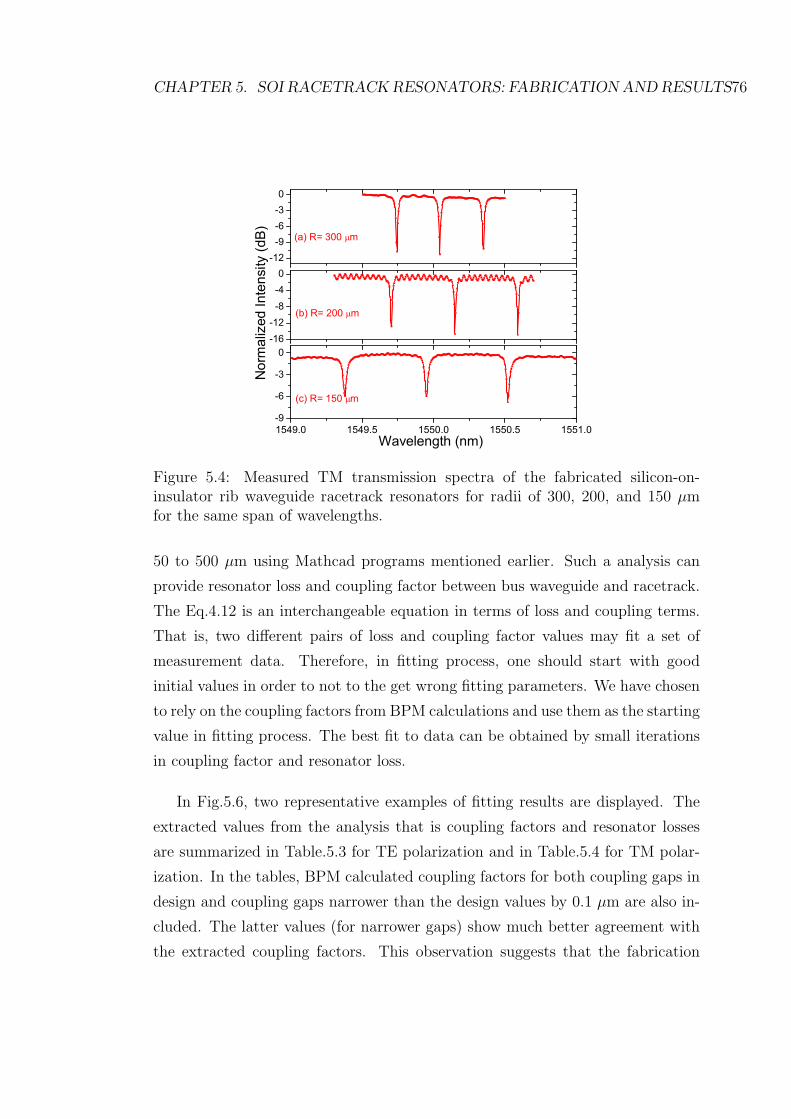
Output graphes of an coupling simulation is seen in Fig. 4.8. In the part (a)
of the figure, XZ contour map shows optical field in the coupling region of a
racetrack resonator. While the (b) part plots waveguide mode power as function
of propagation distance. The calculated coupling factors for a number of radius
as function of straight section length is given in Fig.4.9 for TE polarization. A
similar calculation was performed for TM polarized light input and the results are
plotted in Fig.4.10. A quick comparison shows that the TE coupling factors are
much more higher than those calculated for TM polarization for the same same
geometry. This is due to difference in the TE and TM mode profiles, which is also
responsible for the difference in calculated bending losses for both polarizations.
Using equations computed in previous section for optical intensities (Eqs.4.12,
4.15 and 4.17), and estimating total optical loss in the resonators, one can find the
necessary coupling factor. BPM results were used to find the gap and straight sec-
tion length that provide necessary coupling factor. The total optical loss includes
both bending and propagation losses. Bending loss is determined through analytic
calculation and BPM simulations as mentioned earlier, while the propagation loss
CHAPTER 4. RING/RACETRACK RESONATORS: ANALYSIS AND DESIGN57
Pathway 1
Pathway 2
Pathway 1
Pa
thw
ay 2
Figure 4.8: Output of a BPM simulation of coupling from a bus waveguide. Bendshave radius of 200 µm and straight section length and the gap are 48 and 0.8 µm,respectively.
Figure 4.9: Power coupled from bus waveguide to racetracks with various radiifor TE polarization as a function of straight section length for gap of 0.8 µm.
CHAPTER 4. RING/RACETRACK RESONATORS: ANALYSIS AND DESIGN58
Figure 4.10: Power coupled from bus waveguide to racetracks with various radiifor TM polarization as a function of straight section length for gap of 0.8 µm.
is experimentally measured on waveguides fabricated with same dimensions used
for the bus waveguides of the ring resonator system. We find the upper limit for
propagation loss to be 5.5 dB/cm (see Chapter 2).
Analytical results of the resonator analysis are used to write Mathcad pro-
grams to estimate the response of ring resonators. The programs let you to match
resonator loss with a coupling factor, iteratively. This is needed, since to match a
resonator loss with a coupling factor means increasing the straight section which
means an increase in resonator length and loss. Resonator characteristics of de-
signed resonator can also be extracted from the programs. A careful analysis is
made to match these values. The gap between bus and ring which is 0.8 µm is
large enough to print by photolithography and small enough to have reasonable
straight resonator section lengths. The designed resonators have bends with radii
ranging from 150 to 500 µm and racetrack shapes to increase coupled power from
bus waveguide.
The second gap for double bus ring resonator is calculated by matching two
coupling factors and the resonator loss which may be a greater deal. You may
CHAPTER 4. RING/RACETRACK RESONATORS: ANALYSIS AND DESIGN59
Figure 4.11: BPM simulation results for the design of tapers. The inset showsthe layout used for simulations.
Figure 4.12: The layout of the drown mask for SOI racetrack resonators.
CHAPTER 4. RING/RACETRACK RESONATORS: ANALYSIS AND DESIGN60
simply use the same value for the second gap (on drop port side) but a carefully
chosen asymmetric gap may result in better resonator responses. I chose the
second option in design of double bus resonators.
To increase the the coupling efficiency from single mode fibers to bus
waveguide we implemented tapers at the beginning and end of the bus waveguides.
The optimum taper design was obtained after a number of BPM simulations Fig.
4.11. According to simulations, a taper length of 200 µm is enough for optimum
coupling. We implemented a length of 1000 µm in the designed mask.
We included all the resonators designed in a mask. The L-edit software [73]
was used to draw the mask. Various values for bending radius and racetrack
straight section lengths and coupling gaps were included. The overview of the
drown mask is given in Fig.4.12.
4.3 Micro-Ring Resonators as Displacement
Sensors
(The work reported in this section was performed in collaboration with Mr. C.
Kocabas as a part of his Ms. Thesis [74].) During the design of the ring resonators,
potential applications were also considered. As a part of this effort, integration
of micro-ring resonators on micromachined cantilevers for displacement sensing
purpose was proposed and analyzed. These designed sensors may be used for
scanning probe microscopies [75].
Many scanning probe microscopies require the measurement of displacement
with high sensitivity. A good example is atomic force microscope (AFM) [76] ,
based upon the principle of sensing the forces between a tip and a surface. These
forces induce the displacement of the tip mounted on a cantilever. There is a
great need to determine the displacement of the cantilever with high sensitivity
to work out the attractive and repulsive forces between surface and the tip. There
are many methods to determine the tip displacement; these are tunnelling [76]
CHAPTER 4. RING/RACETRACK RESONATORS: ANALYSIS AND DESIGN61
Figure 4.13: A schematic illustration of the operational principle for the inte-grated micro-ring resonator displacement sensor, (a and c) shows the cantileverfor unbend and bend condition, (b and d) shows the field distribution on the ringresonator on the cantilever.
, optical lever [77] , interferometry [78] , piezo-resistive [79] and piezoelectric
detections [80] and interdigital detection [81] techniques. Integrated optical de-
tection method has many advantages over the others. First, an integrated sensor
does not require any alignment during the scanning of the surface and it is pos-
sible to scan large areas. Second, integrated sensors are suitable for cantilever
arrays due to their compactness, simplicity and potential for mass production.
It should also be mentioned that integrated sensors such as piezo-resistive ones
have less sensitivity than the external sensors such as optical levers. Using an
integrated optical sensor, it is expect to achieve as high sensitivity as external sen-
sors. Integrated optical devices can be inexpensive and they can be used in harsh
environments such as UHV systems and electromagnetically active environments.
Recently there have been many studies on the integrated optic pressure sensors,
bio-sensors, temperature sensors and strain sensors. These sensors consist of an
integrated optical device such as Mach-Zehnder interferometer [82] , directional
CHAPTER 4. RING/RACETRACK RESONATORS: ANALYSIS AND DESIGN62
Here, a new integrated optical sensor for scanning probe microscopes is pro-
posed (see Fig. 4.13). In this design, an optical waveguide coupled to a high
finesse micro-ring resonator integrated with a cantilever is used as a strain sensor
to deduce displacement. Basically, stress due to displacement of the cantilever
changes the local refractive index on the ring resonator through the photo-elastic
effect , and index change cause modifications in the transmission characteristics
of the optical waveguide coupled ring resonator. Monitoring the intensity modu-
lation trough the optical waveguide, it is possible to determine the cantilever dis-
placement with high accuracy. Finite Element Method (FEM) simulations were
carried out to get optimum sensor design and Finite Difference Time Domain
simulations (FDTD) are used to get the transmission characteristics of optical
waveguide coupled ring resonators. To achieve high sensitivity, different types of
ring resonators have been studied.
4.3.1 Physical Analysis
In the method employed in this work [85], a micro-ring resonator integrated on a
cantilever is used to measure displacement. The atomic forces make the cantilever
deflect from equilibrium and this deflection produces stress on the cantilever
surface. Index change on the ring due to the stress causes a shift in the resonant
wavelength. The stress reaches its maximum value at the supporting point of the
cantilever and it decreases linearly along the cantilever. Maximum stress on the
surface of the base of the cantilever as a function of tip displacement, z, can be
written as;
σmax =3Et
2l2z (4.32)
where E is the Young’s modulus of the cantilever material, t is the thickness, and
l is the length of the cantilever. Due to the photo-elastic effect, effective index
changes due to the stress and through the equation,
neff = n0 +∑
i
Ciσi (4.33)
where, Ci is the stress optic constant of waveguide and σi is the local stress.
For GaAs longitudinal and transverse stress optic coefficients are 1.7x10⁻¹¹ Pa−1
CHAPTER 4. RING/RACETRACK RESONATORS: ANALYSIS AND DESIGN63
1x10⁻¹¹ Pa−1, respectively [86]. Longitudinal stress is much larger than the
transverse stress, which can be neglected, so that
∆nmax ' Clσl '3ClEt
2l2z (4.34)
Change in refractive index can also be written as function of the force applied on
the tip. From Hooke’s law, force on the rectangular cantilever can be expressed
as
F = kz =wEt3
4l3z (4.35)
where k denotes the spring constant of the cantilever, then change in refractive
index can be written as,
∆nmax ' 6Cll
wt2F (4.36)
From Eq. 4.35 and 4.36, the refractive index change depends on the geometry of
cantilever and photo-elastic constant of the material. As the stress induced index
change is not uniform on the ring total accumulated round trip phase on the ring
can be written as,
∆Φ =2π
λ
∫
ring∆n dl ' 2πCl
λ
∫
ringσl dl (4.37)
where λ is the wavelength. In order to achieve large phase shifts, total length of
the ring must be kept large and the cantilever material with a large elasto-optic
coefficient must be chosen. A schematic illustration of the operational principle
for the integrated micro-ring resonator displacement sensor extracted from Finite
Difference Time Domain(FDTD) simulation is given in Fig. 4.13.
4.3.2 Waveguide Design
Although, it is possible to design the sensor for other material systems, we de-
sign and analyze ring resonators on GaAs/AlGaAs platform. The waveguides
designed are deeply etched to achieve strong confinement [87] , which is essential
to minimize waveguide bending losses. The general waveguide structure is seen
in Fig. 4.14(a). The fraction of Al, x, and the geometry of the waveguide are
chosen so that single mode propagation is assured. The basic limitation to the
resonator and therefore to the waveguide design is the need to propagate light
CHAPTER 4. RING/RACETRACK RESONATORS: ANALYSIS AND DESIGN64
Al0.6 GaAs0.4
nsubs=3
GaAsnair=1
w
Hnrib=3.372
(a) (b)
Ve
rtic
al D
ime
nsio
n (
µm
)
Horizontal Dimension (µm)
Figure 4.14: Single mode waveguide structure (a), and its mode distribution (b).
in a small radius of curvature of less than 25 µm with minimum loss, since a
typical cantilever width is about 50 µm. A few trials of BPM simulations with
different Al mole fraction and waveguide width, w, and height, H led us to a sin-
gle mode waveguide structure which can be fabricated using optical lithography.
This structure has 0.6 as x, 1 and 0.75 µm as w and H respectively. neff is 3.192
for TE polarization which is found by mode calculation using a commercial BPM
program (see Fig. 4.14(b)). Performed bending loss analysis (as done in previous
section for SOI waveguides) suggested that it would be safe to use an R value of
20 µm for the ring.
4.3.3 Ring Resonator as Displacement Sensor
For the purpose of sensing displacement, we are mainly interested in modulation
applications of ring resonators. It should be possible to obtain a large modulation
in transmitted optical power by small variations of the refractive index. This
kind of modulation is useful only if the resonance wavelength shift remains in
the bandwidth of the resonator. Such shifts can only be achieved through a
controllable change in optical path length of resonators, which is a function of
resonator physical length and effective refractive index. Here, stress induced
refractive index change is employed. When the ring resonator is designed to have
a high-Q factor, the modulation is dramatic due to steep fall of the transmission
CHAPTER 4. RING/RACETRACK RESONATORS: ANALYSIS AND DESIGN65
Figure 4.15: Longitudinal stress distribution on the cantilevers with a ring (a) anda race-track (b) shape resonator. Long straight arms in the race-track resonatorsare useful for increasing the accumulated phase shift.
dip. Transmission dips would be more stepper when resonators are designed to
work at the critical coupling regime.
As the operational principle of the ring resonator coupled waveguide sensor
depends on the stress distribution along the cantilever, we have calculated the 3-D
stress distribution using Finite Element Method (FEM) simulations, for which;
Young’s Modulus of 0.86 ×10¹¹ N/m2, and Poisson’s ratio of 0.31 were used.
Static stress analysis was performed using ANSYS [88] software. The mesh was
increased in the region where ring resonator was placed. The analysis performed
here uses the stress at the surface. The local stress on the top surface decreases
along the z direction and becomes negative on the opposite surface. Fig. 4.15
(a) shows the stress contours on the the ring resonator obtained from the FEM
simulation. Maximum stress occurs at the supporting point of the cantilever and
decreases linearly along the cantilever. From the figure, it is clearly observed that
large stress occurs on the two sides of the ring which are parallel with the major
symmetry axis of the cantilever. Calculated total accumulated phase on the ring
CHAPTER 4. RING/RACETRACK RESONATORS: ANALYSIS AND DESIGN66
with a radius of 20 µm is 5 × 10⁻⁴ rad for 100 A deflection of the cantilever.
In order to increase the accumulated phase shift, the parallel sides may be kept
longer. The optimum design is a race-track shaped resonator, because of its two
long parallel sides where stress is much larger than the curved sides. Fig.4.15
shows the stress contours on the race-track resonator. Stress distribution reaches
to its maximum value on the surface of the waveguide and decreases linearly
along its thickness. For the sensitivity calculations, we averaged stress along the
thickness of the waveguide. Average value of the stress is equal to the stress in
the middle of the waveguide where the intensity of the guided light is maximum.
As the stress distribution is calculated with the waveguides on the surface of
the cantilever, stress also varies along the width of the waveguides in the curved
sections of the devices. We neglected the variation of stress in the curved sections
and used the value of the stress in the middle of the waveguide in the calculations.
Phase shift can be approximated as;
∆Φ ' 3πClEtLrt
2λl2z (4.38)
where Lrt is the length of the race-track resonator. From the equation, it is
observed that the phase shift is linearly proportional to the cantilever deflection
and it is related to the cantilever geometry and mechanical properties of the
cantilever material. For higher sensitivity, total length of the ring and the elasto-
optic coefficient of the material must be large. Phase shift can also be written as
a function of force applied on the tip so that,
∆Φ ' 6πCllLrt
λwt2F (4.39)
where F is the applied force, w is the width of the cantilever. In order to increase
the phase shift due to the applied force we have to keep the length long and the
thickness of the cantilever small which results in a trade-off between force and
displacement sensitivity. It is not possible to achieve high displacement sensitivity
as well as high force sensitivity. We can conclude that short and thick cantilever is
sensitive to displacement measurements whereas long and thin cantilevers is more
sensitive for force detection. One interesting result which is seen from Eq. 4.39
is that the phase shift does not depend on the Young’s modulus of the cantilever.
For small displacements, output intensity is a linear function of displacement.
CHAPTER 4. RING/RACETRACK RESONATORS: ANALYSIS AND DESIGN67
Figure 4.16: Transmission spectrum of single bus and double bus race-track res-onators for both with (SBcr and DBcr) and without (SB and DB) critical couplingcondition, respectively. The increase in slope of the resonance when critical cou-pling is achieved is clearly observed.
4.3.4 Cantilever Design and Sensitivity Analysis
Fundamental mechanical parameters of an AFM cantilever are its spring con-
stant and resonant frequency. The optimal values of these parameters depend
on the mode of the operations, namely contact mode, non-contact mode, and
intermittent contact mode. GaAs has a large photo-elastic constant which makes
it a suitable material for fabrication of integrated optical devices and cantilever
[89, 90, 91]. Other materials such as Si3N4 and Si can also be used with varying
sensitivities. Our design is based on rectangular cantilevers which are compatible
with well established micromechanical fabrication technology. Typical microma-
chined cantilevers for AFM have lengths of 100 µm to 400 µm, widths of 20 µm to
50 µm and thicknesses of 0.4 µm to 10 µm. A large spring constant is preferable
for non-contact mode and intermittent mode operations. On the other hand, low
force constant is preferable for contact mode operations. The resonant frequency
is required to be a few kHz in order to minimize the external effects [92] .
CHAPTER 4. RING/RACETRACK RESONATORS: ANALYSIS AND DESIGN68
The sensitivity of displacement sensors is the essential property of the atomic
force microscopies. The minimum detectable force and the displacement depend
on the sensitivity of the sensor and the noise of the system. Integrated sensors
have less sensitivity than external ones. There have been several studies to in-
crease the sensitivity of the integrated sensor, but the best sensitivity achieved
so far is ∼10−6 A−1 [89] , which is two orders of magnitude less than the sen-
sitivity of the interferometric detection [78]. Force sensitivity can be defined as
the variation of the current on the detector per unit force applied on the tip and
with the same logic, displacement sensitivity can be defined as the variation of
the current on the detector per unit displacement of the cantilever. The current
on the detector is proportional to the light falling on it,
i =ηIthν
(4.40)
where η is the quantum efficiency of the photo detector, I0 is the incident optical
power, ν is the frequency of the light. Therefore,
∆i
i0=
∆I
I0(4.41)
The detected power, It depends on the transmission characteristics of the ring
resonator coupled waveguide. Transmission of the single and double bus ring
resonators are given in the Eq. 4.12 and Eq. 4.15, respectively. In Fig. 4.16,
we plot the transmission spectrum for a single bus and double bus resonators
with and without critical coupling condition. Achieving the critical coupling
condition, it is possible to have very high modulation depth and very narrow
spectral response. Output intensity variation with cantilever displacement is
given in Fig. 4.17. We can write displacement and force sensitivities as
Sd =∆ItI0∆z
=1
I0
dItdφ
dφ
dz(4.42)
and
Sf =∆ItI0∆F
=1
I0
dItdφ
dφ
dF(4.43)
In Table 4.1, we compare the calculated sensitivities of the ring resonators for
single bus and double bus configurations with and without critical coupling con-
dition. The highest sensitivities are achieved under critical coupling conditions.
CHAPTER 4. RING/RACETRACK RESONATORS: ANALYSIS AND DESIGN69
Figure 4.17: Transmitted intensity variation with cantilever displacement forsingle and double bus race-track resonator with (SBcr, DBcr ) and without (SB,DB) critical coupling condition achieved. The best results are obtained undercritical coupling condition.
The sensitivity of the ring resonator is wavelength dependent. Fig. 4.18 shows
the wavelength dependence of the race-track ring resonator. The most sensitive
operation can be achieved at the wavelength for which the output intensity has
the steepest slope. The calculated sensitivities are promising and it should be
possible to achieve sensitivities as high as the sensitivity of the interferometric de-
tection. Sensitivity of the detector depends mainly on the design of the resonator
and the waveguide. Considering the round trip losses, we design the resonator
to accomplish the critical coupling condition. To achieve critical coupling, gap
between straight waveguide and ring should be precisely controlled. In our de-
sign we estimate propagation loss to be on the order of 10 dB/cm for waveguides.
Under this condition, gap size for critical coupling should be lower than 0.1 µm
which can be defined by e-beam but not optical lithography. The solution for
optical lithographic fabrication would be to vertically couple the ring resonator
and the bus waveguide [45], for which coupling gap can be controlled precisely
through standard deposition or epitaxial growth techniques. But even if critical
coupling is not achieved, the calculated sensitivities are still very good, especially
CHAPTER 4. RING/RACETRACK RESONATORS: ANALYSIS AND DESIGN70
Figure 4.18: Sensitivity vs wavelength for single bus race-track case with criticalcoupling achieved.
for the double bus structure. In the double bus structure, the second bus can be
placed next to the ring but opposite to the first waveguide.
Table 4.1: Calculated displacement sensitivities for single and double bus ringresonator with (SBcr, DBcr ) and without (SB, DB) critical coupling conditionachieved.
In summary, a novel integrated ring resonator displacement sensor was pro-
posed for scanning probe microscopies. We design and analyze the feasibility of
the integrated optical sensor. The concept based on elasto-optic effect is dis-
cussed. The design of the ring resonator was described and theoretical investi-
gation of the force and displacement sensitivity was presented. The design of
GaAs based cantilever with integrated ring and race-track resonator have been
described in detail. We find that integrated optical sensor is attractive because
of its high sensitivity and simplicity. We introduce a new application area for
integrated optics. This design is a good alternative for piezoresistive cantilevers
CHAPTER 4. RING/RACETRACK RESONATORS: ANALYSIS AND DESIGN71
especially in electromagnetically active environments. Integrated sensors are suit-
able for cantilever arrays due to their compactness, simplicity and compatibility
with mass production. No need for alignment, compactness, and high sensitivity
are the main advantages of this method.
Chapter 5
SOI Racetrack Resonators:
Fabrication and Results
This chapter is devoted to realization of the resonators designed in previous chap-
ter and their characterization. There is no difference between resonators discussed
in following 3 sections in terms of fabrication. They are realized on SOI chips
following a fabrication sequence of optical photolithography (PL1), RIE (RIE1
or RIE2), SiO2 deposition in PECVD and silicon substrata thinning for better
cleavage as explained in Chapter 2. Fig. 5.1 summarizes the fabrication proce-
dure.
The chips were mounted in our integrated optics measurement setup. The
input optical signal was obtained from an external cavity tunable laser with a
resolution of 1 pm coupled to the straight bus waveguides using a tapered and
lensed fiber with a spot size of 2 µm. The polarization of the input light was
controlled by a fiber polarization controller before being coupled to the chip. An
infrared camera is used to align the fiber and the input facet. The light at the
output of the bus waveguide was collected with a microscope objective and passed
through a polarizer of high extinction ratio before reaching a Ge photodetector.
The transmitted optical powers were obtained as a function of wavelength.
The results for resonators and details of further fabrication processes if any
72
CHAPTER 5. SOI RACETRACK RESONATORS: FABRICATION AND RESULTS73
are given in the following sections along with detailed analysis.
5.1 High-Q Racetrack Resonators
The resonators results of which are given in this subsection are based on single
mode SOI waveguides of 0.42 µm rib height. The chip had a length of 7 mm
after cleavage. Optical micrograph showing one of the fabricated racetrack res-
onators is displayed in Fig.5.2. Single bus racetrack resonators of bending radii
ranging from 150 to 500 µm are characterized for both TE and TM polariza-
tions. The measured TE transmission spectra of some of fabricated resonators
are shown in Fig.5.3 for various bending radii measured at the throughput port of
the ring resonator system. A sample of spectra for TM polarization can be seen in
Fig.5.4. In addition to the sharp dips in the throughput spectrum, small ampli-
tude oscillations due to Fabry-Perot resonances between the ends of the straight
bus waveguide are clearly observed. The optical (including free spectral range
(FSR), full width at half maximum (FWHM), finesse, Q-factor and modulation
depth(M.D.)) as well as some physical characteristics of the resonators shown
in Fig.5.3 and Fig.5.4 are summarized in Table.5.1 and Table.5.2, respectively.
Q-factors of as high as 119000 were observed for both polarizations.
Racetrack resonators of bending radius smaller than 150 µ were also fabricated
with etch depth of 0.42 µm, to test level of validation of our bending loss esti-
mation. A set of measured spectra is given in Fig.5.5. The resonance dips smear
out for the resonators with R=120 µm bends for TE while resonance dips are ob-
served even for resonators with R=60 µm bends for TM polarization. We should
note that the resonator losses increase drastically for resonators with R=150 µm
and smaller radius for both polarizations. However, the increase is larger in the
case of the TE polarization. This should be a result of larger bending loss for TE
polarization in small radii bends.
To compare resonator round trip losses, one can curve fit Eq.4.12 to measured
spectra. I performed the fitting analysis for resonators of bending radii from
CHAPTER 5. SOI RACETRACK RESONATORS: FABRICATION AND RESULTS74
Si Substrate
SiO2
Si
1 µm
1 µm
Si
Lc
R
BusWaveguide
(a1)
Air1 µm
0.75 µm
(a2)
RacetrackResonator
PR
Si Substrate
SiO2
Si
1 µm
1 µm
Si
Lc
R
BusWaveguide
(c1)
Air
1 µm
0.42 µm
(c2)
RacetrackResonator
0.58 µmSi
Si Substrate
SiO2
Si
1 µm
1 µm
Si
Lc
R
BusWaveguide
(b1)
Air
1 µm
0.42 µm
(b2)
RacetrackResonator
0.58 µmSi
SiO2
0.9 µm
Figure 5.1: SOI rib waveguide racetrack resonator fabrication steps. Top andcross-sectional views are given. (a1,a2) Photolithography is used to transfer pat-terns to photoresist (PR), (b1,b2) Si layer is etched using RIE and remaining PRcleaned, (c1,c2) SiO2 is deposited using PECVD.
CHAPTER 5. SOI RACETRACK RESONATORS: FABRICATION AND RESULTS75
Figure 5.2: Optical micrograph of one of the fabricated racetrack resonators.Inset shows the coupling region.
Figure 5.3: Measured TE transmission spectra of the fabricated silicon-on-insulator rib waveguide racetrack resonators for radii of 500, 350, 200 and 150µm for the same span of wavelengths.
CHAPTER 5. SOI RACETRACK RESONATORS: FABRICATION AND RESULTS76
Figure 5.4: Measured TM transmission spectra of the fabricated silicon-on-insulator rib waveguide racetrack resonators for radii of 300, 200, and 150 µmfor the same span of wavelengths.
50 to 500 µm using Mathcad programs mentioned earlier. Such a analysis can
provide resonator loss and coupling factor between bus waveguide and racetrack.
The Eq.4.12 is an interchangeable equation in terms of loss and coupling terms.
That is, two different pairs of loss and coupling factor values may fit a set of
measurement data. Therefore, in fitting process, one should start with good
initial values in order to not to the get wrong fitting parameters. We have chosen
to rely on the coupling factors from BPM calculations and use them as the starting
value in fitting process. The best fit to data can be obtained by small iterations
in coupling factor and resonator loss.
In Fig.5.6, two representative examples of fitting results are displayed. The
extracted values from the analysis that is coupling factors and resonator losses
are summarized in Table.5.3 for TE polarization and in Table.5.4 for TM polar-
ization. In the tables, BPM calculated coupling factors for both coupling gaps in
design and coupling gaps narrower than the design values by 0.1 µm are also in-
cluded. The latter values (for narrower gaps) show much better agreement with
the extracted coupling factors. This observation suggests that the fabrication
CHAPTER 5. SOI RACETRACK RESONATORS: FABRICATION AND RESULTS77
Table 5.2: Characteristics of resonators for which measured TM spectra are givenin Fig.5.4 and Fig.5.5
procedure leads to narrower gaps than those in the design.
The extracted resonator round trip losses,αR.T. are plotted as a function of
resonator radius in Fig. 5.7(a). We can compare αR.T. shown in Fig. 5.7(a) with
calculated and simulated bending losses in Fig. 4.6. But, two notes should be
pointed out. One is that αR.T. is total loss in a resonator including bending and
scattering and material (if any) losses and the other one is that the calculated
bending losses in Fig. 4.6 are given for 90 bends. Keeping these points in
mind, one can easily realize the good agreement between the Fig. 5.7(a) and Fig.
4.6. The increase in αR.T. for smaller radii should be due to increase in bending
loss. Therefore, resonators with radii larger than 200 µm for TE and larger than
CHAPTER 5. SOI RACETRACK RESONATORS: FABRICATION AND RESULTS78
Figure 5.5: Measured TM and TE transmission spectra of the fabricated silicon-on-insulator rib waveguide racetrack resonators for radii of 40 to 120 µm.
CHAPTER 5. SOI RACETRACK RESONATORS: FABRICATION AND RESULTS79
Figure 5.6: (a) Curve fit to measured TE transmission spectra for R=200 µm (b)Curve fit to measured TM transmission spectra for R=200 µm.
Table 5.3: Extracted values from curve fitting analysis of resonators for whichmeasured TE spectra are given in Fig.5.3 and Fig.5.5. Results of BPM calcula-tions for coupling factors are also included. (g
′
= g − 0.1 µm)
CHAPTER 5. SOI RACETRACK RESONATORS: FABRICATION AND RESULTS80
Figure 5.7: The extracted (a) resonator round trip and (b)effective propagationlosses and (c) measured finesse values for TE and TM polarizations. The solidlines are to guide the eye.
CHAPTER 5. SOI RACETRACK RESONATORS: FABRICATION AND RESULTS81
Table 5.4: Extracted values from curve fitting analysis of resonators for whichmeasured TM spectra are given in Fig.5.4 and Fig.5.5. Results of BPM calcula-tions for coupling factors are also included. (g
′
= g − 0.1 µm)
150 µm for TM are bending loss free as we predicted during the design. Also
the extracted resonator loss graph proves our prediction of larger bending losses
for TE polarization at smaller radii to be correct. Another observation with
extracted αR.T. values is that resonators with lower αR.T. values have the higher
finesse value. This feature is shown in Fig. 5.7(a) and (b).
In the Table. 5.3 and 5.4, calculated coupling factors, κc that would be nec-
essary to achieve critical coupling for characterized resonators are also tabulated.
κc was calculated by Eq. 4.11 using extracted resonator losses from the fitting
analysis. As a function of resonator radius, calculated κc’s are plotted in Fig.
5.8. κc and κfit values are most close at radius of 200 µm for both polarizations.
That is for 200 µm resonators are closer to critical coupling condition than other
resonator. This conclusion can also be verified by a look at measured modulation
depths in Table 5.1 and 5.2. The highest modulation depths are 12.2 dB for TE
and 14.8 for TM polarizations which are measured for R=200 µm resonators.
As a conclusion for this section, we demonstrated resonators with quality
factors as high as 119000 for both polarizations. Furthermore, resonators have
finesse values larger than 28 for TE polarization and larger than 43 for TM
polarization. Using standard optical photolithography technology, the quality
factor values reported here are the highest Q values achieved in the SOI platform,
CHAPTER 5. SOI RACETRACK RESONATORS: FABRICATION AND RESULTS82
Figure 5.8: The extracted coupling factors from fitting analysis and coupling fac-tors necessary to meet the critical coupling for TM (a) and TE (b) polarizations.The lines are to guide the eye.
excluding submicron Si wire resonators [93, 94]. It is clear that we do not achieve
perfect critical coupling which would result in lower than maximum Q-factor [50],
while low coupling factor results in low extinction ratio. Our results show that
we reach a good compromise between good extinction ratios and high quality
factors.
5.2 Compact Racetrack Resonators
The realization of high-Q waveguide resonators were achieved as explained in
previous section. However, resonators with radii smaller than 120 µm showed
relatively poor characteristics. Therefore, we studied the possibility of fabrica-
tion of these compact resonators with better resonance characteristics. For this
purpose, very high bending losses for bends of smaller radii had to be reduced.
We attained this goal by increasing the rib height of SM waveguide from 0.42
µm to 0.5 µm. The analytic bend loss calculation results show that the bending
losses drastically decrease for radii larger than 30 µm and 80 µm for TM and
CHAPTER 5. SOI RACETRACK RESONATORS: FABRICATION AND RESULTS83
Figure 5.9: Analytically calculated bending loss for a 90 bend as a function ofbending radius. The waveguide has dimensions of w and H are 1.0 µm and h is0.5 µm. The calculated TE and TM mode profiles for the SOI waveguide is alsoincluded.
TE modes, respectively (Fig.5.9). The relatively small bending loss for TM when
compared to TE is due to stronger lateral confinement of the TM mode. Mode
profiles showing this feature can be seen in the inset of the figure. The effective
refractive indices are calculated to be 3.3546 and 3.3402 for TE and TM modes,
respectively.
A number of resonators of bending radii ranging from 10 µm to 120 µm were
characterized for both polarizations. The measured TE and TM transmission
spectra are given in Fig.5.10 and Fig.5.11, respectively. The resonance charac-
teristics are summarized in Table.5.5 for TE and in Table.5.6 for TM. The free
spectral range of 0.7 nm at 120 µm radius increases to 3.0 nm for 20 µm devices
for TM polarization. Resonances for resonators are washed out due to excessive
radiation loss with radius of 10 µm or smaller for TM polarization, while this
takes place for resonators with radius of 40 µm or smaller for TE polarization.
CHAPTER 5. SOI RACETRACK RESONATORS: FABRICATION AND RESULTS84
Figure 5.10: Measured TE transmission spectra of the characterized resonators.
CHAPTER 5. SOI RACETRACK RESONATORS: FABRICATION AND RESULTS85
Figure 5.11: Measured TM transmission spectra of the characterized resonators.
CHAPTER 5. SOI RACETRACK RESONATORS: FABRICATION AND RESULTS86
Table 5.7: Extracted values from curve fitting analysis of resonators for whichmeasured TE spectra are given in Fig.5.10. Results of BPM calculations forcoupling factors are also included. (g
′
= g − 0.1 µm)
CHAPTER 5. SOI RACETRACK RESONATORS: FABRICATION AND RESULTS88
Figure 5.13: (a) Resonator round trip loss (b) effective propagation loss and (c)finesse values for TE and TM polarizations
CHAPTER 5. SOI RACETRACK RESONATORS: FABRICATION AND RESULTS89
Table 5.8: Extracted values from curve fitting analysis of resonators for whichmeasured TM spectra are given in Fig.5.11. Results of BPM calculations forcoupling factors are also included.
plotted as a function of resonator radius in Fig. 5.13 (a) and (b). Extracted
resonator losses for TM polarization decrease dramatically for resonator of 50
µm radius and follow a horizontal line with increasing resonator radius. However,
resonator losses for TE polarization are high for radius smaller than 80 µm. The
difference between TE and TM resonator losses of radius smaller than 80 µm seen
in Fig. 5.13 (a) and (b) is due to higher bending losses applied to TE mode of
the SOI curved waveguide for small radii. This explanation agrees very well with
our analytical calculation for bending loss of the SOI waveguide with 0.5 µm rib
height given in Fig. 5.9. Furthermore, we plotted measured finesse values for
both polarizations in Fig. 5.13 (c). Comparison with resonator round trip loss
plot shows that the finesse values increase rapidly as resonator losses decrease.
Poor finesse values for TE polarization at smaller radius reach values higher than
15 for radius larger than 80 µm. The decrease in resonator losses shows itself also
as increase in Q-factors of the resonators for both polarizations.
In summary to this section, we demonstrated that it is possible to realize
SOI rib waveguide based racetrack resonators with radius as small as 20 µm
resonating TM polarized light [95]. We also showed TE polarized light resonances
in resonators with radius as small as 50 µm. Free spectral ranges of 3.0 nm, finesse
values of 18.3 and Q-factors of 32980 have been observed. This more compact SOI
resonators can become key components for silicon based integrated optical devices
CHAPTER 5. SOI RACETRACK RESONATORS: FABRICATION AND RESULTS90
and even can be more easily integrated with MEMS structures (diaphragms and
cantilevers etc.) for sensor applications.
5.3 Thermo-optical Tuning of SOI Resonators
Ring resonators are distinguished from other integrated optics components with
their high wavelength selectivity, a key issue for many device applications rang-
ing from wavelength multiplexers [45] to modulators [96]. Recently, high-Q res-
onator based modulators with significantly lower switching powers have become
an important alternative to Mach-Zehnder (M-Z) modulators. Ability to tune
the output wavelength is the first step to the development of devices for applica-
tions such as optical modulators and switches. Wavelength tuning capability is
also required to fine tune to the desired wavelength when the target wavelength
is not met during the fabrication process due to imperfections or material non-
uniformity. Electro-optical [96], thermo-optical [10] and all-optical [97] tuning are
the most commonly used mechanisms in device applications. Although electro-
optical effect can be implemented for fast tuning and switching on compound
semiconductors, due to inversion symmetry crystal silicon lacks an electro optic
coefficient and is, therefore does not lend itself to this mechanism. On the other
hand, silicon is known for its large thermo-optic coefficient [11]. Use of thermo-
optic effect in silicon devices is a simple, straightforward and cost-effective way
for applications requiring moderate modulation speeds.
In this section, we concentrate on thermo-optical tuning of high-Q racetrack
resonators on SOI rib waveguide of 1 µm size and their operations as low-power
optical switch.
Fig. 5.14 (a) shows schematic top view of the designed SOI resonator with
the metal heater and contact pads. Cross-sectional detail of the SOI waveguide
is shown in Fig. 5.14 (b). This SOI waveguide geometry optimized by beam
propagation method simulations have been experimentally proved to be single
mode. These low loss single mode rib waveguides have already been used in the
CHAPTER 5. SOI RACETRACK RESONATORS: FABRICATION AND RESULTS91
Figure 5.14: Schematic views showing critical dimensions. (a) Top view of theSOI resonator and (b) cross-sectional view of SOI rib waveguide.
demonstration of polarization splitters and high-Q racetrack resonators [68, 94].
All pattern definitions throughout the fabrication of SOI resonators and their
thermo-optical tuning elements were done with optical photolithography. Res-
onator patterns were defined on an SOI wafer which had a 1.00 µm top Si and
a 1.00 µm oxide layers on a 625 µm thick substrate. The patterns were trans-
ferred to silicon layer by an amount of 0.42 µm using an RIE process resulting in
smooth sidewalls [94]. The etch was followed by deposition of about 0.3 µm SiO2
passivation layer on the wafer using plasma enhanced chemical vapor deposition
at 250 C. The 0.12 µm thick nickel heaters and contact pads were then defined
through a process sequence comprising photolithography, metal sputtering and
lift-off steps. The optical micrographs of a finished resonator and its overlaying
metal heater are shown in Fig. 5.15.
We cleaved the wafer to a chip of 8 mm length. The measured transmission
spectrum of the resonator with radius of 400 µm, straight coupling section of 48
µm and coupling gap of 0.8 µm is given in Fig. 5.16. The simulated spectrum of
the resonator using Eq.4.12 is also plotted in the figure. We used BPM calculated
coupling factors as initial values in the simulation. After a few iterations coupling
factor of 0.45 and resonator loss of 1.57 dB was obtained. This is to be expected
since we have already shown in [94] that SOI rib bend waveguides with radius of
CHAPTER 5. SOI RACETRACK RESONATORS: FABRICATION AND RESULTS92
Figure 5.15: (a) Optical micrographs showing top view of a fabricated racetrackresonator and overlaying metal heater.
300 µm or larger do not suffer from radiation loss due to curvature. Scattering
from imperfections due to fabrication is estimated to be the source of the resonator
loss. The free spectral range can be determined to be 248 pm from the figure.
The resonator shows a good modulation depth of larger than 11 dB. The full
width at half maximum (bandwidth) can be extracted from the curve fit to be 40
pm. Using this value with resonance wavelength and free spectral range of the
resonator, we calculated a Q-factor of 38000 and a finesse value of 6.2.
The resonance wavelengths of a resonator are determined through the phase
term, φ of Eq. 4.12 and can be tuned by either changing the resonator circum-
ference, L or the effective index, ne. Silicon is known for its large thermo-optical
coefficient of 1.84x10−41/C which have been employed to realize modulators
on SOI wafers [11]. Thermo-optical modulation of effective refractive index is at-
tained by placing a metal heater electrode near the waveguide. High-Q resonators
have narrow bandwidths and can be tuned to off-resonance with lower electrical
powers [10]. After passive characterization of the resonator, we applied electrical
power to the contact pads using micro-probes. The heater is a 0.12 µm thick
and 3 µm wide nickel layer in the shape of a circular bend to assure maximum
overlapping of heat flow with optical field in the resonator. It is just above the rib
of the waveguide with only a 0.3 µm thick SiO2 in between (Fig. 5.14 (b)). The
CHAPTER 5. SOI RACETRACK RESONATORS: FABRICATION AND RESULTS93
Figure 5.16: Measured and simulated TE transmission spectrum of the fabricatedSOI rib waveguide racetrack resonator.
bend shaped heater spans an angle of 60. The 100 µm wide nickel contact pads
were also designed in circular shape. They are well separated from the heater
(Fig. 5.14(a) and Fig. 5.15). The pads and heater combination was measured to
have a resistance of 170 Ωs. The measured transmission spectra of the resonator
under applied power are shown for four different applied power values in Fig.
5.17(a). There is an obvious tuning of resonance wavelength with applied power.
We also plot the resonance wavelength shift as a function of applied electrical
power in Fig. 5.17(b). It can be deduced from the figure that a total of 57 mW of
electrical power is sufficient to scan the resonator over its full free spectral range.
In order to relate the effective index change, ∆neff required to shift a specific
resonance by ∆λ the following argument can employed. The resonance condition
requires that the round trip phase, φ should be an integer multiple of 2π, that is
φ = (2π/λ0)neffL = m2π (5.1)
If the effective index changes so does the resonance wavelength. If we follow the
same resonance m does not change. Therefore for two different effective indices
CHAPTER 5. SOI RACETRACK RESONATORS: FABRICATION AND RESULTS94
Figure 5.17: (a) Measured TE transmission spectrum as electrical power appliedto the metal heater. (b) Shift in resonance wavelength as a function of appliedpower.
we get two different resonance wavelengths such that
m2π = (2π/λ0)neffL = (2π/λ′
0)n′
effL (5.2)
This equation can be rewritten as
2π L(neff
λ0
− n′
eff
λ′
0
) = 0 (5.3)
which leads to
neffλ′
0 = n′
effλ0 (5.4)
One can define λ′
0 = λ0 + ∆λ and n′
eff = neff + ∆neff so that
neff (λ0 + ∆λ) = (neff + ∆neff )λ0 (5.5)
or
∆neff = (∆λ/λ0)neff (5.6)
If we set ∆λ = FWHM , we get
∆neff = (FWHM/λ0)neff = neff/Q (5.7)
CHAPTER 5. SOI RACETRACK RESONATORS: FABRICATION AND RESULTS95
where Q is the Q-factor of the resonator. This equation suggests that the required
effective index change for a FWHM shift in a resonance is inversely proportional
to Q-factor. This relation explains why higher Q-factors lead to lower tuning and
switching powers.
In our case, the heater does not have the same length as circumference of
resonator, L. Therefore we should modify Eq. 5.7, by defining L = L1 + LH . We
Table 5.9: Characteristics of add/drop filters for which measured TE spectra aregiven in Fig.5.20. Results for the filter TM spectra of which is shown in Fig. 5.21is also included at the last row of the table.
bus resonators shown in Fig.5.20 and 5.21 are tabulated for convenience in Table
5.9.
A better understanding of the filter characteristics can obtained through an-
alyzing the spectra by curve fitting the measured responses to the expected re-
sponses given in Eq. 4.15 and Eq. 4.17. As representative examples, we applied
this analysis two filters that were shown in Fig. 5.20 (c) and (f) with radii of
200 and 500 µm respectively. The filters are referred as filter 1 and filter 2 in the
rest of this section. Such an analysis yields coupling factors and resonator loss
values, as observed in previous sections. Coupling factors numerically calculated
using BPM were used as starting values for curve fitting. The results of the mea-
surements as well as the fit curves using the design equations are given in Fig.
5.22. We give coupling factors and resonator losses extracted from this analysis
in Table 5.10. Results of BPM calculations using the designed coupling gaps are
also included for comparison. The results displayed in the table suggests that
simulated and extracted coupling coefficients for 1 and 0.9 µm gap are very close.
However, the difference between simulated and extracted coefficients increase for
gaps of 0.8 µm. To understand this difference we performed BPM simulations for
coupling gaps narrower than the design values by 0.1 µm, which showed much
better agreement with the extracted values. This suggests that the fabrication
procedure leads to narrower gaps than expected as the gaps get smaller.
Greater resonator loss for filter 1 is estimated to be mostly due to higher
CHAPTER 5. SOI RACETRACK RESONATORS: FABRICATION AND RESULTS99
Figure 5.20: Measured TE transmission and drop spectra of the characterizeddouble bus resonators.
CHAPTER 5. SOI RACETRACK RESONATORS: FABRICATION AND RESULTS100
Figure 5.21: Measured TM transmission and drop spectra of the double busresonator with R=200 µm and Lc=72 µm.
Figure 5.22: Fit to the measured transmission and drop spectra about (a)λ0=1549.773 nm for R=200 µm and (b) λ0=1549.878 nm for R=500 µm usingthe analytic functions in Eq.3 and Eq.4.
CHAPTER 5. SOI RACETRACK RESONATORS: FABRICATION AND RESULTS101
Table 5.10: Coupling factors which are numerically (BPM) calculated and ex-tracted from fit to measured data (Fig. 5.22)
radiation loss for 200 µm. Scattering loss should also have a considerable contri-
bution to round trip loss of filter 1 because the propagating light in the resonator
is affected by waveguide sidewall roughness more as the waveguide curvature de-
creases. In the light of the fitting analysis and critical coupling condition, we
should note that resonator losses were overestimated for both device in the filter
design. The analytical model that we used for calculation of radiation loss may
not be precise enough, but its simplicity makes it a very useful tool for the design
of waveguide resonators. The crosstalk was determined to be -10.0 dB for filter 1
and -1.9 dB for filter 2. The better crosstalk of filter 1 shows that it is much closer
to critical coupling. We verified this conclusion by substituting extracted filter
characteristics into the critical coupling relation. Even more reduced crosstalks
can be achieved with a better fulfillment of the critical coupling condition. This
can be achieved with larger κ2 (a narrower gap) for both filters. Crosstalk of a
filter shows separation level of ports of the filter.
In summary to this section, wavelength add/drop filters based on asymmet-
rically coupled silicon-on-insulator high-Q racetrack resonators are fabricated,
characterized and analyzed. The resonators are realized using single mode large
cross-section SOI rib waveguides having bending radii ranging from 150 to 500
µm. The resulting filters show Q-factors as high as 51000 and relatively low
crosstalks of -10.0 dB which can be reduced even further by a better match of
critical coupling condition [101].
Chapter 6
Hybrid and Layer Transferred
SOI Devices
We discuss the use of a layer transfer method for SOI wafers and a set of de-
vices realized with this method in this chapter. First, the transfer of SM SOI
waveguides is studied in the first section. Then in the second section, the method
is applied to SOI M-Z interferometers to test the method further. Finally, asym-
metric vertical couplers (AVC) and their realization using a hybrid technology is
discussed.
6.1 Layer Transferred SOI Waveguides
In this section, the feasibility of the silicon layer transfer process of SOI for in-
tegrated optical purposes is tested. Two waveguide chips were prepared. Layer
transfer process is applied to one of the chip, while the other is labelled as con-
ventional and used for comparison purposes.
102
CHAPTER 6. HYBRID AND LAYER TRANSFERRED SOI DEVICES 103
2
2
Figure 6.1: Cross-sectional schematic view for (a) conventional SOI waveguide(b) Si-polymer waveguide
6.1.1 Waveguide Fabrication and Si Layer Transfer
The optical waveguides reported in this section (Fig. 6.1) were fabricated on a
SOI wafer with silicon layer thickness, H, of 5 µm and buried oxide layer thickness
of 1 µm. Waveguides are designed to be single mode with a width, w, of 5 µm
and slab height, h, of 2.5 µm. The initial fabrication process is the same for
both conventional and substrate removed waveguides. We cleave two pieces with
dimensions of about 1.5 cm x 1.5 cm from the SOI wafer. The term conventional
is used in the text for no applied substrate remove process. After the samples are
degreased by three solvent cleaning process a 2000 Si3N4 layer is deposited using
plasma enhanced chemical vapor deposition (PECVD) at 250 C. Photoresist
is used as the mask during optical lithography (PL2) defining the waveguide
patterns which are then transferred to the Si3N4 layer by a dilute HF etch. After
removing the photoresist mask in acetone, the samples become ready for wet
chemical etching in 33 percent potassium hydroxide (KOH) at 40 C. We add
isopropyl alcohol to the solution to get smoother side walls at a ratio of 1:3 [54].
After the KOH etch, fabrication of conventional SOI waveguides is finalized by
the deposition of a 1 µm upper cladding layer of PECVD grown SiO2, whereas,
the fabrication process for the waveguide sample to be transferred continues. The
SEM micrographs of fabricated SOI waveguides is given in Fig. 6.2.
CHAPTER 6. HYBRID AND LAYER TRANSFERRED SOI DEVICES 104
Figure 6.2: Sem images of KOH fabricated conventional SOI single mode largecross-section waveguides. The detailed inset image shows the smooth side wallsand deposited SiO2 layer.
A piece of silicon wafer slightly larger than that of the waveguide, which is
to be used as transfer substrate, and the sample with the waveguides are both
deposited with a very thin (about 500 A) PECVD oxide layer at 250 C. This oxide
layer promotes adhesion between silicon and benzocyclobutane (BCB) polymer.
First, BCB polymer is spun onto the waveguide sample and left in an oven at 210C under nitrogen environment until the polymer is partially cured, which takes
about 30 minutes. This first polymer spin is done to planarize the sample surface.
The edge accumulation of the polymer on the planarized sample during spin
process is removed by cleaving the edges of the wafer. This is followed by coating
the transfer substrate also with BCB and placing it on a hot plate set at 165 C.
The polymer shows low viscosity and flows at this temperature. The planarized
waveguide sample is placed on the transfer substrate with the waveguides facing
the polymer surface. The sample can be easily moved on the transfer substrate
to align the crystallographic axes of the two substrates. The resulting stack is
put into the oven at 250 C for 2 hours under nitrogen atmosphere to fully cure
the BCB [102].
CHAPTER 6. HYBRID AND LAYER TRANSFERRED SOI DEVICES 105
Figure 6.3: Schematic representation of the layer transfer process. a) Planariza-tion of waveguide sample with partially cured BCB. b) BCB coating of transfersubstrate. c) Stacking of waveguide sample and transfer substrate with full cureof BCB. d) Substrate and oxide removal for waveguide sample.
After the full cure, the stack is bonded to a handle wafer and all surfaces of
the stack except the backside of the waveguide sample are covered with blackwax.
The new stack is placed in a KOH solution at a ratio of 1:3 at 50 C and left
there until the Si substrate of the waveguide sample is totally etched away. Buried
oxide layer acts as an etch stop layer and is removed after the KOH etch by a
dilute HF solution. The silicon layer transfer is schematically summarized in Fig.
6.3. A polished flat silicon surface remains after oxide removal. After cleaning
the blackwax and detaching the handle substrate, fabrication of the Si-polymer
waveguides is over.
6.1.2 Waveguide Characterization
Both the conventional and the substrate removed (Si-polymer) waveguides are
optically cleaved and analyzed on an optical test setup using an external cavity
tuneable laser. The input light polarization state is controlled by a fibre polar-
ization controller. TE and TM measurements are made separately. Near field
CHAPTER 6. HYBRID AND LAYER TRANSFERRED SOI DEVICES 106
Figure 6.4: A representative Fabry-Perot oscillation. Insets show a SEM view ofSi-polymer waveguide facet and a far field image of Si-polymer waveguide mode.
image of guided modes are viewed on an IR camera. We tested the waveguides
for single mode guiding and conclude that both waveguides are single mode. The
waveguides are then tested for their propagation losses and compared. For this
purpose, we employ the Fabry-Perot interference method. The light at output
waveguide facet is monitored with a Ge photodetector. The wavelength of the
input light is scanned over a 1nm range around 1550 nm in steps of 5 pm. This
measurement process is performed for both polarization states. The output power
through the waveguide is plotted as a function of wavelength. These plots show
Fabry-Perot oscillations (Fig. 6.4). Using the minima and maxima of the oscilla-
tions with the reflectivity of Si, the propagation losses are calculated for both TE
and TM polarizations. The calculated average TE and TM propagation losses for
both the conventional SOI waveguides and the Si-polymer waveguides are given
in Table 6.1. Higher than expected losses are due to assumption of perfect facets,
which is very hard to get for silicon waveguides of this thickness [103] by cleaving.
In this study, we emphasize the comparison of losses between the conventional
waveguides and the transferred rather than the absolute values which can be
improved by chemo-mechanical polishing.
CHAPTER 6. HYBRID AND LAYER TRANSFERRED SOI DEVICES 107
TE Propagation Loss TM Propagation Loss(dB/cm) (dB/cm) )
Table 6.1: Measured TE and TM propagation losses for SOI and Si-polymerwaveguide.
The comparison of modal and loss characteristics of the both waveguides
clearly proves the feasibility of the silicon layer transfer process of SOI for in-
tegrated optical purposes. The use of a polymer as the bonding agent makes
the bonding of a processed (i.e. having thickness variations) surface to another
wafer possible by planarizing it. Finally, this process prepares the backsides of
the waveguides for further processing. The quality of the backside surface is
so high that many micro fabrication processes including photolithography, met-
allization and etching, can easily be performed. We believe that such a layer
transfer process is a promising way of high-level hybrid integration of waveguide
devices.
6.2 Layer Transferred Mach-Zehnder Ther-
mooptic Modulator
In this section we further test the layer transfer method by applying on a Mach-
Zehnder (M-Z) modulator fabricated on a chip of 30x20 mm. This process is
very difficult when compared to what was done with straight waveguides. The
M-Z had thin metal layers of 20 µm wide, which makes the layer transfer more
challenging.
There have been a lot of research to develop thermooptic modulators and
switches on SOI platform. This is mainly due to lack of electrooptic effect in
Si. Additionally, large thermooptic coefficient of silicon makes realization of cost-
effective modulators operating on SOI posiible. The devices realized operated
with switching powers on the order of a few hundred mW depending on device
CHAPTER 6. HYBRID AND LAYER TRANSFERRED SOI DEVICES 108
R=5cm
R=5
cm
1 cm0.23 cm
50 µm
w=3 µm
0.5 cm
Heater
Figure 6.5: Schematic top view of a M-Z modulator. The dimensions are for thestructure used in fabrication.
and heater length. Apart from being an extreme demonstration of layer transfer
method, we expect that use of layer transfer method on SOI M-Z modulators
should decrease the switching powers drastically.
6.2.1 Modulator Design
Waveguide M-Z interferometer is one of the basic integrated optic devices. The
device has a junction that equally separates the input light into two arms. These
are called 3-dB junctions. A top view of an M-Z interferometer with a Y-junction
is given in Fig. 6.5. The geometrical dimensions shown in the figure is those of the
modulator that we used in fabrication. This was an already available modulator
mask. We thank Nadir Dagli for providing us with that mask. The Y-junction
section has s-bends having radius of 5 cm and the M-Z arms are separated from
each other by 50 µm. These arms combine on a second junction. The light signals
at the arms interfere at the second junction. Phase of one or both the signals can
be altered through physical mechanisms such as thermooptic effect. Therefore
the output light shows an interferometric feature. The time dependence of input
field can be given by
Ein = E0 cos(ωt) (6.1)
where ω is defined as 2πc/λ in terms of free space wavelength. The optical field
at each arm is Ein/2. If phase of one of the arms is changed by an amount of ∆φ,
CHAPTER 6. HYBRID AND LAYER TRANSFERRED SOI DEVICES 109
the electric field at the output port becomes
Eout =E0
2[cos(ωt+ ∆φ) + cos(ωt)] (6.2)
Then, the optical intensity at the output becomes
Iout = |Eout|2 = E2
0 cos2(∆φ) = I0 cos2(∆φ) (6.3)
The optical intensity changes sinusoidally between a maximum and a minimum,
if the phase difference changes continuously. Therefore, M-Z interferometers can
be used as modulators or optical switches. The phase difference in a M-Z arm
is obtained through the use of a physical effect to locally change the effective
refractive index of the waveguide mode. The effects mostly used are electrooptic
and thermooptic as we discussed in the previous chapter. Here, we concentrate on
the use of thermooptic effect to modulate a M-Z interferometer. To employ this
effect, a thin metal heater of length LH is placed on one arm of the interferometer.
The phase change corresponding to the change (∆neff ) in effective index is defined
as
∆φ = (2π/λ0)∆neffLH (6.4)
In this equation, ∆neff is given as dneff/dT∆T in terms of thermooptical coef-
ficient of the material and the change in local temperature.
6.2.2 Fabrication and Results
The M-Z modulators were fabricated on the same SOI wafers used in previous
section (Si-polymer waveguides). We used an RIE process to define ribs on the
wafer instead of anisotropic KOH etching. This is due to S-bends used in M-Z
design. Nickel was used as a mask in the etch process. The Ni M-Z waveguide
interferometer patterns were formed on the wafer using an image reversal pho-
tolithography (PL3) followed by Ni sputter and lift-off processes. An amount of
2.35 µm was etched on the top silicon layer using SF6 and O2 gases (RIE2). This
is followed by a PECVD growth to deposit 0.3 µm SiO2 passivation layer on the
etched patterns. The Ni heaters and connections to contact pads were formed
with another Ni sputtering and liftoff after the second photolithographic step.
CHAPTER 6. HYBRID AND LAYER TRANSFERRED SOI DEVICES 110
PR PR
Si Substrate
SiO21 µm
5 µmSi
Air 3 µm
1.5 µm
Si Substrate
SiO21 µm
5 µmSi
Air
3 µmNi
Si Substrate
SiO21 µm
2.5 µm
Si
Air
3 µm
Si Substrate
SiO21 µm
2.5 µm
Si
Air
Ni
3.5 µm
Handle Si Substrate
Si Substrate
SiO21 µm
2.5 µm
Si
BCB
Handle Si Substrate
2.5 µm
Si
BCB
Handle Si Substrate
SiO2
2.5 µm
Si
BCB
Handle Si Substrate
SiO2
2.5 µm Si
BCB
PR PR
Ni
For
Electrical
Contact
Figure 6.6: Schematic fabrication steps of layer transferred SOI M-Z modulator.
CHAPTER 6. HYBRID AND LAYER TRANSFERRED SOI DEVICES 111
(a)
(b)
(c)
(d)
(e)
(f)
Figure 6.7: Optical micrographies taken during the fabrication of M-Zmodulator:(a)Y-junction after first photolithography (b) Ni heaters defined oneach arm (c) After planarization using BCB (d) Y-junction seen from backsideafter layer transfer. (e) Openings for electrical contact (f) Input waveguide facetafter cleavage.
The substrate removal process is the same as explained in the previous sec-
tion. After 525 µm thick substrate was removed, another 0.3 µm SiO2 layer was
deposited on the newly revealed backside of the top silicon layer. Large rec-
tangular holes were opened on the backside to form pads and connect them to
previously fabricated heaters. This process was done by successive RIE etches
of a SiO2 (RIE4), a Si (RIE3) and another SiO2 (RIE4) layer after a third pho-
tolithography (PL5). During, this process trenches of 10 µm wide were also
opened between arms of M-Z structures. A final photolithography (PL2) and
metal sputtering steps were performed to form Ni contact pads and finalized the
fabrication of substrate removed SOI M-Z modulators. The fabrication steps
are schematically summarized in Fig. 6.6. The optical microscope photos taken
during the fabrication process are given in Fig. 6.7.
The fabricated chip was cleaved and mounted on the experimental setup.
CHAPTER 6. HYBRID AND LAYER TRANSFERRED SOI DEVICES 112
Figure 6.8: Temporal response of the layer transferred M-Z modulator to a squaredrive voltage.
Light with wavelength of 1550 nm was launched into the input facet of M-Z
modulator. The light outcoupled from the output facet was monitored with a Ge
detector. The device showed an insertion loss of 11 dB. This value is expected
for SOI devices of 5x3 µm2 facets. Then, we touched the contact pads with
microprobes and applied electrical power. The pad and heater combination was
measured to have a resistance of 400 Ω. The modulation observed with a square
driving voltage with amplitude of 3.8 V and frequency of 100 Hz is given in
Fig. 6.8. Although, the modulator does not show perfect switching (30 %), it
has a significantly reduced Pπ as compared to usual SOI M-Z modulators. We
calculated a Pπ value of 36 mW which is five times lower than an modulator
fabricated by our group with the similar geometries [104].
We also tested the M-Z for its modulation speed. We increased the frequency
of the driving voltage and measured the modulation depth of the optical signal.
The measured data is plotted as a function of frequency in Fig. 6.9. The 3-dB
cutoff frequency of 65 kHz was observed. This value is expectable for an SOI
CHAPTER 6. HYBRID AND LAYER TRANSFERRED SOI DEVICES 113
Figure 6.9: Measured modulation response to frequency change of driving voltage.
M-Z modulator of that geometry [104, 9]. The modulation speed of SOI M-Z
modulator is not lowered by the layer transfer.
To summarize, we have applied a layer transfer method to an SOI M-Z modu-
lator successfully. The resulting chip is an demonstration of an hybrid technology.
The layer transferred SOI M-Z modulators was tested and observed to have simi-
lar temporal responses as ordinary SOI M-Z modulators with significantly reduced
Pπ. We should not that this is the first attempt demonstration of the feasibil-
ity of this approach. This method can be applied to M-Z modulators based on
SOI nanowires for flexible integrated optics circuitry. Such an application would
result in submiliwatt Pπ values [37].
CHAPTER 6. HYBRID AND LAYER TRANSFERRED SOI DEVICES 114
6.3 Silicon-polymer Asymmetric Vertical Cou-
pler
6.3.1 Coupler Theory and Design
Whenever two optical waveguides are close enough, light may leak from one to the
other through the coupling mechanism which is one of the mostly used physical
effects in integrated optical devices, such as couplers, splitters, modulators and
switches. The coupling between waveguides is generally analyzed by the coupled
mode theory, predictions of which agrees extremely well with experimental results.
In coupled mode theory, it is assumed that coupling changes the field amplitudes
of modes, while their propagation constants remain unchanged.
Consider two slab waveguides in Fig. 6.10. The guiding regions have different
refractive indices of n1 and n2 while all cladding regions are with index of nc.
This is an example for non-degenerate or asymmetric vertical coupler. We apply
the coupled mode theory to this structure. We will not derive coupled mode
equations and just make use of them. Derivations for these well known equations
can be found in many introductory optoelectronics books [5, 6]. The coupled
equations that relate the field amplitudes of the waveguide modes are
dA1
dz= −jκ
21exp(j∆βz)A2(z) (6.5)
anddA2
dz= −jκ
12exp(j∆βz)A1(z) (6.6)
here, the difference between propagation constants is given as
∆β = β1 − β2 (6.7)
and it is the measure of the phase mismatch. Also, κ21
and κ12
are coupling
coefficients and are
κ21
=1
2(n2
2 − n2
c)k2
0
β1
∫ h2+g+h1
h2+gε1(y)ε2(y)dy (6.8)
and
κ12
=1
2(n2
1 − n2
c)k2
0
β2
∫ h2
0
ε2(y)ε1(y)dy (6.9)
CHAPTER 6. HYBRID AND LAYER TRANSFERRED SOI DEVICES 115
2
c
c
2
zy
x
c
1 1
Figure 6.10: Two slab waveguides with different refractive index
for the mode fields ε1 and ε2. The energy conservation of the system requires that
the coupling coefficients should be equal. Thus for the waveguide mode fields
κ12
= κ21
= κ (6.10)
Applying the initial conditions, ie. A1(0) = 1 and A2(0) = 0, the equations
can be solved to give two oscillating solutions for A1(z) and A2(z). Then, the
optical powers are calculated by taking absolute square of the field amplitudes
and found to be
P1(z) = cos2(γz) + (∆β
2γ)2sin2(γz) (6.11)
and
P2(z) = (κ2
γ2)sin2(γz) (6.12)
where
γ2 = (∆β
2)2 + κ2 (6.13)
is the modified coupling coefficient when there is a phase mismatch.
The optical power exchanges between waveguides with the period π/γ. The
phase matching condition is achieved when the waveguides are identical, that is
∆β = 0. The distance required for full power exchange under phase matching
condition is
L0 =π
2κ(6.14)
CHAPTER 6. HYBRID AND LAYER TRANSFERRED SOI DEVICES 116
Figure 6.11: Power transferred as function of phase mismatch
However, the power transferred has very interesting behavior at the distance
L0 = π2κ
when there is a phase mismatch between waveguide modes. It shows a
diffraction like behavior and can be calculated using (6.12) and (6.13) to be
P2(L0) = (π
2)2sinc21
2[1 + (
∆βL0
π)2]1/2 (6.15)
where sinc(x) = sin(πx)/(πx) and the transmitted power is P1(L0) = 1−P2(L0).
The transferred power can be understood better by drawing (6.15) as a function
of ∆βL0 (Fig. 6.11). Phase mismatch, ∆β can also be written in terms of effective
index difference and free space wavelength as
∆β =2π
λ∆neff (6.16)
The coupled mode theory can be applied to a structure made of a low index
waveguide on SOI substrate. It has been shown that such devices are highly
wavelength selective [105]. In that case, n1, n2 and nc becomes indices of silicon
(∼ 3.5), a low index material (∼ 1.5), and SiO2 (∼ 1.46) respectively. If the
low index waveguide is single mode but silicon slab has several modes, which can
CHAPTER 6. HYBRID AND LAYER TRANSFERRED SOI DEVICES 117
Figure 6.12: Effective TE refractive index change with free space wavelength forhighest order mode (m = 6) of Si slab with SiO2 and air as lower cladding andSM BCB waveguide
be achieved by choosing h1 and h2 appropriately, it can be clearly seen that the
fundamental modes of silicon slab and the low index waveguide are never phase
matched. Therefore, no significant power coupling happens between fundamental
modes. However, the dispersion of the highest order mode of the silicon slab
waveguide (see Fig. 6.12 for the transverse electric (TE) mode) can be used
to phase match them with low index waveguide mode. A simple mode analysis
shows that fundamental mode has negligible dispersion compared to higher order
modes. Thus effective index, nsm of single mode low index waveguide can be
treated as constant. On the other hand, (Fig. 6.12) the highest order mode shows
a nearly linear behavior between two cut-off wavelengths and this dispersion can
be written as
n(λ) = nλoff1+mλ (6.17)
where nλoff1is the effective index at smaller cut off wavelength and m is the
associated slope in Fig. 3. Then, the effective index difference becomes ∆neff =
CHAPTER 6. HYBRID AND LAYER TRANSFERRED SOI DEVICES 118
n(λ) − nsm while phase mismatch is rewritten as
∆β =[nλoff1
+mλ− nsm]2π
λ(6.18)
Therefore, transferred power (6.15) can be analyzed in the wavelength domain
using (6.18).
What happens if a SM rib low index waveguide is placed instead of a slab
waveguide to take advantage of butt coupling with a SM fiber? The solution is
straight forward, mode analysis shows that mode dispersion of such a waveguide
is also nearly constant. Thus the modified transferred power equations (Eq. 6.15
with Eq. 6.18) can be used but nsm becomes effective index of the rib waveguide.
6.3.2 Fabrication and Results
We demonstrate an asymmetric vertical coupler by a hybrid integration of BCB
waveguides with Si slabs on the same wafer. We propose two integration schemes.
First is to define BCB waveguide on an SOI wafer through reactive ion etching of
BCB polymer. The other one uses channels opened in a thick SiO2 layer on a Si
wafer as waveguide templates for BCB and Si layer transfer. Although the first
scheme is simpler, the second one gives the opportunity of further processing of
the Si layer and would be useful for novel device applications. The summary of
the fabrication of asymmetric vertical coupler through the first scheme is shown
in Fig.6.13. A SiO2 layer of 2 µm was grown on a SOI wafer of 1.5 µm Si top
layer. BCB was spin coated to form a 6 µm thick layer. Then, the wafer was put
to the oven to cure the BCB. Straight PR strips of 6 µm width was patterned over
BCB layer using photolithography (PL2) and etched down (RIE5) to form a BCB
rib of 3 µm in height. A thick SiO2 cladding deposition ended the fabrication of
asymmetric couplers.
The fabricated wafer is cleaved to a chip of 10 mm in length and mounted
in the experimental setup. The input light from the tunable laser is scanned
from 1500 nm to 1580 nm an the light from output port of BCB waveguide is
monitored with Ge photodetector. The measured spectrum is given in Fig. 6.14.
CHAPTER 6. HYBRID AND LAYER TRANSFERRED SOI DEVICES 119
SOI Si Substrate
8 µm
Air
SiO2
Si
SiO2
1 µm
2 µm
1.5 µm
SOI Si Substrate
8 µm
Air
SiO2
Si
SiO2
1 µm
2 µm
1.5 µm
BCB 6 µm
SOI Si Substrate
8 µm
Air
SiO2
Si
SiO2
1 µm
2 µm
1.5 µm
BCB 6 µm
6 µm
PR
SOI Si Substrate
8 µm
Air
SiO2
Si
SiO2
1 µm
2 µm
1.5 µm
6 µm
6 µm
BCB
SiO2
3 µm
1.7 µm
Figure 6.13: AVC fabrication steps first scheme (a) A SiO2 layer is deposited onan SOI wafer of 1.5 µm top Si layer. (b) A BCB layer of 6 µm is spin coated onthe wafer. (c) Waveguide strips are photolithographically defined to PR. (d) Theunprotected BCB is etched down to define a rib. Finally a SiO2 cap claddinglayer covers the rib.
CHAPTER 6. HYBRID AND LAYER TRANSFERRED SOI DEVICES 120
Figure 6.14: The measured spectrum of asymmetric vertical coupler fabricatedthrough first scheme. The inset shows the drop in more detail.
The more detailed spectrum of the drop is given in the inset. An analysis of
the figure produces a bandwidth of 1.34 nm and an modulation depth of 13.2
dB. The analytic calculations and BPM simulations estimated bandwidths in
the order of 0.34 nm for a gap of 2 µm. The discrepancy can be explained as
follows. These calculations assumed perfect thickness uniformity. However, the
SOI wafer we used in fabrication has a Si layer with ± 20 nm thickness uniformity.
Strong dependence of the response of the coupler on the Si layer thickness and
its uniformity explains the increase in bandwidth.
Further BPM simulations showed that an decrease of 5 nm in thickness of Si
layer resulted in a blue-shift of nearly 5 nm in drop wavelength of the spectrum.
Therefore, the drop spectrum can be tuned by decreasing the silicon layer thick-
ness. We made use of this fact to realize a multi channel wavelength drop filter.
To realize such a device, we need to define and etch some parts of the Si layer.
This further process is impossible with the first fabrication scheme. However,
the second fabrication scheme which uses layer transfer method is appropriate
CHAPTER 6. HYBRID AND LAYER TRANSFERRED SOI DEVICES 121
Figure 6.15: The measured spectrum of asymmetric vertical coupler fabricatedthrough second scheme. The inset shows the drops in more detail.
for the process. Once the Si layer is transferred, backside of the layer is ready
for pattern definition and etching. We start with preparation of templates for
BCB waveguides on a thick SiO2 overlaying a handle Si wafer. These are channel
openings. Straight strips of 5 µm were defined with PR through image reversal
photolithography. A thin Ni layer was sputtered on the wafer. A liftoff process
leaded 5 µm openings on Ni layer. Then, Ni was used as the mask for the 3 µm
etching of SiO2 in a RIE process (RIE4). After Ni removal using piranha etch
the templates are ready.
A BCB layer of 3 µm was spun on the handle wafer. This process filled the
openings and resulted in a upside down rib waveguide. Meanwhile, a piece of
an SOI wafer of 1.5 µm top Si layer was deposited with SiO2 layer of 2 µm
thickness. The SOI chip was bonded to the handle wafer after the BCB spin
coating as explained in first section. The bonded wafers were put to an oven to
cure BCB. The some parts of the stuck of wafers were covered with black wax
and put in a KOH solution to remove substrate of SOI wafer. The more details of
CHAPTER 6. HYBRID AND LAYER TRANSFERRED SOI DEVICES 122
BCB curing and substrate removing is explained in first section. The transferred
Si layer was successively patterned to three parts and etched. A staircase like
pattern was resulted with 5-10 nm steps. A PECVD grown SiO2 layer finished
the fabrication process. The spectrum obtained from an AVC fabricated with
layer transfer method is shown in Fig. 6.15. Three independent drops are seen
in the spectrum as expected. However, the exact positions of dips are different
than the expected. The channels may not be fully filled with BCB. Remaining
air bubbles in the channel may change the effective index of the waveguide and
the position of dips.
In this section, we explained the physical principles behind operation of asym-
metric vertical couplers and fabricated and measured Si-BCB couplers with two
different fabrication schemes. These couplers may be used as wavelength filters,
detectors and sensors [105, 106]
Chapter 7
Conclusions and Suggestions
Silicon photonics which is a novel research field and getting more attraction among
researchers at both academic and industrial institutions is the main topic of this
thesis work. We have designed, fabricated and characterized a number of both
monolithic and hybrid integrated optical devices using silicon-on-insulator (SOI)
wafers. The devices were designed using both analytical calculation and numerical
simulations (beam propagation method, BPM).
So far researchers in the field of silicon integrated optics have been interested
on either large cross-section SOI or nanowire waveguides. Formers are good for
efficient coupling of light from a single mode fiber. Latter promise realization
of very compact devices needed for a dense integration on a single chip. Hov-
erer, SOI rib waveguides having dimensions of the order of 1 µm have become a
new branch of optical SOI waveguides [107]. These waveguides have sizes smaller
than the conventional large cross-section SOI waveguides (≥3 µm) but larger
than those of SOI nanowires (≤0.4 µm). Their geometrically controllable bire-
fringence may be very helpful for polarization diversity in SOI integrated optical
devices. We have used these waveguides to realize polarization splitters [68]. A
polarization-independent racetrack resonator [93] has also been realized using SOI
rib waveguides. Finally, we showed that dimensions not larger than 1 µm make
fabrication of high-Q resonators with radii as small as 20 µm possible [94, 95].
123
CHAPTER 7. CONCLUSIONS AND SUGGESTIONS 124
An SOI rib waveguide becomes more birefringent as its size is reduced. We
used this idea to design and fabricate a directional coupler polarization split-
ter based on geometrical birefringence. The device uses 1 µm sized silicon-on-
insulator waveguides. The length of the device is about 2500 µm for gap of 1.4
µm but is drastically shortened to about 120 µm for gap of 0.7 µm. The polar-
ization splitter is the first realized SOI integrated optical device that splits light
to its TE and TM parts [68].
We have carried an in depth analysis of optical waveguide ring and racetrack
resonators. Expected responses from one and two bus coupled resonators were
driven. Issues that should be considered during the design of resonators were
identified. We apply the analysis and design one and two bus coupled racetrack
resonators on SOI rib waveguides. The geometry of the waveguide was similar to
ones used in the design of polarization splitters. The bending losses and coupling
factors are the most important points when designing waveguide resonators. The
SOI rib waveguides used in the design were optimized for low bending losses. The
racetrack shape was preferred for better control of the coupling factor.
We have proposed a novel integrated ring resonator displacement sensor for
scanning probe microscopies. We designed and analyzed the feasibility of the
integrated optical sensor. The concept based on elasto-optic effect is discussed.
The design of the ring resonator was described and theoretical investigation of
the force and displacement sensitivity was presented. The design of GaAs based
cantilever with integrated ring and race-track resonator have been described in
detail. We find that integrated optical sensor is attractive because of its high
sensitivity and simplicity. We introduce a new application area for integrated
optics. This design is a good alternative for piezoresistive cantilevers especially
in electromagnetically active environments. Integrated sensors are suitable for
cantilever arrays due to their compactness, simplicity and compatibility with
mass production.
We have designed and fabricated SOI racetrack resonators and characterized
them. Resonators with quality factors as high as 119000 were demonstrated for
both polarizations. Furthermore, resonators have finesse values larger than 28
CHAPTER 7. CONCLUSIONS AND SUGGESTIONS 125
for TE polarization and larger than 43 for TM polarization. Using standard
optical photolithography technology, the quality factor values reported here are
the highest Q values achieved in the SOI platform, excluding submicron Si wire
resonators. The response of resonators were analyzed by fitting the analytical
functions. Resonator losses and coupling factors were extracted from the fitting
process. Losses increases as resonator radius decrease in accordance with expecta-
tions. Extracted coupling factors were compared with those obtained from BPM
simulations for various waveguide resonator gaps. Comparisons suggest that the
fabrication procedure emmployed in this study leads narrower gaps than those in
the mask. These high-Q resonators are suitable for applications such as quantum
optics.
We investigated the resonators using SOI rib waveguides further and a
waveguide structure with stronger light confinement was designed. We demon-
strated that it is possible to realize SOI rib waveguide based racetrack resonators
with radii as small as 20 and 40 µm for TM and TE polarized light, respectively.
Free spectral ranges of 3.0 nm, finesse values of 18.3 and Q-factors of 33000 have
been observed with the resonators based on new waveguide structure. This more
compact SOI resonators can become key components for silicon based integrated
optical devices and can even be easily integrated with MEMS structures (di-
aphragms and cantilevers etc.) for sensor applications. A good application for
these resonators is the realization of displacement sensosr that we proposed in
chapter 4. We have designed a mask and the fabrication of the sensor will be
done by a member of our research group in the near future.
We have studied the thermooptical tunability of resonators that we fabri-
cated. We also investigate possible use of such resonators as a wavelength selective
switch. Our measurements show that resonators show thermo-optical tunability
and operates as wavelength selective optical switches with low-power consump-
tion of 17 mW. The devices were tested to function as switches at frequencies up
to 210 kHz, the highest modulation frequency observed for SOI thermo-optical
devices to the best of our knowledge.
Two bus coupled resonators were also fabricated and characterized. They were
CHAPTER 7. CONCLUSIONS AND SUGGESTIONS 126
asymmetrically coupled to get better characteristics. These resonators functions
as wavelength add/drop filters, a key element for WDM systems. Their Q-factors
are limited by the coupling to the second bus waveguide. The resonators with
bending radii ranging from 150 to 500 µm were fabricated and characterized.
The resulting add/drop filters show Q-factors as high as 51000 and relatively low
crosstalks of -10.0 dB. The crosstalk value can be reduced even further by a better
match of critical coupling condition.
We have applied for the first time a layer transfer method to SOI wafers
for integrated optical applications. The transfer method was previously used in
GaAs/AlGaAs material system. To demonstrate the feasibility of the technique
we fabricated straight waveguides, Mach-Zehnder modulators, asymmetric ver-
tical couplers and hybrid silicon disk resonators. We optimized layer transfer
method for SOI wafers. In particular, wafer preparation, bonding, protection
during wet etching of silicon and the etching process were the steps that are
handled for optimization.
We have fabricated and compared SOI waveguides on two chips. One was
saved for comparison and the other was further processed for layer transfer. The
comparison of modal and loss characteristics of the both waveguides clearly proves
the feasibility of the silicon layer transfer process of SOI for integrated optical
purposes. The use of a polymer as the bonding agent makes the bonding of a
processed (i.e. having thickness variations) surface to another wafer possible by
planarizing it. Finally, this process prepares the backsides of the waveguides for
further processing. The quality of the backside surface is so high that many micro
fabrication processes including photolithography, metallization and etching, can
easily be performed. We believe that such a layer transfer process is a promising
way of high-level hybrid integration of waveguide devices.
Furthermore, we have applied the layer transfer method to an SOI M-Z mod-
ulator. This process differs from the one for SOI waveguides on two points. These
points makes the process even more challenging. First the area of transferred sili-
con layer is much larger and the the second the transfer layer have patterned thin
metal parts on the surface. The resulting chip was an demonstration of an hybrid
CHAPTER 7. CONCLUSIONS AND SUGGESTIONS 127
technology. The layer transferred SOI M-Z modulators was tested and observed
to have similar temporal responses as ordinary SOI M-Z modulators and with
significantly reduced Pπ, electrical power required for a phase difference of π. It
is also believed that integration of a thick layer of material having large thermal
conductivity (such as copper) may lead the device to operate at higher frequen-
cies. This method can be applied to M-Z modulators based on SOI nanowires.
Such an application would result in submiliwatt Pπ values.
We also analyzed asymmetric vertical couplers and their potential applica-
tions. These couplers include a low index single mode waveguide in close proxim-
ity of a high index multimode waveguide. The coupling generally occurs between
fundamental mode of the low index waveguide and the highest order mode of the
high index one. The fundamental modes show no dispersion while the higher or-
der modes does. The couplers are highly wavelength selective devices due to this
difference between the dispersion of the waveguides and their response strongly
depends on thickness of the layer with high refractive index. We fabricated and
measured Si-BCB couplers with two different fabrication schemes. These couplers
may be used as wavelength filters, detectors or sensors.
Finally, the research presented in this PhD thesis have resulted in five pub-
lished or accepted journal papers, three submitted papers and seven published
proceedings in technical conferences (see Appendix).
Bibliography
[1] G. Giesecke “Lattice Constants: Semiconductors and Semimetals 2”, New
York:Academic (1976).
[2] H. Nishihara, M. Haruna and T. “Suhara Optical integrated circuits”,
N.Y.:McGraw-Hill, (1989).
[3] R. Marz, “Integrated Optics”, Boston:Artech Hause, Inc., (1995).
[4] L. D. Hutcheson, “Integrated Optical Circuits and Components”, New
York:Marcel Dekker, Inc., (1987).
[5] B. E. A. Saleh and M. C. Teich, “Fundamentals of Photonics”, N.Y.:John
Wiley & Sons, (1991).
[6] Pollock C. R., “Fundamentals of Optoelctronics”, Chicago:Richard D. Irwin
Inc., (1995).
[7] A. Ozcan, M. J. F. Digonnet, G. S. Kino, F. Ay and A. Aydinli, “Char-
acterization of thermally poled germanosilicate thin films”, Optics Express,
12:20, (2004).
[8] A. Liu, R. Jones, L. Liao, D. Samara-Rubio, D. Rubin, O. Cohen, R. Nico-
laescu and M. Paniccia “A high-speed silicon optical modulator based on a