Date post: | 30-May-2018 |
Category: |
Documents |
Upload: | nguyenminh |
View: | 217 times |
Download: | 0 times |
PE46140Document Category: Product SpecificationMonolithic Phase & Amplitude Controller, 3.4–3.8 GHz
Features• 90° phase splitter
• 4-bit digital step attenuator, 7.5 dB range, 0.5 dB resolution
• 5-bit digital phase shifter, 87.2° range, 2.8° resolution
• High power handling and linearity
P0.1dB of +35 dBm
Input IP3 of +60 dBm
• 3-bit insertion loss stabilizer (ILS)
0.44 dB range, 0.06 dB resolution
• 32-lead 6 × 6 × 0.85 mm QFN
Applications• Wireless infrastructure
Macro cells
Small cells (micro, pico)
Distributed antenna systems (DAS)
• Precision phase shifter
• Dual polarization antenna alignment
• Analog linearization techniques
Product DescriptionThe PE46140 is a HaRP™ technology-enhanced monolithic phase and amplitude controller (MPAC) designed for precise phase and amplitude control of two independent RF paths. It optimizes system performance while reducing manufacturing costs of transmitters that use symmetric or asymmetric power amplifier designs to efficiently process signals with large peak-to-average ratios.
This monolithic RFIC integrates a 90° RF splitter, digital phase shifters and a digital step attenuator along with a low voltage CMOS serial interface. It can cover a phase range of 87.2° in 2.8° steps and an attenuation range of 7.5 dB in 0.5 dB steps, while providing excellent phase and amplitude accuracy from 3.4–3.8 GHz.
The PE46140 also features exceptional linearity, high output port-to-port isolation and extremely low power consumption relative to competing module solutions. It is offered in a 32-lead 6 × 6 mm QFN package.
The PE46140 is manufactured on Peregrine’s UltraCMOS® process, a patented variation of silicon-on-insulator (SOI) technology on a sapphire substrate, offering the performance of GaAs with the economy and integration of
Figure 1 • PE46140 Functional Diagram
RFIN
VDD
GND
SD
IC
LK LE
DSSDO
RFOUT2
-90°
0°
RFOUT1
SPENB
7.5 dB0.5 dB LSB
0 dB
87.2°2.8° LSB
87.2°2.8° LSB
Digital Interface
3Serial
Interface
©2015–2016, Peregrine Semiconductor Corporation. All rights reserved. • Headquarters: 9380 Carroll Park Drive, San Diego, CA, 92121
Product Specification DOC-64256-3 – (08/2016)www.psemi.com
PE46140MPAC
conventional CMOS. Peregrine’s HaRP technology enhancements deliver high linearity and excellent harmonics performance.
Absolute Maximum RatingsExceeding absolute maximum ratings listed in Table 1 may cause permanent damage. Operation should be restricted to the limits in Table 2. Operation between operating range maximum and absolute maximum for extended periods may reduce reliability.
ESD PrecautionsWhen handling this UltraCMOS device, observe the same precautions as with any other ESD-sensitive devices. Although this device contains circuitry to protect it from damage due to ESD, precautions should be taken to avoid exceeding the rating specified in Table 1.
Latch-up ImmunityUnlike conventional CMOS devices, UltraCMOS devices are immune to latch-up.
Table 1 • Absolute Maximum Ratings for PE46140
Parameter/Condition Min Max Unit
Supply voltage, VDD –0.3 5.5 V
Digital input voltage –0.3 3.6 V
Maximum input power 34 dBm
Storage temperature range –65 +150 °C
ESD voltage HBM(1), all pins 1500 V
ESD voltage CDM(2), all pins 1000 V
Notes:
1) Human body model (MIL-STD 883 Method 3015.7).
2) Charged device model (JEDEC JESD22-C101).
Page 2 DOC-64256-3 – (08/2016)www.psemi.com
PE46140MPAC
Recommended Operating ConditionsTable 2 lists the recommended operating condition for PE46140. Devices should not be operated outside the recommended operating conditions listed below.
Table 2 • Recommended Operating Condition for PE46140
Parameter Min Typ Max Unit
Supply voltage, VDD(1) 2.3 5.5 V
Supply current 350 500 µA
Digital input high 1.17 3.6 V
Digital input low 0 0.6 V
Digital input leakage 10 20 µA
RF input power, CW 29 dBm
RF input power, pulsed(2) 32 dBm
Operating temperature range –40 +25 +105 °C
Notes:
1) Product performance does not vary over VDD.
2) Pulsed, 5% duty cycle of 4620 µs period.
DOC-64256-3 – (08/2016) Page 3www.psemi.com
PE46140MPAC
Electrical SpecificationsTable 3 provides the PE46140 key electrical specifications at +25 °C, VDD = 2.3–5.5V, 50Ω, unless otherwise specified.
Table 3 • PE46140 Electrical Specifications at +25 °C
Parameter Path Condition Min Typ Max Unit
Operating frequency 3.4 3.8 GHz
Insertion loss RFIN to RFOUTXReference phase and minimum attenuation state. Includes 3 dB from power divider.
6.5 7.0 dB
Input return loss RFIN 3.4–3.8 GHz. All phase states. 15 dB
Output return loss RFOUT1 or RFOUT2 3.4–3.8 GHz. All phase states. 15 dB
Isolation RFOUT1 to RFOUT23.4–3.8 GHz.
Reference phase and minimum attenuation state.25.5 30 dB
Input 0.1dB compression
point(1) RFIN to RFOUTX 3.4–3.8 GHz. 35 dBm
Input IP3 RFIN to RFOUTX 3.4–3.8 GHz. 60 dBm
Switching time(2) 50% LE to 90% or 10% RF final value. 875 1220 ns
Phase shift range RFIN to RFOUTX 87.2 deg
Phase step 2.8 deg
Relative phase shift RFOUT1 to RFOUT2 Phase (RFOUT1)–Phase (RFOUT2) [same state]. –90 deg
Attenuation range RFIN to RFOUT2 7.5 dB
Attenuation step 0.5 dB
Notes:
1) The input 0.1dB compression point is a linearity figure of merit. Refer to Table 2 for the operating RF input power (50Ω).
2) Worst case state transition. All bits changing.
Page 4 DOC-64256-3 – (08/2016)www.psemi.com
PE46140MPAC
Table 4 provides the PE46140 key electrical specifications at +105 °C, VDD = 2.3–5.5V, 50Ω, unless otherwise specified.
Table 4 • PE46140 Electrical Specifications at +105 °C
Parameter Path Condition Min Typ Max Unit
Operating frequency 3.4 3.8 GHz
Insertion loss RFIN to RFOUTXReference phase and minimum attenuation state. Includes 3 dB from power divider.
6.5 7.8 dB
Input return loss RFIN 3.4–3.8 GHz. All phase states. 15 dB
Output return loss RFOUT1 or RFOUT2 3.4–3.8 GHz. All phase states. 15 dB
Isolation RFOUT1 to RFOUT23.4–3.8 GHz.
Reference phase and minimum attenuation state.22.5 30 dB
Input 0.1dB compression
point(1) RFIN to RFOUTX 3.4–3.8 GHz. 35 dBm
Input IP3 RFIN to RFOUTX 3.4–3.8 GHz. 60 dBm
Switching time(2) 50% LE to 90% or 10% RF final value. 875 1220 ns
Phase shift range RFIN to RFOUTX 87.2 deg
Phase step 2.8 deg
Relative phase shift RFOUT1 to RFOUT2 Phase (RFOUT1)–Phase (RFOUT2) [same state]. –90 deg
Attenuation range RFIN to RFOUT2 7.5 dB
Attenuation step 0.5 dB
Notes:
1) The input 0.1dB compression point is a linearity figure of merit. Refer to Table 2 for the operating RF input power (50Ω).
2) Worst case state transition. All bits changing.
DOC-64256-3 – (08/2016) Page 5www.psemi.com
PE46140MPAC
Switching FrequencyThe PE46140 has a maximum 25 kHz switching frequency.
The switching frequency is defined to be the rate at which the PE46140 can be continuously toggled across attenuation and phase states.
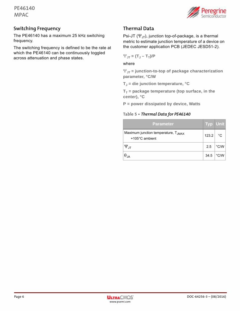
Thermal DataPsi-JT (JT), junction top-of-package, is a thermal metric to estimate junction temperature of a device on the customer application PCB (JEDEC JESD51-2).
JT = (TJ – TT)/P
where
JT = junction-to-top of package characterization parameter, °C/W
TJ = die junction temperature, °C
TT = package temperature (top surface, in the center), °C
P = power dissipated by device, Watts
Table 5 • Thermal Data for PE46140
Parameter Typ Unit
Maximum junction temperature, TJMAX
+105°C ambient123.2 °C
JT 2.5 °C/W
JA 34.5 °C/W
Page 6 DOC-64256-3 – (08/2016)www.psemi.com
PE46140MPAC
Control LogicTable 6–Table 11 provide the control logic truth tables for the PE46140.
Table 6 • Bit Descriptions
C0 Channel register select
C0 = L, channel RFOUT1 register select
C0 = H, channel RFOUT2 register select
M0–M3 Attenuation setting per channel in dB
P0–P4 Phase shift setting per channel in deg
S0–S3 Insertion loss stabilizer setting per channel
Table 7 • 14-bit Word
Q13 Q12 Q11 Q10 Q9 Q8 Q7 Q6 Q5 Q4 Q3 Q2 Q1 Q0
C0 S3 S2 M3 M2 M1 M0 P4 P3 P2 P1 P0 S1 S0
1 — — — — — — 45 22.5 11.2 5.6 2.8 — —
2 — 0.25 4 2 1 0.5 45 22.5 11.2 5.6 2.8 0.12 0.06
Table 8 • Serial Truth Table – Phase Setting
Q13 Q12 Q11 Q10 Q9 Q8 Q7 Q6 Q5 Q4 Q3 Q2 Q1 Q0Phase Shift
SettingC0 S3 S2 M3 M2 M1 M0 P4 P3 P2 P1 P0 S1 S0
1/2 — 0.25 4 2 1 0.5 45 22.5 11.2 5.6 2.8 0.12 0.06
X L X X X X X L L L L L X X Ref phase
X L X X X X X L L L L H X X 2.8 deg
X L X X X X X L L L H L X X 5.6 deg
X L X X X X X L L H L L X X 11.25 deg
X L X X X X X L H L L L X X 22.5 deg
X L X X X X X H L L L L X X 45 deg
X L X X X X X H H H H H X X 87.2 deg
DOC-64256-3 – (08/2016) Page 7www.psemi.com
PE46140MPAC
Table 9 • Serial Truth Table – Attenuation Setting (RFOUT2)
Q13 Q12 Q11 Q10 Q9 Q8 Q7 Q6 Q5 Q4 Q3 Q2 Q1 Q0
Amplitude Setting
C0 S3 S2 M3 M2 M1 M0 P4 P3 P2 P1 P0 S1 S0
2 — 0.25 4 2 1 0.5 45 22.5 11.2 5.6 2.8 0.12 0.06
H L X L L L L X X X X X X X Ref insertion loss
H L X L L L H X X X X X X X 0.5 dB
H L X L L H L X X X X X X X 1 dB
H L X L H L L X X X X X X X 2 dB
H L X H L L L X X X X X X X 4 dB
H L X H H H H X X X X X X X 7.5 dB
Table 10 • Default State Settings at Power Up (RFOUT1)
DS Setting
Q13 Q12 Q11 Q10 Q9 Q8 Q7 Q6 Q5 Q4 Q3 Q2 Q1 Q0 Default Setting
at Power Up
C0 S3 S2 M3 M2 M1 M0 P4 P3 P2 P1 P0 S1 S0
1/2 — 0.25 4 2 1 0.5 45 22.5 11.2 5.6 2.8 0.12 0.06
DS = 0 — — — — — — — L L L L L — —0 dB0 deg
DS = 1 — — — — — — — H L L L L — —0 dB
45 deg
Table 11 • Default State Settings at Power Up (RFOUT2)
DS Setting
Q13 Q12 Q11 Q10 Q9 Q8 Q7 Q6 Q5 Q4 Q3 Q2 Q1 Q0 Default Setting
at Power Up
C0 S3 S2 M3 M2 M1 M0 P4 P3 P2 P1 P0 S1 S0
1/2 — 0.25 4 2 1 0.5 45 22.5 11.2 5.6 2.8 0.12 0.06
DS = 0 — L L L L L L L L L L L L L0 dB
0 deg
DS = 1 — L L H H H H H L L L L L L7.5 dB
45 deg
Page 8 DOC-64256-3 – (08/2016)www.psemi.com
PE46140MPAC
Insertion Loss StabilizerThe PE46140 offers greater ILS by compensating for known variations between phase states. Three attenuation bits are used to reduce the variation seen in the insertion loss across all phase states for the RFOUT2 path. ILS bits S0–S2 are accessible for creating a custom lookup table.
Programming Options
Serial InterfaceThe serial interface is a 14-bit serial-in shift register with two parallel-out channel registers RFOUT1 and RFOUT2 buffered by a transparent latch. The 14 bits comprise four bits defining the attenuation setting, five bits for the phase shift setting and three bits for the insertion loss stabilization feature. Channel register RFOUT1 and RFOUT2 selection is determined by the value of the C0 bit contained as part of the 14-bit program word.
The serial interface is controlled using three CMOS compatible signals: serial data in (SDI), clock (CLK) and latch enable (LE). The SDI and CLK inputs allow data to be serially entered into the shift register. Serial data is clocked in starting with two spare bits first and then the phase setting LSB. The shift register must be
loaded while LE is held LOW to prevent the internal channel register values from changing as data is entered. The LE input should then be toggled HIGH, latching the new data into the PE46140. SDO is a clock delayed reply of the user’s input SDI command for functional confirmation.
Phase shift, attenuation and insertion loss stabilizer setting truth tables are listed in Table 8, Table 9 and Table 12. The serial timing diagram is illustrated in Figure 2 and associated AC characteristics are listed in Table 13.
Power-up Control SettingsThe PE46140 will power up in one of two default states depending upon the setting of the default state (DS) pin, as defined in Table 10 and Table 11. No specific signal sequencing is required for the default state to be set and active once VDD is applied.
Table 12 • Insertion Loss Stabilizer Bit Definition
Q13 Q12 Q11 Q10 Q9 Q8 Q7 Q6 Q5 Q4 Q3 Q2 Q1 Q0
Amplitude Setting
C0 S3 S2 M3 M2 M1 M0 P4 P3 P2 P1 P0 S1 S0
2 — 0.25 4 2 1 0.5 45 22.5 11.2 5.6 2.8 0.12 0.06
X X X X X X X X X X X X X X
H L L X X X X X X X X X L L Ref IL
H L L X X X X X X X X X L H 0.06 dB
H L L X X X X X X X X X H L 0.125 dB
H L H X X X X X X X X X L L 0.25 dB
H L H X X X X X X X X X H H 0.44 dB
DOC-64256-3 – (08/2016) Page 9www.psemi.com
PE46140MPAC
Figure 2 • Latched Buffered SDO Serial Interface
SCLK
SDI
SDO
Channel 1Register Data
Channel 2Register Data
LE
S0 S1 P0 P1 P2 P3 P4 M0 M1 M2 M3 S2 S3 C00 1
S0 S1 P0 P1 P2 P3 P4 M0 M1 M2 M3 S2 S3 C0
S0
TOV TSCLK TSU TH TSCLKHTLCLKH
TSettle
TOH
Default/Current Value
New Value
New Value
TSCLKL
S1 P0 P1 P2 P3 P4 M0 M1 M2 M3 S2 S3 C0 S0 S1 P0 P1 P2 P3 P4 M0 M1 M2 M3 S2 S3 C0
Table 13 • Serial Interface Timing Characteristics (1)
Parameter/Condition Min Max Unit
Serial clock frequency, FCLK(2) 0.032 26 MHz
Serial clock period, TSCLK 40 ns
Serial clock HIGH time, TSCLKH 20 ns
Serial clock LOW time, TSCLKL 20 ns
Serial data output propagation delay from CLK falling edge, TOV (10 pF) 9 ns
Latch clock pulse width high, TLCLKH 10 ns
Serial data input setup time from CLK rising edge, TSU 5 ns
Serial data input hold time from CLK rising edge, TH 2 ns
Serial data output hold time from CLK rising edge, TOH 1.6 ns
Serial clock rising edge setup time to latch clock rising edge, TSETTLE 27 ns
SDO drive strength(3) 15 pF
Notes:
1) VDD = 2.3V–5.5V, –40 °C < TA < +105 °C, unless otherwise specified.
2) Limited by test duration not static logic design. Synchronous to clock. Minimum clock frequency tested = 32 kHz.
3) SDO maximum capacitive load drive strength for FCLK = 26 MHz with a 1.8V swing.
Page 10 DOC-64256-3 – (08/2016)www.psemi.com
PE46140MPAC
Typical Performance DataFigure 3–Figure 21 show the typical performance data @ +25 °C and VDD = 2.3V–5.5V, 50Ω, unless otherwise specified.
Figure 3 • Relative Phase Shift (RFOUT1 to RFOUT2)
-100
-98
-96
-94
-92
-90
-88
-86
-84
-82
-80
3.1 3.2 3.3 3.4 3.5 3.6 3.7 3.8 3.9 4 4.1
Phas
e D
elta
(Deg
)
Frequency (GHz)
Phase (S21) - Phase (S31)
DOC-64256-3 – (08/2016) Page 11www.psemi.com
PE46140MPAC
Figure 4 • Insertion Loss (RFIN to RFOUT1)
-8
-7.8
-7.6
-7.4
-7.2
-7
-6.8
-6.6
-6.4
-6.2
-6
3.1 3.2 3.3 3.4 3.5 3.6 3.7 3.8 3.9 4 4.1
Inse
rtio
n Lo
ss (d
B)
Frequency (GHz)
Magnitude (S21)
Figure 5 • Insertion Loss (RFIN to RFOUT2)
-8
-7.8
-7.6
-7.4
-7.2
-7
-6.8
-6.6
-6.4
-6.2
-6
3.1 3.2 3.3 3.4 3.5 3.6 3.7 3.8 3.9 4 4.1
Inse
rtio
n Lo
ss (d
B)
Frequency (GHz)
Magnitude (S31)
Page 12 DOC-64256-3 – (08/2016)www.psemi.com
PE46140MPAC
Figure 6 • Insertion Loss RFIN to RFOUT2 (All RFOUT2 Attenuation States)
-20
-18
-16
-14
-12
-10
-8
-6
-4
-2
0
3.1 3.2 3.3 3.4 3.5 3.6 3.7 3.8 3.9 4 4.1
Inse
rtio
n Lo
ss (d
B)
Frequency (GHz)
00.511.522.533.544.555.566.577.5
Figure 7 • Relative Phase RFIN to RFOUT1 (All RFOUT1 Phase States)
-100
-90
-80
-70
-60
-50
-40
-30
-20
-10
0
3.1 3.2 3.3 3.4 3.5 3.6 3.7 3.8 3.9 4 4.1
Phas
e (D
eg)
Frequency (GHz)
012345678910111213141516171819202122232425262728293031
DOC-64256-3 – (08/2016) Page 13www.psemi.com
PE46140MPAC
Figure 8 • Relative Phase RFIN to RFOUT2 (All RFOUT2 Phase States)
-100
-90
-80
-70
-60
-50
-40
-30
-20
-10
0
3.1 3.2 3.3 3.4 3.5 3.6 3.7 3.8 3.9 4 4.1
Phas
e (D
eg)
Frequency (GHz)
012345678910111213141516171819202122232425262728293031
Figure 9 • Input Return Loss (All States)
-50
-45
-40
-35
-30
-25
-20
-15
-10
-5
0
3.1 3.2 3.3 3.4 3.5 3.6 3.7 3.8 3.9 4 4.1
Ret
urn
Loss
(dB
)
Frequency (GHz)
Page 14 DOC-64256-3 – (08/2016)www.psemi.com
PE46140MPAC
Figure 10 • Output Return Loss RFOUT1 (All RFOUT1 Phase States)
-50
-45
-40
-35
-30
-25
-20
-15
-10
-5
0
3.1 3.2 3.3 3.4 3.5 3.6 3.7 3.8 3.9 4 4.1
Ret
urn
Loss
(dB
)
Frequency (GHz)
Figure 11 • Output Return Loss RFOUT2 (All RFOUT2 States)
-50
-45
-40
-35
-30
-25
-20
-15
-10
-5
0
3.1 3.2 3.3 3.4 3.5 3.6 3.7 3.8 3.9 4 4.1
Ret
urn
Loss
(dB
)
Frequency (GHz)
DOC-64256-3 – (08/2016) Page 15www.psemi.com
PE46140MPAC
Figure 12 • Isolation Output Ports (All States)
-50
-45
-40
-35
-30
-25
-20
-15
-10
-5
0
3.1 3.2 3.3 3.4 3.5 3.6 3.7 3.8 3.9 4 4.1
Isol
atio
n (d
B)
Frequency (GHz)
Figure 13 • RFOUT1 Insertion Loss Variation Across All RFOUT2 States
-8
-7.8
-7.6
-7.4
-7.2
-7
-6.8
-6.6
-6.4
-6.2
-6
3.1 3.2 3.3 3.4 3.5 3.6 3.7 3.8 3.9 4 4.1
Inse
rtio
n Lo
ss (d
B)
Frequency (GHz)
Page 16 DOC-64256-3 – (08/2016)www.psemi.com
PE46140MPAC
Figure 14 • RFOUT1 Phase Variation Across All RFOUT2 Phase States
-2.5
-2
-1.5
-1
-0.5
0
0.5
1
1.5
2
2.5
3.1 3.2 3.3 3.4 3.5 3.6 3.7 3.8 3.9 4 4.1
Phas
e (D
eg)
Frequency (GHz)
Figure 15 • RFOUT1 Insertion Loss Variation Across RFOUT1 Phase State
-8
-7.8
-7.6
-7.4
-7.2
-7
-6.8
-6.6
-6.4
-6.2
-6
0 10 20 30 40 50 60 70 80 90
Inse
rtio
n Lo
ss (d
B)
Phase State (Deg)
3.4 GHz 3.6 GHz 3.8 GHz
DOC-64256-3 – (08/2016) Page 17www.psemi.com
PE46140MPAC
Figure 16 • RFOUT2 Insertion Loss Variation Across RFOUT2 Phase State
-8
-7.8
-7.6
-7.4
-7.2
-7
-6.8
-6.6
-6.4
-6.2
-6
0 10 20 30 40 50 60 70 80 90
Inse
rtio
n Lo
ss (d
B)
Phase State (Deg)
3.4 GHz 3.6 GHz 3.8 GHz
Figure 17 • RFOUT2 Phase Variation Across RFOUT2 Attenuation State
-4
-3
-2
-1
0
1
2
3
4
0 0.5 1 1.5 2 2.5 3 3.5 4 4.5 5 5.5 6 6.5 7 7.5
Phas
e (D
eg)
Attenuation State (dB)
3.4 GHz 3.6 GHz 3.8 GHz
Page 18 DOC-64256-3 – (08/2016)www.psemi.com
PE46140MPAC
Figure 18 • RFOUT2 Insertion Loss Across RFOUT2 Attenuation State vs VDD, Frequency = 3.6 GHz
-16
-14
-12
-10
-8
-6
-4
-2
0
0 0.5 1 1.5 2 2.5 3 3.5 4 4.5 5 5.5 6 6.5 7 7.5
Inse
rtio
n Lo
ss (d
B)
Attenuation State (dB)
2.3V 3.3V 5.5V
Figure 19 • RFOUT2 Insertion Loss Across RFOUT2 Attenuation State vs Temperature, Frequency = 3.6 GHz
-16
-14
-12
-10
-8
-6
-4
-2
0
0 0.5 1 1.5 2 2.5 3 3.5 4 4.5 5 5.5 6 6.5 7 7.5
Inse
rtio
n Lo
ss (d
B)
Attenuation State (dB)
-40 °C +25 °C +85 °C +105 °C
DOC-64256-3 – (08/2016) Page 19www.psemi.com
PE46140MPAC
Figure 20 • RFOUT2 Relative Phase Across RFOUT2 Phase State vs VDD, Frequency = 3.6 GHz
-90
-80
-70
-60
-50
-40
-30
-20
-10
0
0 10 20 30 40 50 60 70 80 90
Rel
ativ
e Ph
ase
(Deg
)
Phase State (Deg)
2.3V 3.3V 5.5V
Figure 21 • RFOUT2 Relative Phase Across RFOUT2 Phase State vs Temperature, Frequency = 3.6 GHz
-90
-80
-70
-60
-50
-40
-30
-20
-10
0
0 10 20 30 40 50 60 70 80 90
Rel
ativ
e Ph
ase
(Deg
)
Phase State (Deg)
+105 °C-40 °C +25 °C +85 °C
Page 20 DOC-64256-3 – (08/2016)www.psemi.com
PE46140MPAC
Pin InformationThis section provides pinout information for the PE46140. Figure 22 shows the pin map of this device for the available package. Table 14 provides a description for each pin.
Figure 22 • Pin Configuration (Top View)
ExposedGround Pad
RFOUT2
NC
NC
NC
NC
NC
NC
NC
VD
D
LESD
I
V DD
LESD
I
NCDSSPENBGNDRFOUT1RFOUT1
NC
RFOUT2
CLK
NCRFINRFIN
NCSDOCLK
SDO1
3
4
5
6
7
8
2
9 11 12 13 14 15 1610
32 30 29 28 27 26 2531
24
22
21
20
19
18
17
23
NC
NC
Pin 1 DotMarking
Table 14 • Pin Descriptions for PE46140
Pin No.Pin
NameDescription
1, 8 CLK(1) Clock input
2, 7 SDO(2) Serial data output
3, 6, 12–16, 22, 25–29
NC No connect
4, 5 RFIN(3) RF input
9, 32 SDI(1) Serial data input
10, 31 LE(1) Latch enable
11, 30 VDD(1) Supply voltage
17, 18 RFOUT1(3) RF output 1
19 GND(4) Ground
20 SPENB(5)(6) Serial port enable
21 DS(6) Default state at power up select
23, 24 RFOUT2(3) RF output 2
Pad GNDExposed pad: ground for proper oper-ation
Notes:
1) Pins are internally connected, signal only needs to be applied to one of the pins. The alternate unused pin needs to be left floating.
2) SDOs are independently buffered outputs of the same signal.
3) RF pins 4, 5, 17 and 18, 23 and 24 must be at 0 VDC. The RF pins do not require DC blocking capacitors for proper operation if the 0 VDC requirement is met.
4) Pin 19 must be grounded for proper function.
5) Must be active low for normal SPI operation. Logic high programs 0 dB attenuation setting and 0° phase setting. Setting back to logic low returns to the previously programmed state.
6) Pin has an internal 100 kΩ pull-up resistor.
DOC-64256-3 – (08/2016) Page 21www.psemi.com
PE46140MPAC
Packaging InformationThis section provides packaging data including the moisture sensitivity level, package drawing and tape-and-reel information.
Moisture Sensitivity LevelThe moisture sensitivity level rating for the PE46140 in the 32-lead 6 × 6 mm QFN package is MSL1.
Package Drawing
Figure 23 • Package Mechanical Drawing for 32-lead 6 × 6 × 0.85 mm QFN
TOP VIEW BOTTOM VIEW
SIDE VIEW
RECOMMENDED LAND PATTERN
A0.10 C
(2X)
C
0.10 C
0.05 CSEATING PLANE
B
0.10 C
(2X)
0.10 C A B0.05 C
ALL FEATURES
PIN #1 CORNER
6.00±0.05
6.00±0.05 4.30±0.05
4.30±0.05
0.50
0.20±0.05(x32)
0.40±0.05(x32)
3.50Ref.
0.85±0.05
0.05 MAX0.203Ref.
(x28)
4.35
4.35
0.85(x32)
0.25(x32)
0.50(x28)
6.75
6.75
Page 22 DOC-64256-3 – (08/2016)www.psemi.com
PE46140MPAC
Tape and Reel Specification
Product Specification
Figure 24 • Tape and Reel Specifications for 32-lead 6 × 6 × 0.85 mm QFN
Device Orientation in Tape
Pin 1
T
K0 A0
B0
P0P1
D1A
Section A-A
A
Direction of Feed
D0
E
W0
P2see note 3
seenote 1
Fsee note 3
A0B0K0D0D1EF
P0P1P2T
W0
6.30 ± 0.106.30 ± 0.101.10 ± 0.10
1.50 + 0.1/ -0.01.5 min
1.75 ± 0.107.50 ± 0.10
4.0012.00 ± 0.102.00 ± 0.100.30 ± 0.0516.00 ± 0.30
Notes:1. 10 Sprocket hole pitch cumulative tolerance ±0.22. Camber in compliance with EIA 4813. Pocket position relative to sprocket hole measured
as true position of pocket, not pocket hole
Dimensions are in millimeters unless otherwise specified
DOC-64256-3 – (08/2016) Page 23www.psemi.com
PE46140 MPAC
Ordering InformationTable 15 lists the available ordering codes for the PE46140 as well as available shipping methods.
Table 15 • Order Codes for PE46140
Order Codes Description Packaging Shipping Method
PE46140A–XPE46140 monolithic phase and
amplitude controller32-lead 6 × 6 × 0.85 mm QFN 500 units/T&R
EK46140–01 PE46140 Evaluation kit Evaluation kit 1/box
Product Specification www.psemi.com DOC-64256-3 – (08/2016)
Document CategoriesAdvance InformationThe product is in a formative or design stage. The datasheet containsdesign target specifications for product development. Specificationsand features may change in any manner without notice.
Preliminary SpecificationThe datasheet contains preliminary data. Additional data may be addedat a later date. Peregrine reserves the right to change specifications atany time without notice in order to supply the best possible product.
Product SpecificationThe datasheet contains final data. In the event Peregrine decides tochange the specifications, Peregrine will notify customers of theintended changes by issuing a CNF (Customer Notification Form).
Product BriefThis document contains a shortened version of the datasheet. For thefull datasheet, contact [email protected].
Not Recommended for New Designs (NRND)This product is in production but is not recommended for new designs.
End of Life (EOL)This product is currently going through the EOL process. It has aspecific last-time buy date.
ObsoleteThis product is discontinued. Orders are no longer accepted for thisproduct.
Sales ContactFor additional information, contact Sales at [email protected].
DisclaimersThe information in this document is believed to be reliable. However, Peregrine assumes no liability for the use of this information. Use shall beentirely at the user’s own risk. No patent rights or licenses to any circuits described in this document are implied or granted to any third party.Peregrine’s products are not designed or intended for use in devices or systems intended for surgical implant, or in other applications intended tosupport or sustain life, or in any application in which the failure of the Peregrine product could create a situation in which personal injury or deathmight occur. Peregrine assumes no liability for damages, including consequential or incidental damages, arising out of the use of its products insuch applications.
Patent StatementPeregrine products are protected under one or more of the following U.S. patents: patents.psemi.com
Copyright and Trademark©2015–2016, Peregrine Semiconductor Corporation. All rights reserved. The Peregrine name, logo, UTSi and UltraCMOS are registered trade-marks and HaRP, MultiSwitch and DuNE are trademarks of Peregrine Semiconductor Corp.