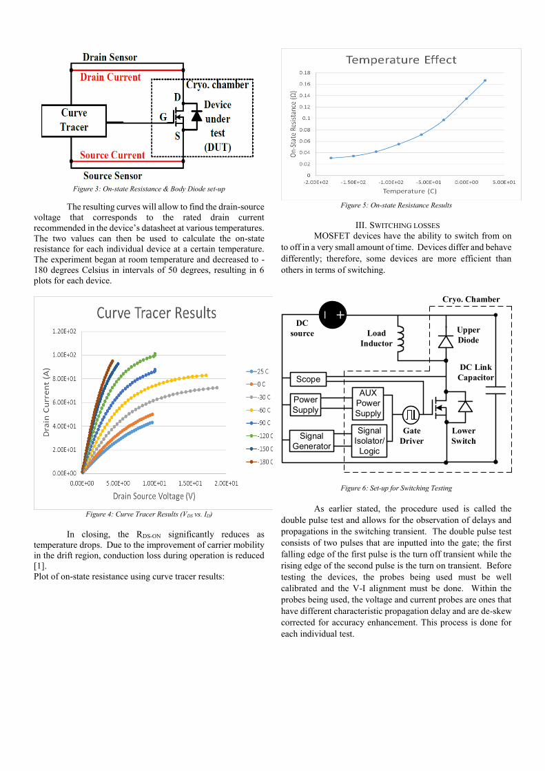
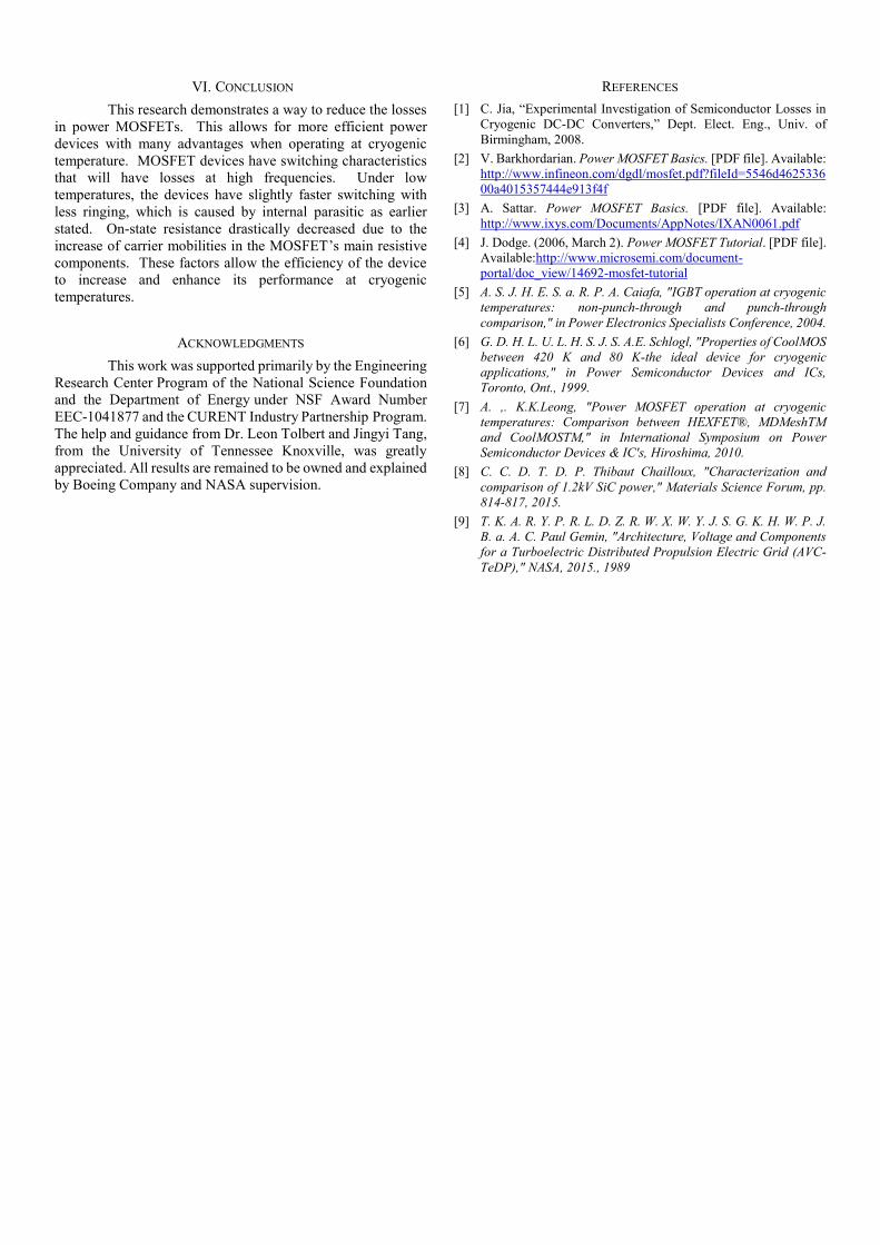
MOSFET Characteristics at Cryogenic Temperature Juan M. Avalos Electrical Engineering and Computer Science Department Christian Brothers University Memphis, TN USA [email protected]Leon Tolbert Electrical Engineering and Computer Science Department University of Tennessee Knoxville, TN USA [email protected]Abstract— Efficiency is a large concern in power electronics but size and weight must be taken into consideration as well. Power devices in need of thermal sinks for appropriate performance will affect both size and weight. MOSFET devices are the main components in the power electronics world because of their comparatively promising characteristics in power loss and switching performance. The objective of this research is to obtain results as to how the MOSFET device will perform in various temperatures that go as low as liquid nitrogen temperatures. More than one device was tested and compared in order to get the best performing. It is believed Cryogenic operation of MOSFET devices results in improved performance and efficiency. The switching performance of the devices will be analyzed using the Double Pulse Test (DPT). Ultimately, the objective of this research is to design a DC-AC inverter for Boeing & NASA aircraft using the best performing MOSFET device. Index Terms—Double Pulse Test, Power Inverter, Cryogenic Temperature I. INTRODUCTION It is essential to understand the structure of MOSFET devices and the Double Pulse Test process that is used to analyze them. There are four main characteristics that are being observed for each device. Each defines the device’s efficiency and performance. On-state resistance, switching loss, body diode, and breakdown voltage are the four characteristics that will be affected by the change in temperature and determine the device performance gains. Different techniques are used to obtain each one and will be discussed further on. The purpose of the Double Pulse Test is to obtain data reflecting the switching characterization of power devices in a simplified printed circuit board (PCB). This board allows to evaluate their switching behaviors as if in an actual power converter. The Double Pulse Test consists of manually triggering two pulse as an input to the gate of the device. Each pulse has its purpose and effect to the device. The length of the first pulse, in time, builds up a desired current through the inductor load. The switching transient consists of the turn off and turn on of the device. The falling edge of the first pulse corresponds to the turn off transient while the rising edge of the second pulse corresponds to the turn off. The components required for this set up are the following: Device Under Test (DUT) Inductive Load Auxiliary DC Power Supply Waveform Generator DC bus Gate drive/driver board Oscilloscope Lab procedures for testing devices have to be taken into consideration for accurate results. Initially, probe compensation and de-skew correction are necessary for voltage-current alignment. The yellow scope must compensate for the input at the gate of the MOSFET while the blue scope compensates for the drain source voltage. As it is usually assumed, the channel 1 with yellow waveforms is used as gate- source voltage measurement, the channel 2 with blue waveforms is used as drain-source voltage measurement, the channel 3 with purple waveforms is used as drain-current measurement, and the channel 4 with green waveforms is used as load-current measurement. The purple current probe is de- skewed and the propagation delay for all are minimized as much as possible. The probes have different purposes such as the probes being used in channels 1 and 2 for voltage measurement. The difference in those two channels are the voltage levels: 1 for ≤ 600V; 2 for 600V ~ 1200V. Different probes will have different parasitic, which will cause the error of the measurement, in order to avoid that, the de-skew process was conducted. Meanwhile, when the 600V-level test was conducted, same type of probes was used for both channel 1 and 2, the de-skew process was not necessary in this case. Before any testing is done to the devices, the circuit board must have exposed, conductive parts covered. Icing at lower temperatures can cause problems such as shorts in the circuit leading to damaging equipment. The lowest temperature, for the chamber, allowed is 93 K (-180°C) and the highest temperature tested is 23 K (room temperature). Once the board is ready, it is placed inside the chamber even for room temperature testing. The room temperature testing is done after the chamber has been heated up for moisture dissipation. This procedure mitigates humidity in the inner chamber and reduces the possibility of short-circuiting due to icing at cryogenic temperature.
Transcript
MOSFET Characteristics at Cryogenic Temperature
Juan M. Avalos Electrical Engineering and Computer Science Department