National Aeronautics and Space Administration MRAM Technology Status Jason Heidecker Jet Propulsion Laboratory Pasadena, California Jet Propulsion Laboratory California Institute of Technology Pasadena, California JPL Publication 13-3 2/13
Transcript
National Aeronautics and Space Administration
MRAM Technology Status
Jason Heidecker Jet Propulsion Laboratory
Pasadena, California
Jet Propulsion Laboratory California Institute of Technology
Pasadena, California
JPL Publication 13-3 2/13
i
National Aeronautics and Space Administration
MRAM Technology Status
NASA Electronic Parts and Packaging (NEPP) Program Office of Safety and Mission Assurance
Jason Heidecker Jet Propulsion Laboratory
Pasadena, California
NASA WBS: 104593 JPL Project Number: 104593 Task Number: 40.49.01.09
Jet Propulsion Laboratory 4800 Oak Grove Drive Pasadena, CA 91109
http://nepp.nasa.gov
ii
This research was carried out at the Jet Propulsion Laboratory, California Institute of Technology, and was
sponsored by the National Aeronautics and Space Administration Electronic Parts and Packaging (NEPP) Program.
Reference herein to any specific commercial product, process, or service by trade name, trademark, manufacturer, or
otherwise, does not constitute or imply its endorsement by the United States Government or the Jet Propulsion
5.0 Comparison to Other NVM .................................................................................................................................. 22
6.0 Flight Heritage ..................................................................................................................................................... 23 6.1 TAMU Onboard Sprite-Sat; January 2009 Launch ..................................................................................... 23 6.2 COVE Onboard M-Cubed; October 2011 Launch ...................................................................................... 23 6.3 Honeywell and Aeroflex Space MRAM ....................................................................................................... 24
1.0 INTRODUCTION Magnetoresistive Random Access Memory (MRAM) is different from conventional types of memory like SRAM, DRAM, and Flash, where electric charge is used to store information. Instead of exploiting the charge of an electron, MRAM uses its spin to store data. This type of electronics is known as “spintronics.”
At the heart of MRAM’s spintronic nature is the magnetic tunnel junction (MTJ), a thin-film structure comprised of many ferromagnetic and nonmagnetic layers. The resistance of the MTJ, and therefore bit state of the memory element, switches purely with the change in polarization of these layers. Since these materials can hold their polarization virtually forever when unpowered, MRAM therefore falls into the nonvolatile memory (NVM) camp, along with Flash, FeRAM, and EEPROM.
To system designers in the 1960s and 70s, when semiconductor memories where relatively new, the standard way of thinking was “look to volatile memories when speed and density are important but power is not” and “look to nonvolatile memories when power is important but density and speed are not.” These were simple rules that held true for the technologies available at the time like DRAM, SRAM, and EEPROM. However, today’s memory landscape includes so many technologies that making such a strict distinction is no longer possible. Each type of memory has a unique set of advantages and disadvantages, and there are “ideal memory” candidates that promise to combine the strengths of many technologies without the weaknesses. One such candidate is the next generation of MRAM, based on spin-torque technology, known as ST-MRAM. It promises to combine the nonvolatility of Flash, the density of DRAM, the speed of SRAM, and radiation-hardness of MRAM.
However, ST-MRAM only recently went into production, so it will be many more years before it has the track record and demonstrated reliability to be considered for space application. Therefore ST-MRAM is only briefly discussed in this report. The current MRAM technology, known as toggle MRAM, will be the technology of choice for space systems in the coming years. This report focuses on toggle MRAM and its technology, reliability, vendors, and space-readiness.
2
2.0 MRAM TECHNOLOGY
2.1 Magnetic Core Memory, the First “MRAM” Magnetic memories were first introduced in the 1950s. These were not labeled “MRAMs” but were instead known as “magnetic core memories” and were the predominant form of RAM until the mid-70s (Figure 2.1-1). They used ferrite toroids (rings/cores) arranged in an x–y grid configuration. Four wires were threaded through each ferrite core: X/Y/sense/inhibit. These were used to select bits, change their state, and read them out. Each core represented one bit of information. A magnetic field was used to sense the memory element, and the polarity of induced voltages in a sensing circuit depended on whether a “1” or “0” was stored.
Figure 2.1-1. Magnetic core memory used in the 1950s, the first magnetic memory.
The memory shown here stored 32×32 (1024) bits of data [1].
2.2 Magnetoresistance, Thin-Film MRAM It was not until the 1980s that the first MRAMs based on thin-film ferromagnetic materials were introduced [2]. These early MRAMs were based on the fact that the resistance of a ferromagnetic conductor depended on the angle between the applied current and the magnetic polarization of the conductor, a phenomenon called anisotropic magnetoresistance (AMR). Technologies built on AMR were the first “spintronics,” as they were the first to exploit both the charge and spin of an electron. These original AMR MRAMs were developed by companies like Honeywell, NonVolatile Electronics, Inc. (NVE), and Iowa State University. In contrast to the magnetic core memories of the 1950s and 60s that were basically mechanical apparatuses, these thin-film MRAMs were actual integrated circuits made with modern photolithographic processes with CMOS control circuitry.
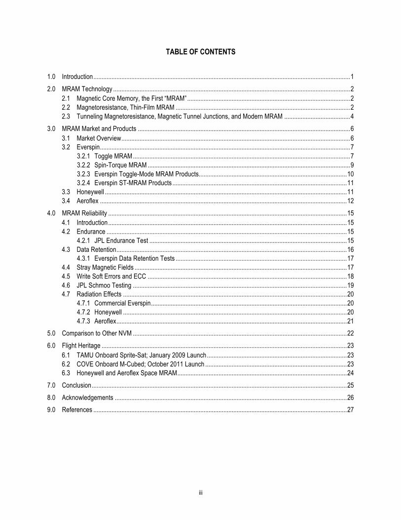
The Corbino disc in Figure 2.2-1 illustrates the AMR phenomenon that made the first MRAMs possible. It is called “anisotropic” because it is directionally dependent (the effect is strongest when B field and current are perpendicular, and zero when they are parallel, according to the classic right-hand rule). The disc has an inner and outer electrode separated by ferromagnetic material. When a voltage is applied, the ferromagnetic material provides a resistance and the resulting current is Iρ. When a perpendicular magnetic field is applied to the disc, a magnetic force is exerted on the moving charges, thereby adding current component Iθ. This acts to restrict the flow of Iρ, thereby increasing the resistance of the disc.
3
Figure 2.2-1. The Corbino disc.
Resistance from inner electrode to outer electrode varies with applied B field [3].
The AMR effect could only provide changes in resistance on the order of 2%, which is not sufficient for commercial MRAMs. The largest device built by Honeywell was only 16 kb [4]. However, the technology did find its way into hard disk read heads, which hard disks still use today.
When researchers began to experiment with multilayer structures in the late 1980s, much higher changes in resistance (50% instead of 2%) were observed [5]. This phenomenon was called giant magnetoresistance (GMR) and AMR technologies were quickly abandoned for use in memories (AMR is still the technology used in hard disk read heads). The 2007 Nobel Prize in Physics was awarded to both Albert Fert of the U.S. and Peter Grunberg of Germany for their independent efforts in the 1980s that led to the discovery of GMR.
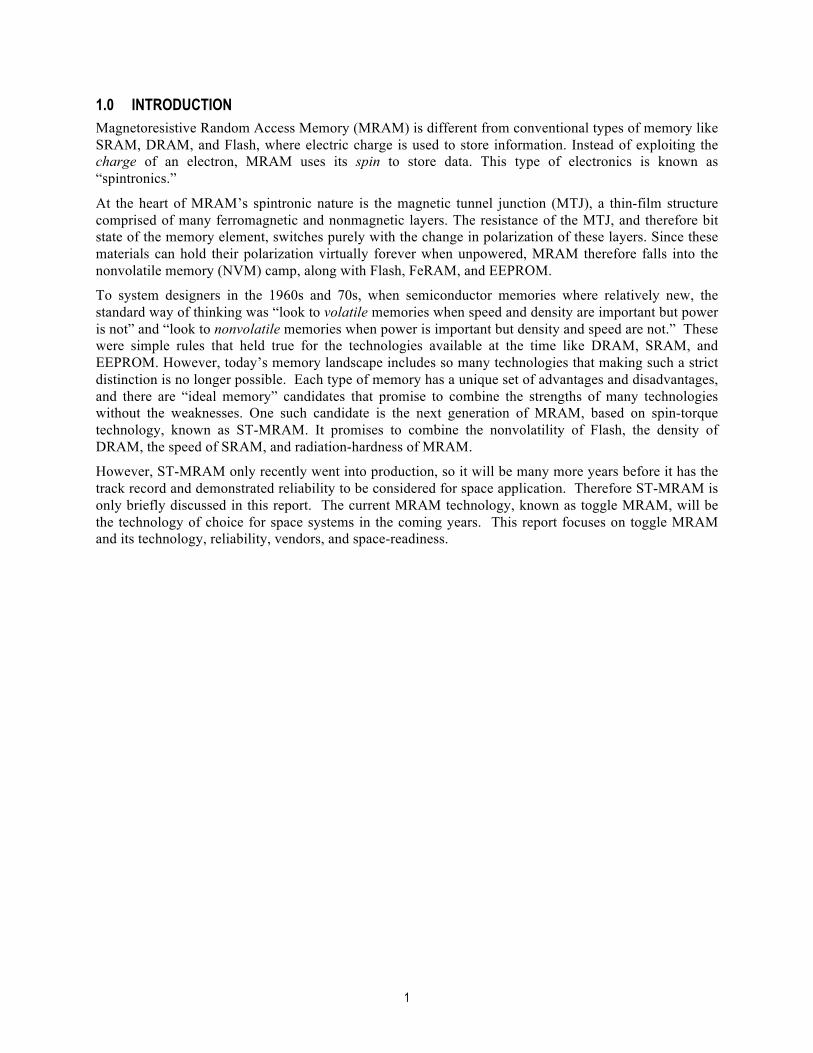
GMR was seen in thin-film structures, composed of alternating ferromagnetic and nonmagnetic layers (e.g., Fe/Cr/Fe) (Figure 2.2-2). These are current-in-plane structures, where the current is measured going from left to right in Figure 2.2-2, not from top to bottom. Resistance of the material is affected by aligning magnetic moments of the ferromagnetic layers, which creates changes in the scattering of spin-up or spin-down electrons. When the magnetizations of the two ferromagnetic layers are in parallel orientation, the electrical resistance is lower than when the magnetizations are antiparallel. Although changes of resistance as high as 50% have been seen in these structures, in practical memory cell application, only 4–8% is achieved.
Figure 2.2-2. GMR.
The free layer’s magnetic moment changes as it passes over magnetic material on the disc, thus changing the resistance of the structure and the current through it [6].
4
Providing even greater resistance than GMR is colossal magnetoresistance (CMR). This refers to very large changes in resistance under magnetic fields observed mostly in certain manganese oxide compounds. The effect was first discovered in the 1950s and still isn’t well understood to this day [7]. Due to its misunderstood nature and exotic material requirements, it has found little use in the memory market. Table 2.2-1 lists the various types of magnetoresistance and the increase in resistance that occurs.
Table 2.2-1. Types of magnetoresistance (MR).
Name Increase in Resistance Anisotropic (AMR) 2%
Giant (GMR) 25–50%
Tunnel (TMR) 50–70%
Colossal (CMR) 100+%
2.3 Tunneling Magnetoresistance, Magnetic Tunnel Junctions, and Modern MRAM Modern MRAMs are not based on AMR, GMR, or CMR, but instead tunnel magnetoresistance (TMR).
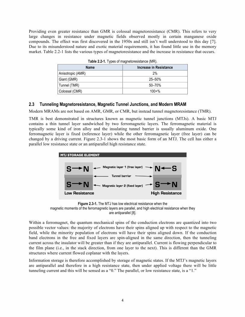
TMR is best demonstrated in structures known as magnetic tunnel junctions (MTJs). A basic MTJ contains a thin tunnel layer sandwiched by two ferromagnetic layers. The ferromagnetic material is typically some kind of iron alloy and the insulating tunnel barrier is usually aluminum oxide. One ferromagnetic layer is fixed (reference layer) while the other ferromagnetic layer (free layer) can be changed by a driving current. Figure 2.3-1 shows the most basic form of an MTJ. The cell has either a parallel low resistance state or an antiparallel high resistance state.
Figure 2.3-1. The MTJ has low electrical resistance when the
magnetic moments of the ferromagnetic layers are parallel, and high electrical resistance when they are antiparallel [8].
Within a ferromagnet, the quantum mechanical spins of the conduction electrons are quantized into two possible vector values: the majority of electrons have their spins aligned up with respect to the magnetic field, while the minority population of electrons will have their spins aligned down. If the conduction band electrons in the free and fixed layers are spin-aligned in the same direction, then the tunneling current across the insulator will be greater than if they are antiparallel. Current is flowing perpendicular to the film plane (i.e., in the stack direction, from one layer to the next). This is different than the GMR structures where current flowed coplanar with the layers.
Information storage is therefore accomplished by storage of magnetic states. If the MTJ’s magnetic layers are antiparallel and therefore in a high resistance state, then under applied voltage there will be little tunneling current and this will be sensed as a “0.” The parallel, or low resistance state, is a “1.”
5
During the 1970s and 80s, a variety of researchers experimented with thin-film structures consisting of ferromagnetic layers separated by a thin insulator of various materials. The change in resistance varied from 5 to 20%.
However, in the mid-1990s, several groups began working with iron alloys with aluminum oxide insulating barriers. This is how the current generation of MRAMs from Everspin is built, and their technology sees changes in resistance on the order of 40%. However, in the years since the Everspin products were designed, continued R&D with magnesium-based oxides by other institutions has seen increases in resistance as high as 1100% [9].
These more advanced structures exhibiting TMR could appear in future generations of MRAM. The higher resistance change means memory states are easier to sense, therefore current and power consumption decreases, further improving MRAM’s place in the memory market.
6
3.0 MRAM MARKET AND PRODUCTS
3.1 Market Overview To date, Everspin is the only company to have successfully commercialized MRAM. Many other companies have had R&D efforts (some still do) but never commercialized a product: IBM, Infineon, Toshiba, Samsung, Micron, Sony, Hitachi, NVE, Intel, Cypress, NEC, Crocus, Spintec, Spin Transfer Technologies, Fujitsu, and Grandis, to name a few. It is the opinion of the author that these companies are waiting for second-generation MRAM based on spin-torque (ST) technology to mature further before working on their own products, as ST promises much higher densities and performance (and therefore has greater market potential). Most of the R&D money spent by these companies is on ST. Also, as discussed further below, the MRAM market to date has only supported less than 10 million total units sold, which is too small to attract the likes of IBM, Toshiba, Samsung, or Micron.
Everspin started out as Motorola in the 1990s, which developed their patented 10-layer MTJ bit element structure and toggle program method. First-generation MRAM devices in production today are known as toggle MRAMs, after this program method. (ST-MRAMs, as discussed in more detail below, have a much simpler program method.) In 2004, Motorola spun off Freescale, who produced the first 4 Mb MRAM in 2006. Then, in 2008, Freescale spun off Everspin.
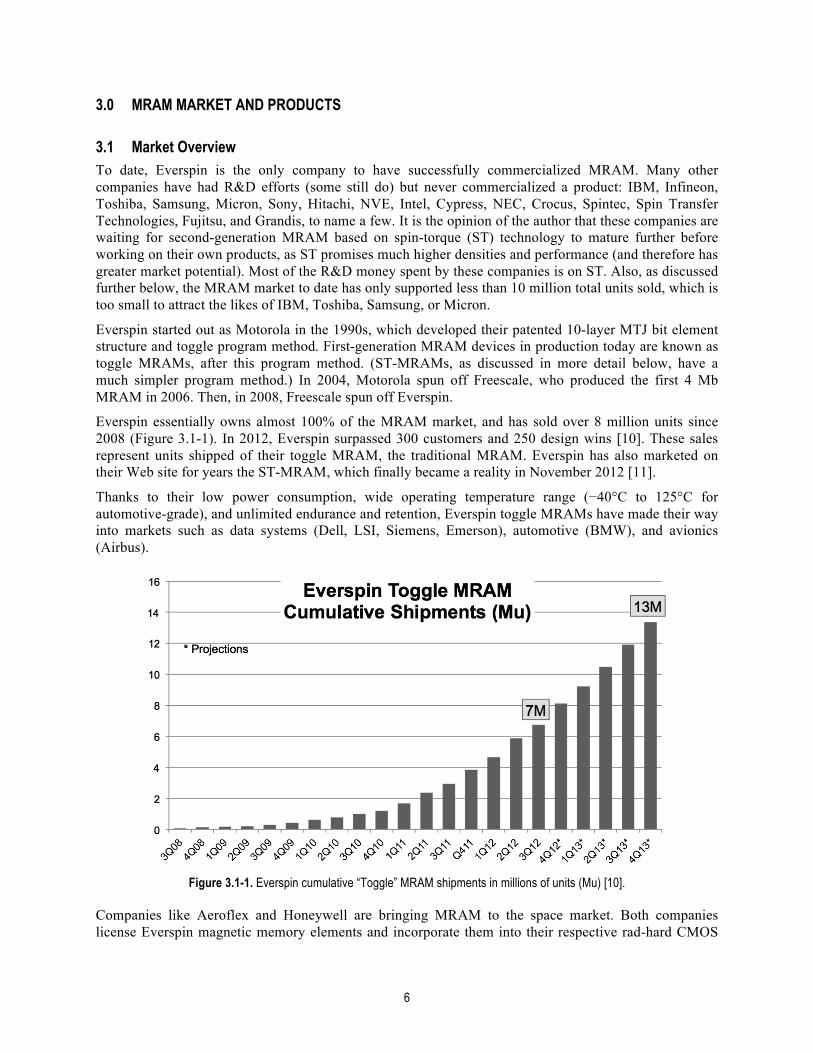
Everspin essentially owns almost 100% of the MRAM market, and has sold over 8 million units since 2008 (Figure 3.1-1). In 2012, Everspin surpassed 300 customers and 250 design wins [10]. These sales represent units shipped of their toggle MRAM, the traditional MRAM. Everspin has also marketed on their Web site for years the ST-MRAM, which finally became a reality in November 2012 [11].
Thanks to their low power consumption, wide operating temperature range (−40°C to 125°C for automotive-grade), and unlimited endurance and retention, Everspin toggle MRAMs have made their way into markets such as data systems (Dell, LSI, Siemens, Emerson), automotive (BMW), and avionics (Airbus).
Figure 3.1-1. Everspin cumulative “Toggle” MRAM shipments in millions of units (Mu) [10].
Companies like Aeroflex and Honeywell are bringing MRAM to the space market. Both companies license Everspin magnetic memory elements and incorporate them into their respective rad-hard CMOS
7
processes. These products are currently undergoing qualification by the Defense Logistics Agency (DLA) in order to be listed on the QPL for fast-track acceptance into space programs.
These products are discussed later in this report, including technology, qualification status, and product roadmap. First, the underlying commercial Everspin technology is covered.
3.2 Everspin The only commercial MRAM on the market today is from Everspin. Everspin’s first commercial MRAM was released in 2004 when the company was still Freescale. It was a 35-ns, read-cycle device manufactured on 180-nm CMOS, with a density of 4 Mb. Eight years later, they have only advanced this toggle MRAM to 16 Mb devices made on 130-nm CMOS. The CMOS and magnetics are all fabricated on the same line at the Everspin facility in Chandler, Arizona.
Everspin is also the developer of second-generation spin-torque MRAM, which uses the same MTJ structure in toggle MRAM, but has a much simpler program method, making the overall memory array structure much simpler, lending itself to much greater densities than toggle MRAM. Another major difference between toggle and ST-MRAM is that the former is SRAM or SPI-based, while the later has a DRAM-like architecture. ST-MRAM promises to leap MRAM ahead a few generations in terms of density and performance.
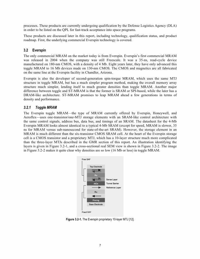
3.2.1 Toggle MRAM The Everspin toggle MRAM—the type of MRAM currently offered by Everspin, Honeywell, and Aeroflex—uses one-transistor/one-MTJ storage elements with an SRAM-like control architecture with the same control signals, address bus, data bus, and timings of an SRAM. The datasheet for the 4-Mb Everspin MRAM looks almost identical to a typical 4-Mb SRAM (except for speed, MRAM is slower, 35 ns for MRAM versus sub-nanosecond for state-of-the-art SRAM). However, the storage element in an MRAM is much different than the six-transistor CMOS SRAM cell. At the heart of the Everspin storage cell is a CMOS transistor and a proprietary MTJ, which has a 10-layer structure much more complicated than the three-layer MTJs described in the GMR section of this report. An illustration identifying the layers is given in Figure 3.2-1, and a cross-sectional real SEM view is shown in Figure 3.2-2. The image in Figure 3.2-2 makes it quite clear why densities are so low (16 Mb or less) in toggle MRAM.
Figure 3.2-1. The Everspin proprietary 10-layer MTJ [12].
8
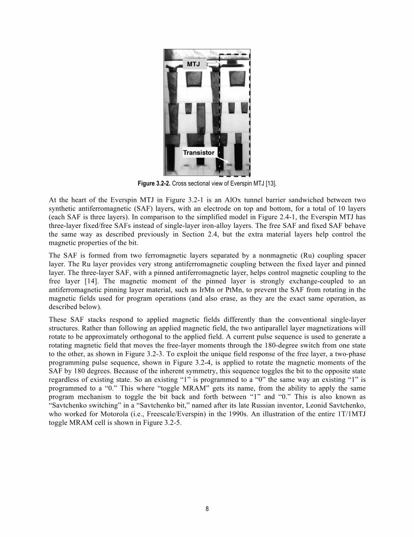
Figure 3.2-2. Cross sectional view of Everspin MTJ [13].
At the heart of the Everspin MTJ in Figure 3.2-1 is an AlOx tunnel barrier sandwiched between two synthetic antiferromagnetic (SAF) layers, with an electrode on top and bottom, for a total of 10 layers (each SAF is three layers). In comparison to the simplified model in Figure 2.4-1, the Everspin MTJ has three-layer fixed/free SAFs instead of single-layer iron-alloy layers. The free SAF and fixed SAF behave the same way as described previously in Section 2.4, but the extra material layers help control the magnetic properties of the bit.
The SAF is formed from two ferromagnetic layers separated by a nonmagnetic (Ru) coupling spacer layer. The Ru layer provides very strong antiferromagnetic coupling between the fixed layer and pinned layer. The three-layer SAF, with a pinned antiferromagnetic layer, helps control magnetic coupling to the free layer [14]. The magnetic moment of the pinned layer is strongly exchange-coupled to an antiferromagnetic pinning layer material, such as IrMn or PtMn, to prevent the SAF from rotating in the magnetic fields used for program operations (and also erase, as they are the exact same operation, as described below).
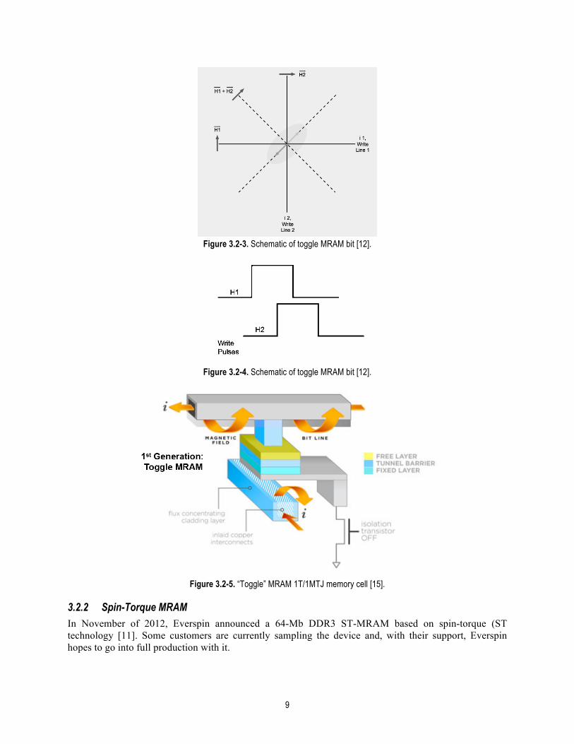
These SAF stacks respond to applied magnetic fields differently than the conventional single-layer structures. Rather than following an applied magnetic field, the two antiparallel layer magnetizations will rotate to be approximately orthogonal to the applied field. A current pulse sequence is used to generate a rotating magnetic field that moves the free-layer moments through the 180-degree switch from one state to the other, as shown in Figure 3.2-3. To exploit the unique field response of the free layer, a two-phase programming pulse sequence, shown in Figure 3.2-4, is applied to rotate the magnetic moments of the SAF by 180 degrees. Because of the inherent symmetry, this sequence toggles the bit to the opposite state regardless of existing state. So an existing “1” is programmed to a “0” the same way an existing “1” is programmed to a “0.” This where “toggle MRAM” gets its name, from the ability to apply the same program mechanism to toggle the bit back and forth between “1” and “0.” This is also known as “Savtchenko switching” in a “Savtchenko bit,” named after its late Russian inventor, Leonid Savtchenko, who worked for Motorola (i.e., Freescale/Everspin) in the 1990s. An illustration of the entire 1T/1MTJ toggle MRAM cell is shown in Figure 3.2-5.
3.2.2 Spin-Torque MRAM In November of 2012, Everspin announced a 64-Mb DDR3 ST-MRAM based on spin-torque (ST technology [11]. Some customers are currently sampling the device and, with their support, Everspin hopes to go into full production with it.
10
The ST-MRAM has a DDR3 SDRAM-like architecture instead of the SRAM-like architecture that the toggle MRAM has. It is compliant to the industry standard JEDEC DDR3 specification. This means 3.2 GBytes/second with nanosecond-class latency. One thing missing from the MRAM datasheet, which is a significant advantage over DRAM, is a refresh requirement due to MRAM’s nonvolatility. The target application for these devices is SSD storage and RAID systems where a fast, nonvolatile memory is needed as data buffers and cache memories.
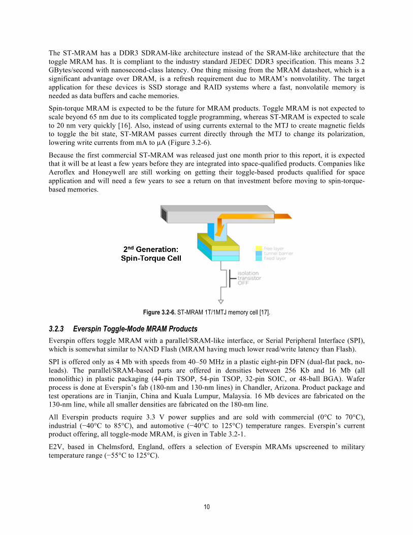
Spin-torque MRAM is expected to be the future for MRAM products. Toggle MRAM is not expected to scale beyond 65 nm due to its complicated toggle programming, whereas ST-MRAM is expected to scale to 20 nm very quickly [16]. Also, instead of using currents external to the MTJ to create magnetic fields to toggle the bit state, ST-MRAM passes current directly through the MTJ to change its polarization, lowering write currents from mA to µA (Figure 3.2-6).
Because the first commercial ST-MRAM was released just one month prior to this report, it is expected that it will be at least a few years before they are integrated into space-qualified products. Companies like Aeroflex and Honeywell are still working on getting their toggle-based products qualified for space application and will need a few years to see a return on that investment before moving to spin-torque-based memories.
Figure 3.2-6. ST-MRAM 1T/1MTJ memory cell [17].
3.2.3 Everspin Toggle-Mode MRAM Products Everspin offers toggle MRAM with a parallel/SRAM-like interface, or Serial Peripheral Interface (SPI), which is somewhat similar to NAND Flash (MRAM having much lower read/write latency than Flash).
SPI is offered only as 4 Mb with speeds from 40–50 MHz in a plastic eight-pin DFN (dual-flat pack, no-leads). The parallel/SRAM-based parts are offered in densities between 256 Kb and 16 Mb (all monolithic) in plastic packaging (44-pin TSOP, 54-pin TSOP, 32-pin SOIC, or 48-ball BGA). Wafer process is done at Everspin’s fab (180-nm and 130-nm lines) in Chandler, Arizona. Product package and test operations are in Tianjin, China and Kuala Lumpur, Malaysia. 16 Mb devices are fabricated on the 130-nm line, while all smaller densities are fabricated on the 180-nm line.
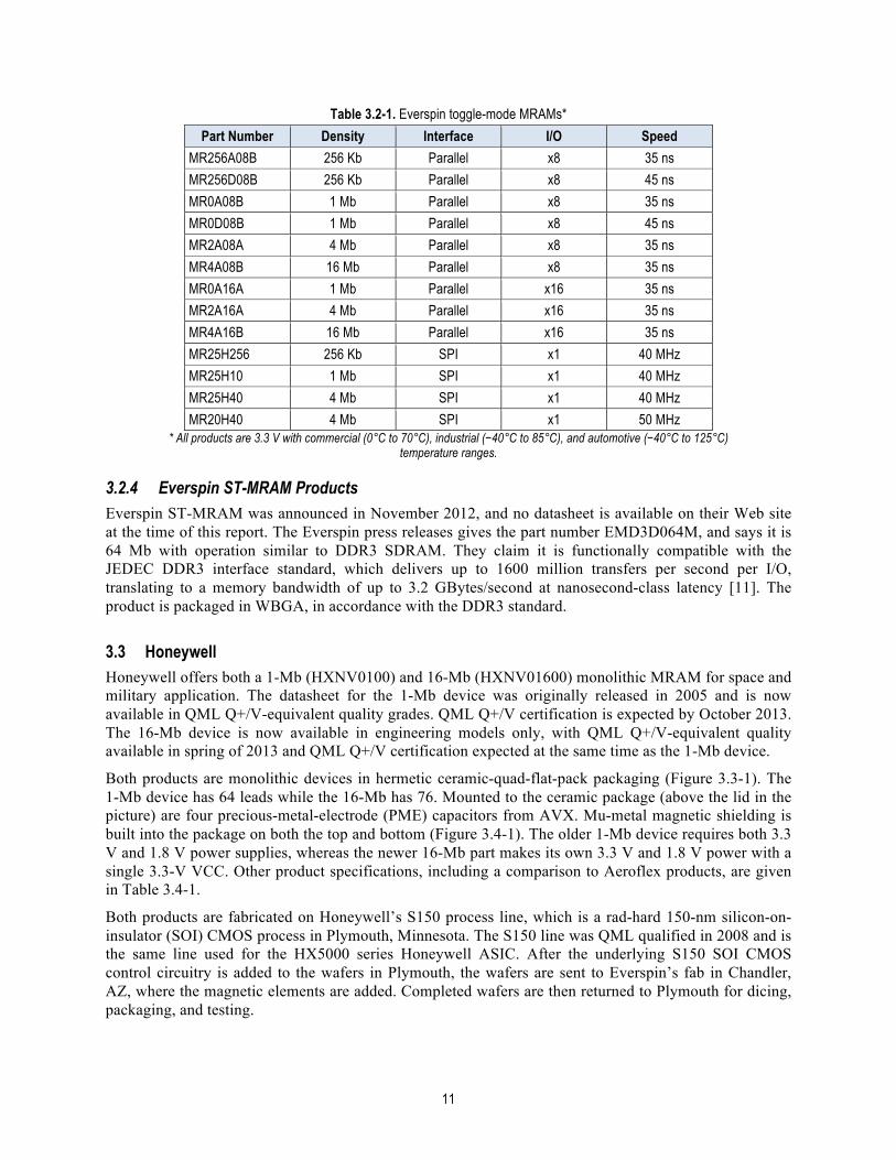
All Everspin products require 3.3 V power supplies and are sold with commercial (0°C to 70°C), industrial (−40°C to 85°C), and automotive (−40°C to 125°C) temperature ranges. Everspin’s current product offering, all toggle-mode MRAM, is given in Table 3.2-1.
E2V, based in Chelmsford, England, offers a selection of Everspin MRAMs upscreened to military temperature range (−55°C to 125°C).
11
Table 3.2-1. Everspin toggle-mode MRAMs*
Part Number Density Interface I/O Speed MR256A08B 256 Kb Parallel x8 35 ns
MR256D08B 256 Kb Parallel x8 45 ns
MR0A08B 1 Mb Parallel x8 35 ns
MR0D08B 1 Mb Parallel x8 45 ns
MR2A08A 4 Mb Parallel x8 35 ns
MR4A08B 16 Mb Parallel x8 35 ns
MR0A16A 1 Mb Parallel x16 35 ns
MR2A16A 4 Mb Parallel x16 35 ns
MR4A16B 16 Mb Parallel x16 35 ns
MR25H256 256 Kb SPI x1 40 MHz
MR25H10 1 Mb SPI x1 40 MHz
MR25H40 4 Mb SPI x1 40 MHz
MR20H40 4 Mb SPI x1 50 MHz * All products are 3.3 V with commercial (0°C to 70°C), industrial (−40°C to 85°C), and automotive (−40°C to 125°C)
temperature ranges.
3.2.4 Everspin ST-MRAM Products Everspin ST-MRAM was announced in November 2012, and no datasheet is available on their Web site at the time of this report. The Everspin press releases gives the part number EMD3D064M, and says it is 64 Mb with operation similar to DDR3 SDRAM. They claim it is functionally compatible with the JEDEC DDR3 interface standard, which delivers up to 1600 million transfers per second per I/O, translating to a memory bandwidth of up to 3.2 GBytes/second at nanosecond-class latency [11]. The product is packaged in WBGA, in accordance with the DDR3 standard.
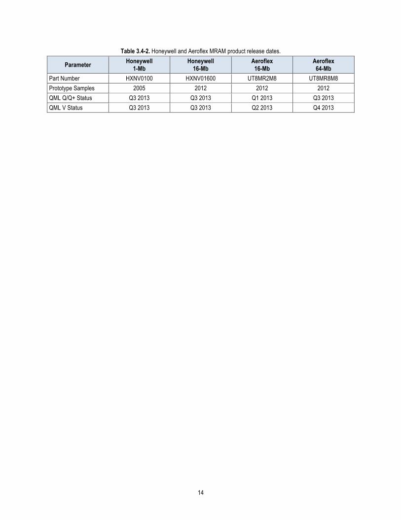
3.3 Honeywell Honeywell offers both a 1-Mb (HXNV0100) and 16-Mb (HXNV01600) monolithic MRAM for space and military application. The datasheet for the 1-Mb device was originally released in 2005 and is now available in QML Q+/V-equivalent quality grades. QML Q+/V certification is expected by October 2013. The 16-Mb device is now available in engineering models only, with QML Q+/V-equivalent quality available in spring of 2013 and QML Q+/V certification expected at the same time as the 1-Mb device.
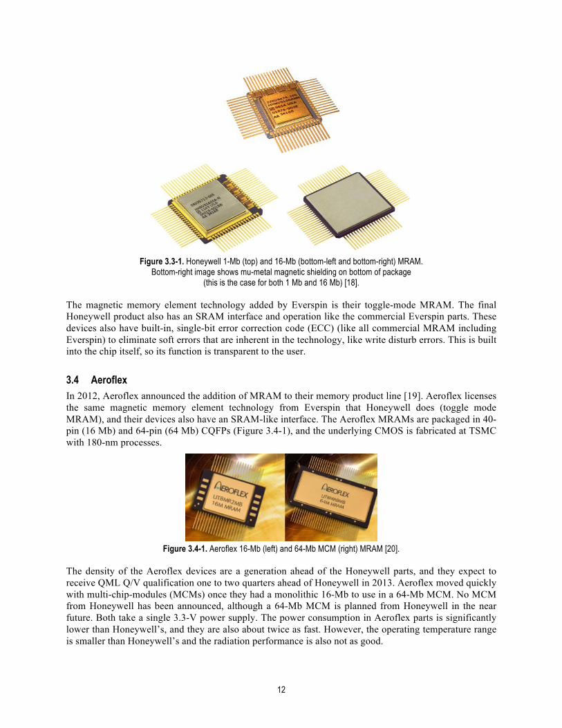
Both products are monolithic devices in hermetic ceramic-quad-flat-pack packaging (Figure 3.3-1). The 1-Mb device has 64 leads while the 16-Mb has 76. Mounted to the ceramic package (above the lid in the picture) are four precious-metal-electrode (PME) capacitors from AVX. Mu-metal magnetic shielding is built into the package on both the top and bottom (Figure 3.4-1). The older 1-Mb device requires both 3.3 V and 1.8 V power supplies, whereas the newer 16-Mb part makes its own 3.3 V and 1.8 V power with a single 3.3-V VCC. Other product specifications, including a comparison to Aeroflex products, are given in Table 3.4-1.
Both products are fabricated on Honeywell’s S150 process line, which is a rad-hard 150-nm silicon-on-insulator (SOI) CMOS process in Plymouth, Minnesota. The S150 line was QML qualified in 2008 and is the same line used for the HX5000 series Honeywell ASIC. After the underlying S150 SOI CMOS control circuitry is added to the wafers in Plymouth, the wafers are sent to Everspin’s fab in Chandler, AZ, where the magnetic elements are added. Completed wafers are then returned to Plymouth for dicing, packaging, and testing.
12
Figure 3.3-1. Honeywell 1-Mb (top) and 16-Mb (bottom-left and bottom-right) MRAM.
Bottom-right image shows mu-metal magnetic shielding on bottom of package (this is the case for both 1 Mb and 16 Mb) [18].
The magnetic memory element technology added by Everspin is their toggle-mode MRAM. The final Honeywell product also has an SRAM interface and operation like the commercial Everspin parts. These devices also have built-in, single-bit error correction code (ECC) (like all commercial MRAM including Everspin) to eliminate soft errors that are inherent in the technology, like write disturb errors. This is built into the chip itself, so its function is transparent to the user.
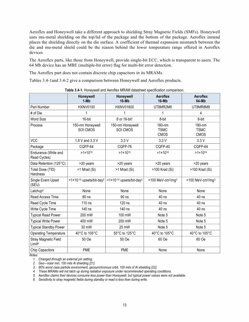
3.4 Aeroflex In 2012, Aeroflex announced the addition of MRAM to their memory product line [19]. Aeroflex licenses the same magnetic memory element technology from Everspin that Honeywell does (toggle mode MRAM), and their devices also have an SRAM-like interface. The Aeroflex MRAMs are packaged in 40-pin (16 Mb) and 64-pin (64 Mb) CQFPs (Figure 3.4-1), and the underlying CMOS is fabricated at TSMC with 180-nm processes.
The density of the Aeroflex devices are a generation ahead of the Honeywell parts, and they expect to receive QML Q/V qualification one to two quarters ahead of Honeywell in 2013. Aeroflex moved quickly with multi-chip-modules (MCMs) once they had a monolithic 16-Mb to use in a 64-Mb MCM. No MCM from Honeywell has been announced, although a 64-Mb MCM is planned from Honeywell in the near future. Both take a single 3.3-V power supply. The power consumption in Aeroflex parts is significantly lower than Honeywell’s, and they are also about twice as fast. However, the operating temperature range is smaller than Honeywell’s and the radiation performance is also not as good.
13
Aeroflex and Honeywell take a different approach to shielding Stray Magnetic Fields (SMFs). Honeywell uses mu-metal shielding on the top/lid of the package and the bottom of the package. Aeroflex instead places the shielding directly on the die surface. A coefficient of thermal expansion mismatch between the die and mu-metal shield could be the reason behind the lower temperature range offered in Aeroflex devices
The Aeroflex parts, like those from Honeywell, provide single-bit ECC, which is transparent to users. The 64 Mb device has an MBE (multiple-bit error) flag for multi-bit error detection.
The Aeroflex part does not contain discrete chip capacitors in its MRAMs.
Tables 3.4-1and 3.4-2 give a comparison between Honeywell and Aeroflex products.
Table 3.4-1. Honeywell and Aeroflex MRAM datasheet specification comparison.
Honeywell 1-Mb
Honeywell 16-Mb
Aeroflex 16-Mb
Aeroflex 64-Mb
Part Number HXNV0100 HXNV01600 UT8MR2M8 UT8MR8M8
# of Die 1 1 1 4
Word Size 16-bit 8 or 16-bit1 8-bit 8-bit
Process 150-nm Honeywell SOI CMOS
150-nm Honeywell SOI CMOS
180-nm TSMC CMOS
180-nm TSMC CMOS
VCC 1.8 V and 3.3 V 3.3 V 3.3 V 3.3 V
Package CQFP-64 CQFP-76 CQFP-40 CQFP-64
Endurance (Write and Read Cycles)
>1×10¹⁵ >1×10¹⁵ >1×10¹⁴ >1×10¹⁴
Data Retention (125°C) >20 years >20 years >20 years >20 years
Operating Temperature 40°C to 105°C 55°C to 125°C 40°C to 105°C 40°C to 105°C
Stray Magnetic Field Limit6
50 Oe 50 Oe 60 Oe 60 Oe
Chip Capacitors PME PME None None Notes:
1. Changed through an external pin setting. 2. Geo—solar min, 100 mils Al shielding [21]. 3. 90% worst case particle environment, geosynchronous orbit, 100 mils of Al shielding [22]. 4. These MRAMs will not latch up during radiation exposure under recommended operating conditions. 5. Aeroflex claims their devices consume less power than Honeywell, but typical power values were not available. 6. Sensitivity to stray magnetic fields during standby or read is less than during write.
14
Table 3.4-2. Honeywell and Aeroflex MRAM product release dates.
Parameter Honeywell 1-Mb
Honeywell 16-Mb
Aeroflex 16-Mb
Aeroflex 64-Mb
Part Number HXNV0100 HXNV01600 UT8MR2M8 UT8MR8M8
Prototype Samples 2005 2012 2012 2012
QML Q/Q+ Status Q3 2013 Q3 2013 Q1 2013 Q3 2013
QML V Status Q3 2013 Q3 2013 Q2 2013 Q4 2013
15
4.0 MRAM RELIABILITY
4.1 Introduction MRAM reliability, like the reliability of any other integrated circuit, is a topic that contains a number of focus areas including data integrity issues related to the MTJ memory bit itself, packaging related issues, CMOS reliability, and data integrity issues related to the memory array’s architecture and operation.
However, reliability in all of these areas has been covered very well by MRAM vendors such as Everspin (MTJ related risks) and Honeywell/Aeroflex (packaging and CMOS related risks). This report will focus on endurance, data retention, temperature, and voltage performance.
4.2 Endurance MTJ-based MRAM has virtually unlimited program/erase/read endurance, meaning you can write/read/erase the memory array virtually forever without degrading the MTJ’s ability to change or maintain its bit state. Toggling the magnetic moment of the free SAF layer to change bit state is a nondestructive process as charge transport does not occur, except for a small tunnel current across the AlOx barrier. MRAM datasheets typically quote about 1015 cycles for their endurance specification. This is effectively unlimited endurance as it takes over 300 years to write just 100,000 addresses even 1012 times (assuming 100 ns write-cycle time).
MRAMs are expected to have very high endurance and testing to date has demonstrated this. One of the largest customers of MRAM is Siemens. Siemens uses Everspin MRAM in over 250,000 systems and has reported zero field failures [10].
4.2.1 JPL Endurance Test An endurance test was performed at JPL on commercial Everspin parts, which use the same MTJs and toggle-mode operation as Honeywell and Aeroflex devices.
The device under test (DUT) was Everspin MR4A16BCYS35, a 3.3 V device organized as 1,048,576 words of 16 bits, and is specified to operate from −40°C to +95°C with an unlimited read/write endurance. The device has built-in, single-bit ECC.
Testing was performed using the JDI ATV digital tester. The layout and load board are shown in Figures 4.2-1 and 4.2-2.
Figures 4.2-1, 4.2-2. Layout design and picture of load board used for MRAM endurance test on JDI ATV.
16
Three samples were cycled at 25°C and no bit errors were observed during testing. The number of cycles performed per sample is given in Table 4.2-1. Cycling consisted of the following procedure, which would count as two cycles:
1. Write 0xAA 2. Read 0xAA (record addresses of any bit errors) 3. Write 0x55 4. Read 0x55 (record addresses of any bit errors).
Table 4.2-1. Everspin MR4A16B endurance test results.
Part Number SN 1 SN 2 SN 3 Total Number of Addresses Tested 100 100 100
Number of Cycles 1010 109 1010
Number of Bit Errors 0 0 0
4.3 Data Retention The failure mechanisms behind data retention in spintronics is different from traditional charge-storage-based memories. In floating-gate memories like NAND Flash, thermal excitation of the stored charge in the floating gate will cause it to leak off the gate, eventually changing the threshold voltage of the transistor enough to cause the wrong bit state (i.e., “1” instead of “0”) to be read out. This process is dependent on time and temperature, and independent of whether or not the device is powered (hence the term “nonvolatile”). In DRAM, a volatile memory, charge is stored in small capacitors, and the charge leaks out almost instantly when powered down, and on the order of 64 ms when powered on. However, with spin-based memories, the bit state changes not when charges leak, but when the polarization of the free magnetic layer or SAF in the MTJ flips, thus altering the resistance of the MTJ (refer back to Figure 2.4-1). In other words, in magnetic memory, magnetic polarization is stored rather than electrical charge.
Each of the two magnetic orientations for the free layer has an associated energy level. The energy levels of both orientations are equivalent, but there is an energy barrier to overcome when switching from one orientation to the other. The stability of a given magnetic state over time is intrinsically linked to the magnitude of the energy barrier between the two possible stable orientations of magnetization. The thermal disturbance of an individual bit can be equated to a randomly fluctuating magnetic field that acts to potentially disturb the magnetic state [23]. The magnitude of this equivalent random field is proportional to the device temperature. The effects of such random thermal fluctuations depend on the relative magnitudes of the energy barrier and the available thermal energy, which is proportional to the device temperature. If the energy barrier in a MTJ is comparable to the ambient thermal energy available to cause fluctuations, there is a good chance that the orientation can spontaneously flip from one orientation to the other in a random manner within the specified operating life of the device, thus creating a data storage error [23].
The thermal flip rate (TFR) can be modeled using a standard Arrhenius model for a two state system [24]:
𝑁 = 𝑁! 1 − 𝑒!!! ; 𝜏 = 𝜏!𝑒
! !!"
where N is the number of bit flips, N0 is the initial population of bits, τ0 where N is the number of bit flips, N0 is the initial population of bits, τ0 is the characteristic time at which the bit attempts to reverse from thermal fluctuations (~1 ns), E is the energy barrier separating the two stable states, and kT is the Boltzmann’s constant times the temperature. The ratio E/kT, also known as α, must be greater than approximately 70 at the highest operating temperature to ensure a TFR of less than 100 bits in 1 million 4-Mb parts over 10 years.
17
4.3.1 Everspin Data Retention Tests Akerman, et al., performed a data retention bake on 10 4-Mb parts [24]. Temperatures ranged from 120°C to 240°C and bake times ranged from two hours to three weeks. A checkerboard memory pattern was programmed prior to bake and read out afterwards. No bit errors were observed under any conditions. The most accelerated test consisted of 10 parts at 240°C for two hours, which would predict an α greater than 70 at 100°C and therefore give less than 100 ppm device fall out at 100°C.
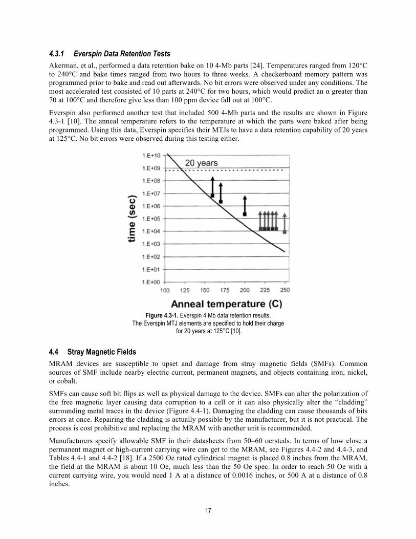
Everspin also performed another test that included 500 4-Mb parts and the results are shown in Figure 4.3-1 [10]. The anneal temperature refers to the temperature at which the parts were baked after being programmed. Using this data, Everspin specifies their MTJs to have a data retention capability of 20 years at 125°C. No bit errors were observed during this testing either.
Figure 4.3-1. Everspin 4 Mb data retention results.
The Everspin MTJ elements are specified to hold their charge for 20 years at 125°C [10].
4.4 Stray Magnetic Fields MRAM devices are susceptible to upset and damage from stray magnetic fields (SMFs). Common sources of SMF include nearby electric current, permanent magnets, and objects containing iron, nickel, or cobalt.
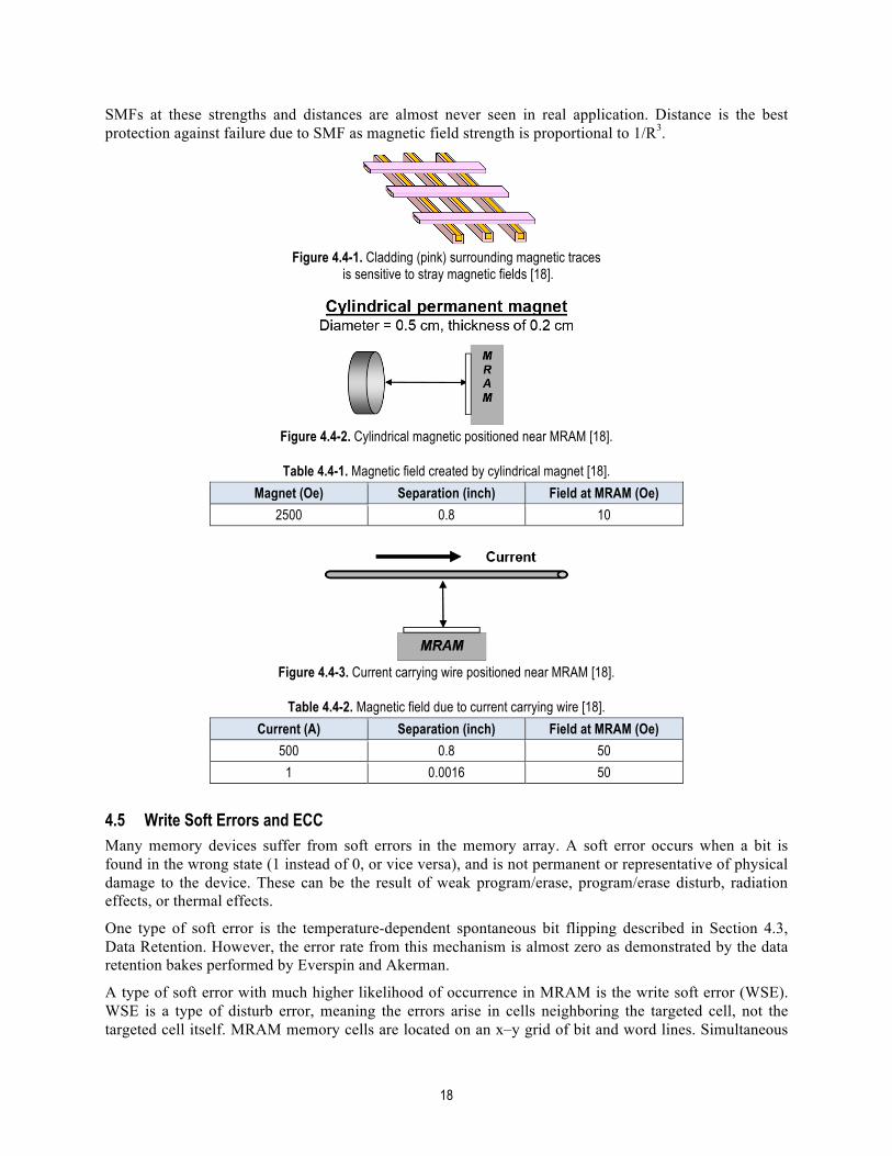
SMFs can cause soft bit flips as well as physical damage to the device. SMFs can alter the polarization of the free magnetic layer causing data corruption to a cell or it can also physically alter the “cladding” surrounding metal traces in the device (Figure 4.4-1). Damaging the cladding can cause thousands of bits errors at once. Repairing the cladding is actually possible by the manufacturer, but it is not practical. The process is cost prohibitive and replacing the MRAM with another unit is recommended.
Manufacturers specify allowable SMF in their datasheets from 50–60 oersteds. In terms of how close a permanent magnet or high-current carrying wire can get to the MRAM, see Figures 4.4-2 and 4.4-3, and Tables 4.4-1 and 4.4-2 [18]. If a 2500 Oe rated cylindrical magnet is placed 0.8 inches from the MRAM, the field at the MRAM is about 10 Oe, much less than the 50 Oe spec. In order to reach 50 Oe with a current carrying wire, you would need 1 A at a distance of 0.0016 inches, or 500 A at a distance of 0.8 inches.
18
SMFs at these strengths and distances are almost never seen in real application. Distance is the best protection against failure due to SMF as magnetic field strength is proportional to 1/R3.
Figure 4.4-1. Cladding (pink) surrounding magnetic traces
is sensitive to stray magnetic fields [18].
Figure 4.4-2. Cylindrical magnetic positioned near MRAM [18].
Table 4.4-1. Magnetic field created by cylindrical magnet [18].
Magnet (Oe) Separation (inch) Field at MRAM (Oe) 2500 0.8 10
Figure 4.4-3. Current carrying wire positioned near MRAM [18].
Table 4.4-2. Magnetic field due to current carrying wire [18].
Current (A) Separation (inch) Field at MRAM (Oe) 500 0.8 50
1 0.0016 50
4.5 Write Soft Errors and ECC Many memory devices suffer from soft errors in the memory array. A soft error occurs when a bit is found in the wrong state (1 instead of 0, or vice versa), and is not permanent or representative of physical damage to the device. These can be the result of weak program/erase, program/erase disturb, radiation effects, or thermal effects.
One type of soft error is the temperature-dependent spontaneous bit flipping described in Section 4.3, Data Retention. However, the error rate from this mechanism is almost zero as demonstrated by the data retention bakes performed by Everspin and Akerman.
A type of soft error with much higher likelihood of occurrence in MRAM is the write soft error (WSE). WSE is a type of disturb error, meaning the errors arise in cells neighboring the targeted cell, not the targeted cell itself. MRAM memory cells are located on an x–y grid of bit and word lines. Simultaneous
19
currents are required in the bit and word lines in order to create the magnetic field necessary to toggle the bit state. Any other cells located on those particular bit or word lines will be half-selected. However, half-selected is almost nearly equivalent to being full-selected; the magnetic field vector created by either the word or bit line is nearly as great as the sum of the two [25]. If a half-selected cell is in a state that could be toggled by a weak programming field, then it is susceptible to being flipped, inadvertently creating a WSE.
WSE becomes worse with scaling as physical dimensions of the device decrease and magnetic fields increase. As magnetic fields increase, the energy barrier between the two stable states of the bit decreases. Thus the statistical probability of a bit being in a marginal condition increases and so does the likelihood of it being susceptible to WSE.
The rate at which WSE is significant is the reason why MRAM chips have ECC built in. All current MRAM products from Everspin, Aeroflex, and Honeywell have single-bit correction ECC. WSE was much more of an issue with early MRAM technologies than compared with the current generation of toggle-based MRAMs. The toggle-based program mechanism used in Everspin/Aeroflex/Honeywell MRAM technology is less susceptible to write disturb phenomena thanks to its unique “Savtchenko switching” operation [26]. But the soft error rate is still not low enough to warrant removing the ECC [25].
However, as seen in endurance testing described in Section 4.2, error rates observed by the user even after billions of cycles is zero.
4.6 JPL Schmoo Testing “Schmoo” testing over voltage and temperature was performed at JPL, meaning that functional testing of the MRAM was performed over various temperatures and voltages creating a matrix of pass/fail results.
The DUT was Everspin MR4A16BCYS35, a 3.3 V device organized as 1,048,576 words of 16 bits, and specified to operate from −40°C to +95°C with unlimited read/write endurance. The device has built-in, single-bit ECC. The min and max recommended operating voltage is 3.0 V to 3.6 V, with an absolute maximum rating of −0.5 V to 4.0 V.
Testing was performed using the JDI ATV digital tester using the same setup as described in Section 4.2.1, Endurance Testing.
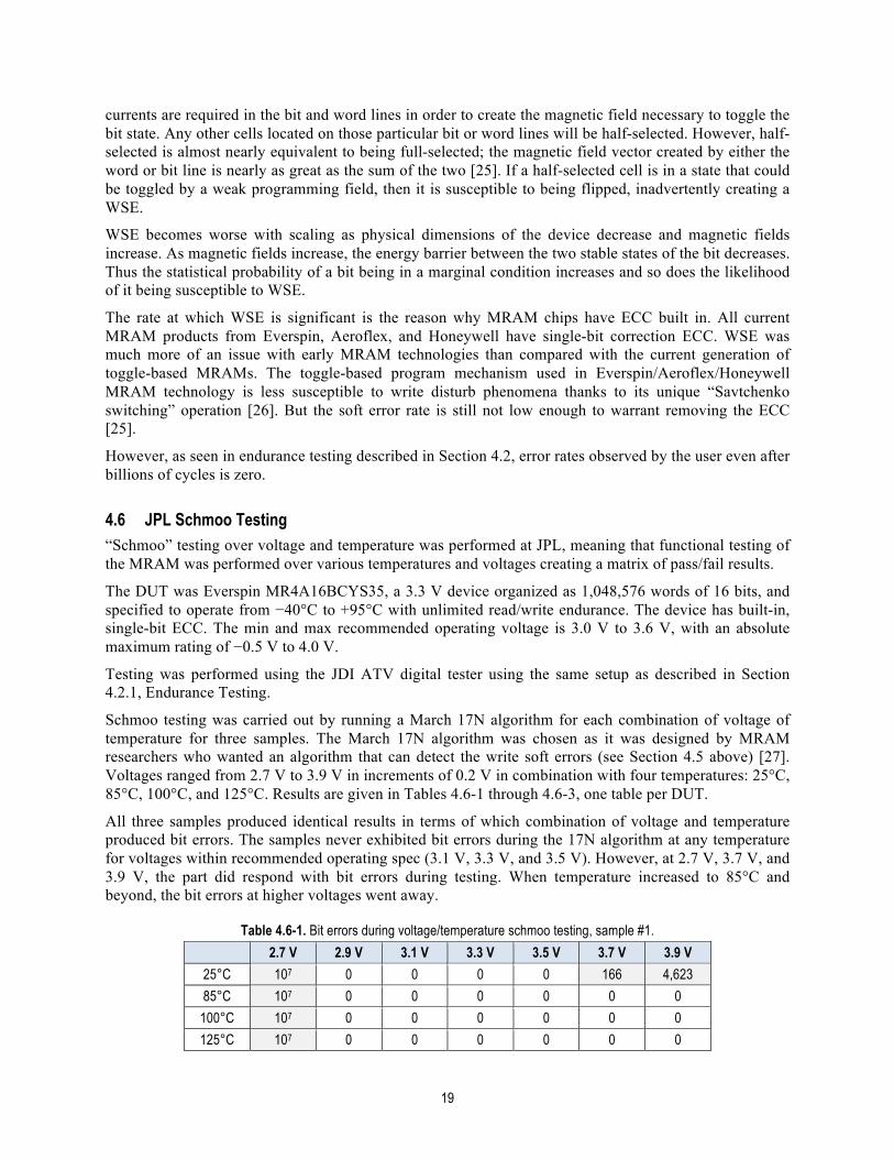
Schmoo testing was carried out by running a March 17N algorithm for each combination of voltage of temperature for three samples. The March 17N algorithm was chosen as it was designed by MRAM researchers who wanted an algorithm that can detect the write soft errors (see Section 4.5 above) [27]. Voltages ranged from 2.7 V to 3.9 V in increments of 0.2 V in combination with four temperatures: 25°C, 85°C, 100°C, and 125°C. Results are given in Tables 4.6-1 through 4.6-3, one table per DUT.
All three samples produced identical results in terms of which combination of voltage and temperature produced bit errors. The samples never exhibited bit errors during the 17N algorithm at any temperature for voltages within recommended operating spec (3.1 V, 3.3 V, and 3.5 V). However, at 2.7 V, 3.7 V, and 3.9 V, the part did respond with bit errors during testing. When temperature increased to 85°C and beyond, the bit errors at higher voltages went away.
Table 4.6-1. Bit errors during voltage/temperature schmoo testing, sample #1. 2.7 V 2.9 V 3.1 V 3.3 V 3.5 V 3.7 V 3.9 V
25°C 107 0 0 0 0 166 4,623
85°C 107 0 0 0 0 0 0
100°C 107 0 0 0 0 0 0
125°C 107 0 0 0 0 0 0
20
Table 4.6-2. Bit errors during voltage/temperature schmoo testing, sample #2. 2.7 V 2.9 V 3.1 V 3.3 V 3.5 V 3.7 V 3.9 V
25°C 107 0 0 0 0 123 4,196
85°C 107 0 0 0 0 0 0
100°C 107 0 0 0 0 0 0
125°C 107 0 0 0 0 0 0
Table 4.6-3. Bit errors during voltage/temperature schmoo testing, sample #3.
2.7 V 2.9 V 3.1 V 3.3 V 3.5 V 3.7 V 3.9 V 25°C 107 0 0 0 0 103 3,748
85°C 107 0 0 0 0 0 0
100°C 107 0 0 0 0 0 0
125°C 107 0 0 0 0 0 0
4.7 Radiation Effects Although the memory elements in an MTJ-based MRAM are inherently immune to radiation induced failure or upset, the CMOS control circuitry surrounding the memory array can be susceptible to radiation effects.
4.7.1 Commercial Everspin In 2010 JPL performed radiation effects testing on a 1 Mb commercial device from Everspin, MR0A08B [28]. Everspin moved from 150 nm to 130 nm for this device, and also introduced an epitaxial layer. The device was found to be latchup free to an effective LET of 84 MeV-cm2/mg, the maximum LET at which our testing ended. We also found the part to operate to a TID of 75 krad (Si) and, of course, to be immune to SEU due to the magnetic memory elements. Radiation performance summary for Everspin MRAM is given in Table 4.7-1.
Table 4.7-1. Radiation performance summary of Everspin commercial MRAM.
Parameter Limits Total Dose (TID) >75 krad (Si)
SEU1 >100 MeV-cm2/mg
SEL >84 MeV-cm2/mg Note:
1. Not tested by JPL.
4.7.2 Honeywell The rad-hard MRAMs from Honeywell are fabricated on rad-hard silicon-on-insulator (SOI) CMOS in order to make the CMOS control circuitry as rad hard as the memory array. The Honeywell device is very hard, with performance exceeding 1 Mrad (TID), and immunity to latchup and upset. Radiation performance summary for Honeywell MRAM is given in Table 4.7-2.
Table 4.7-1. Radiation performance summary of Everspin commercial MRAM.
Parameter Limits Total Dose (TID) >1 MRad (Si)
Soft Error Rate1 Heavy Ion/Proton
<1×10⁻¹⁰ upsets/bit-day
21
Parameter Limits Dose Rate Upset 109 rad (Si)/s
Dose Rate Survivability 1012 rad (Si)/s
Neutron Fluence >1014 N/cm2 Note:
1. Geo—solar min, 100 mils Al shielding
4.7.3 Aeroflex The rad-hard MRAMs from Aeroflex are hardened through design and process techniques. The Aeroflex device also performs very well under radiation exposure, with performance exceeding 300 krad (TID), and immunity to latchup and upset. Radiation performance summary for Aeroflex MRAM is given in Table 4.7-2.
Table 4.7-2. Radiation performance summary of Aeroflex rad-hard MRAM [22].
Parameter Limits Total Dose (TID) >300 kRad (Si)
SEL >100 MeV-cm2/mg
SEU >100 MeV-cm2/mg
22
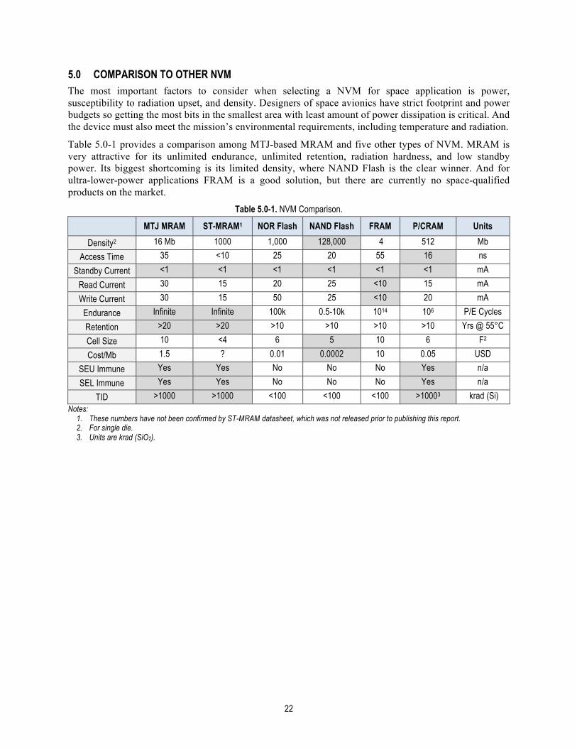
5.0 COMPARISON TO OTHER NVM The most important factors to consider when selecting a NVM for space application is power, susceptibility to radiation upset, and density. Designers of space avionics have strict footprint and power budgets so getting the most bits in the smallest area with least amount of power dissipation is critical. And the device must also meet the mission’s environmental requirements, including temperature and radiation.
Table 5.0-1 provides a comparison among MTJ-based MRAM and five other types of NVM. MRAM is very attractive for its unlimited endurance, unlimited retention, radiation hardness, and low standby power. Its biggest shortcoming is its limited density, where NAND Flash is the clear winner. And for ultra-lower-power applications FRAM is a good solution, but there are currently no space-qualified products on the market.
Table 5.0-1. NVM Comparison.
MTJ MRAM ST-MRAM1 NOR Flash NAND Flash FRAM P/CRAM Units
TID >1000 >1000 <100 <100 <100 >10003 krad (Si) Notes:
1. These numbers have not been confirmed by ST-MRAM datasheet, which was not released prior to publishing this report. 2. For single die. 3. Units are krad (SiO2).
23
6.0 FLIGHT HERITAGE
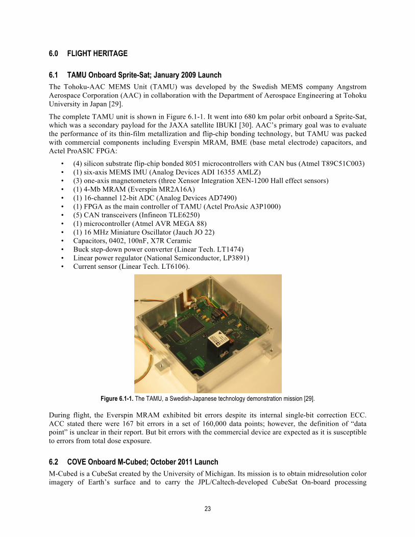
6.1 TAMU Onboard Sprite-Sat; January 2009 Launch The Tohoku-AAC MEMS Unit (TAMU) was developed by the Swedish MEMS company Angstrom Aerospace Corporation (AAC) in collaboration with the Department of Aerospace Engineering at Tohoku University in Japan [29].
The complete TAMU unit is shown in Figure 6.1-1. It went into 680 km polar orbit onboard a Sprite-Sat, which was a secondary payload for the JAXA satellite IBUKI [30]. AAC’s primary goal was to evaluate the performance of its thin-film metallization and flip-chip bonding technology, but TAMU was packed with commercial components including Everspin MRAM, BME (base metal electrode) capacitors, and Actel ProASIC FPGA:
• (4) silicon substrate flip-chip bonded 8051 microcontrollers with CAN bus (Atmel T89C51C003) • (1) six-axis MEMS IMU (Analog Devices ADI 16355 AMLZ) • (3) one-axis magnetometers (three Xensor Integration XEN-1200 Hall effect sensors) • (1) 4-Mb MRAM (Everspin MR2A16A) • (1) 16-channel 12-bit ADC (Analog Devices AD7490) • (1) FPGA as the main controller of TAMU (Actel ProAsic A3P1000) • (5) CAN transceivers (Infineon TLE6250) • (1) microcontroller (Atmel AVR MEGA 88) • (1) 16 MHz Miniature Oscillator (Jauch JO 22) • Capacitors, 0402, 100nF, X7R Ceramic • Buck step-down power converter (Linear Tech. LT1474) • Linear power regulator (National Semiconductor, LP3891) • Current sensor (Linear Tech. LT6106).
Figure 6.1-1. The TAMU, a Swedish-Japanese technology demonstration mission [29].
During flight, the Everspin MRAM exhibited bit errors despite its internal single-bit correction ECC. ACC stated there were 167 bit errors in a set of 160,000 data points; however, the definition of “data point” is unclear in their report. But bit errors with the commercial device are expected as it is susceptible to errors from total dose exposure.
6.2 COVE Onboard M-Cubed; October 2011 Launch M-Cubed is a CubeSat created by the University of Michigan. Its mission is to obtain midresolution color imagery of Earth’s surface and to carry the JPL/Caltech-developed CubeSat On-board processing
4 silicon substrate flip-chip bonded 8051 microcontroller with CAN bus (Atmel T89C51C003)
1 six-axis MEMS IMU (Analog Devices ADI 16355 AMLZ)
3 one-axis magnetometers (3 Xensor Integration XEN-1200 Hall effect sensors)
1 4 Mbit Magnetic RAM (MRAM, Everspin/Freescale MR2A16A)
In addition, ÅAC is also testing the performance of several commercial technologies that could be of great value to future low-cost nano- and microsatellites, including:
1 16-channel 12 bit ADC (Analog Devices AD7490)
1 FPGA as the main controller of TAMU (Actel ProAsic A3P1000)
5 CAN transceivers (Infineon TLE6250) 1 microcontroller (Atmel AVR MEGA 88)
controlling the IMU 1 16 MHz Miniature Oscillator (Jauch JO 22) Capacitor passives, 0402,100nF, X7R ceramic Buck step-down power converter (Linear Tech.
LT1474) Linear power regulator (National Semi.
LP3891) Current sensor (Linear Tech. LT6106)
Devices on two printed circuit boards make up the TAMU subsystem. Figures 1 to 3 shows the TAMU setup starting with the layout of the main board distribution of functions, and then the flight hardware.
Figure 1. Photograph of the TAMU bottom engineering model (EM) PCB board with the locations of components. Note the four flip-chip MCU (A-D) located on the bottom half. Based on the fact that all components on the TAMU subsystem are of commercial grade it is expected that high energy radiation events, such as Single Event Upsets (SEUs) and Single Event Latch-Ups (SELs) will occur throughout the mission.
Figure 2. Photograph of the bottom flight model (FM) PCB of TAMU. Note the four flip-chip MCU (A-D) located at the top half. The MCUs are covered with globe-top for protection of the wire bonds used to connect the Hybrid’s to the PCB.
Figure 3. Photograph of the of the complete Flight Model of TAMU including the IMU add-on PCB sitting on-top of the main PCB. TAMU uses a distributed architecture to increase the probability of detecting errors and acquire statistically significant data. Figure 4 shows a block diagram of the TAMU excluding the IMU add-on, where the CAN bus structure and serial UART (RS232) architecture are clearly seen. A large number of parameters are collected every second on TAMU and transmitted via telemetry for analysis on the ground. Table II shows the parameters that are recorded on TAMU. Based on the current measurements and cyclic redundancy checks (CRCs), it should be possible to draw conclusions on the
24
Validation Experiment (COVE). Cove included a Xilinx Virtex-5QV space-grade FPGA, Everspin MR4A16B commercial 4-Mb MRAM, and Numonyx P5QPCM commercial 128-Mb PRAM.
Unfortunately, the University of Michigan team was unable to send commands to the satellite. It is suspected that it did not properly separate from another CubeSat, Explorer 1-Prime.
6.3 Honeywell and Aeroflex Space MRAM Although Honeywell claims to have shipped over 2,000 units of their 1-Mb device, no flight heritage for Honeywell or Aeroflex is known by the author at this time. So far, at JPL, missions have shown interest in using MRAM, particularly to store FPGA images for large devices such as the Virtex-5, but nothing has flown yet or is planned to launch with MRAM. It is expected that once the higher density 16-Mb and 64-Mb devices receive DLA certification, these products will find their way into more designs.
25
7.0 CONCLUSION MRAM is a very attractive nonvolatile memory, thanks to its radiation hardness, low standby power, and unlimited endurance and retention characteristics. It may lack the density to serve as the primary science data store for some missions (NAND Flash may be a better option), but applications requiring only 64 Mb per device may find MRAM to be a superior option compared to NOR Flash, EEPROM, or one-time-programmable PROMs. Missions in the planning or design phase may want to seriously consider using MRAM.
Future generations of MRAM, such as ST-MRAM, could even become an “ideal memory,” with gigabit densities, infinite nonvolatility, unlimited endurance, and immunity to radiation effects.
26
8.0 ACKNOWLEDGEMENTS The author would like to thank Alfredo Bravo-Iniguez, Electrical Engineering student at the University of Idaho, Boise, for his extensive contributions to the endurance and schmoo testing of the 4-Mb Everspin MRAM.
27
9.0 REFERENCES [1] http://en.wikipedia.org/wiki/Magnetic-core_memory. [2] Schwee, L., et. al., “The concept and initial studies of a crosstie random access memory (CRAM),” J. Appl.
and Microstructures, vol. 4, pp. 45–50, 1988. [6] http://www.mrl.ucsb.edu/~seshadri/2012_286G/CMR.pdf. [7] G. H. Jonker and J. H. Van Santen, Physica, vol. 16, pp. 377, 1950. [8] Everspin sales brochure, http://everspin.com/PDF/MSG-14349_MRAM_Sales_Bro.pdf. [9] Ikeda, S., et. al., “Tunnel magnetoresistance of 604% at 300 K by suppression of Ta diffusion in
CoFeB/MgO/CoFeB pseudo-spin-valves annealed at high temperature,” Appl. Phys. Lett., vol. 93, 2004. [10] Everspin presentation, CES 2013, http://everspin.com/CES2013/CES_2013_Everspin_Presentation.pdf. [11] Everspin press release, November 12, 2012, http://everspin.com/PDF/ST-MRAM_Press_Release.pdf. [12] Everspin technical guide, http://everspin.com/PDF/TSP-12545_MRAM_Bro_Upd_v3db.pdf. [13] Everspin presentation, CES 2012, http://everspin.com/CES2012/CES_2012_Everspin_Slide_Show.pdf. [14] J.M.Slaughter, et. al., “Fundamentals of MRAM technology,” J. Superconduct., vol. 15, 2002. [15] Everspin toggle MRAM Web page, http://everspin.com/technology.php?qtype=3. [16] Huai, Y., “Spin-Transfer Torque MRAM: Challenges and Prospects,” AAPPS Bulletin, 2008. [17] Everspin ST-MRAM Web page, http://everspin.com/technology.php?qtype=4. [18] Honeywell MRAM Webinar, 2012. [19] Aeroflex press release, http://aeroflex.com/ams/news/2012/120628-MRAMFamily.pdf. [20] “HiRel non-volatile MRAM executive overview,” PowerPoint slides sent from Aeroflex to author, 2012. [21] Honeywell MRAM datasheets, http://www.honeywellmicroelectronics.com. [22] Aeroflex MRAM datasheets, http://www.aeroflex.com/ams/pagesproduct/prods-hirel-mems.cfm. [23] Hoberman, B., “The emergence of practical MRAM,” http://www.crocus-
technology.com/pdf/BH%20GSA%20Article.pdf. [24] Akerman, J., et. al., “Demonstrated reliability of 4-Mb MRAM,” IEEE Transactions on Device and Materials
Reliability, vol. 4, 2004. [25] DeBrosse, J., “Error detection and correction method and apparatus in a magnetoresistive random access
memory.” U.S. Patent 6,704,230, filed Jun. 12, 2003, and issued Mar. 9, 2004. [26] Grynkewich, G., et al., “Nonvolatile magnetoresistive random-access memory based on magnetic tunnel
junctions,” MRS Bulletin, vol. 29, 2004. [27] Li, J., et. al, “March-based RAM diagnosis algorithms for stuck-at and coupling faults,” Proceedings of the
IEEE International Test Conference, 2001. [28] Heidecker, J., et. al., “Single event latchup (SEL) and total ionizing dose (TID) of a 1-Mbit magnetoresistive
random access memory (MRAM),” Radiation Effects Data Workshop (REDW), 2010. [29] Bruhn, F., et. al., “Bridging the space technology ‘valley of death:’ Two spaceflights in 2009 to validate
advanced MEMS/Microtechnology systems and subsystems,” CANEUS Workshop, 2009. [30] JAXA press release, http://www.jaxa.jp/press/2009/01/20090124_ibuki_ e.html.