Page 1
N94- 36404i /
/
SIMULATION OF MATERIALS PROCESSING:FANTASY OR REALITY?
Thomas J. Jenkins
and
Victor M. Bright
Department of Electrical and Computer Engineering
Air Force Institute of Technology
Wright-Patterson Air Force BaseOhio 45433-6583
Telephone 513-255-1200, ext. 4818, or 513-255-3576 ext. 4598
IlaAClE BLJ,N_" .r_3T Ft[M_D153
https://ntrs.nasa.gov/search.jsp?R=19940031897 2018-07-19T23:42:31+00:00Z
Page 3
Simulation of Materials Processing:
Fantasy or Reality?
Thomas J. Jenkins, Capt, USAF
Victor M. Bright, PhD
Department of Electrical and Computer Engineering
Air Force Institute of Technology
Wright-Patterson Air Force Base, OH 45433-7765
KEY WORDS: computer-aided design (CAD), microelectrc,_.cs, oxidation,
computer simulation.
PREREQUISITE KNOWLEDGE: The students should understand the concepts
associated with the oxidation of silicon as applied to integrated circuit fabrication. In addition,
the students should be familiar with the operating system of the computer, which will be
executing the software.
OBJECTIVES: The objectives of this experiment are the following:
1. Introduce the general topic of simulation of materials processing as it
relates to the fabrication of microelectronic circuits,
. Familiarize the students with the use of the specific process simulation
tool, which they will be required to use during subsequent
semiconductor experiments, and
3. Introduce three independent measurement techniques which are used to
characterize oxide thickness and to verify computer simulations.
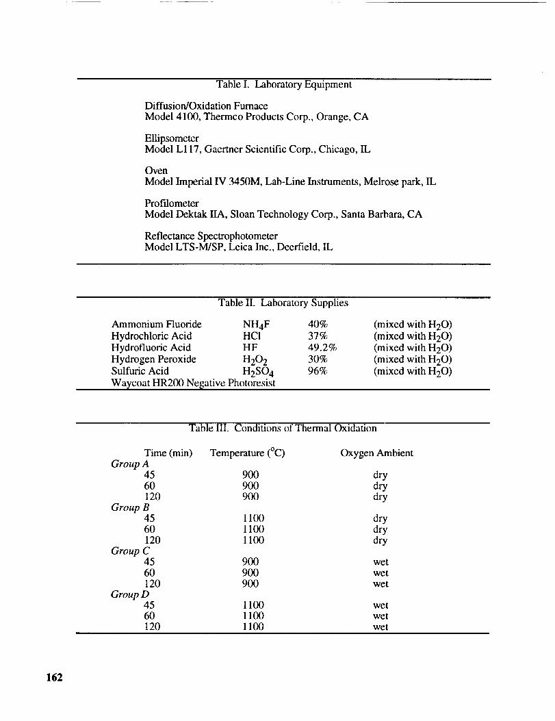
EQUIPMENT AND SUPPLIES: The equipment required to implement this
experiment is listed in Table I. The oxidation furnace is used to oxidize the silicon wafers.
The reflectance spectrophotometer, ellipsometer and profilometer are required to measure the
thickness of the resulting oxides.
The TSUPREM-4 (Technology Modeling Associates, Inc., Palo Alto, CA) simulation
software I is required. The students will use this software to simulate the various oxidation
furnace conditions utilized during the oxidation process.
PRBCtlOh"_ PAGE BkArlK NOT FILMED _ : .......... :..... • : .,--..' : _-.'_ 155
Page 4
The required processing supplies are those commonly found in a silicon-based
semiconductor research laboratory. These supplies are listed in Table II. All of the chemical
supplies should be standard electronics grade. The specific silicon wafers utilized in this
experiment are prime grade, (100)-oriented, p-type (boron doped) with a nominal resistivity of
6- 18 f2.cm.
PROCEDURE: The general procedure of this experiment consists of four steps:
1) simulation of the oxidation process, 2) thermal oxidation of silicon wafers, 3) measurement
of the resulting oxide thickness, and 4) comparison of the simulation to the actual results of the
oxidation.
1. Simulation of Oxidation Process.
To accomplish the computer simulations, the students are provided a user's guide 2 and
an introduction to the use of the TSUPREM-4 software. The user's guide briefly describes the
fundamental processes which can be simulated with the software. Practical information
concerning the trade-offs between accuracy and simulation time, as well as the basic structure
of the simulation input files, is presented. The introduction is accomplished by executing a
simple example with the students observing the flow of the simulation process. A commentary
is provided during the simulation process.
After familiarizing themselves with the software, the students simulate the thermal
oxidation of silicon for various process conditions. The various oxidation conditions are listed
in Table III. The wet oxygen ambient consists of atmospheric-pressure oxygen bubbled
through water containing 2% (by volume) HCh In addition, the furnace pressure is maintained
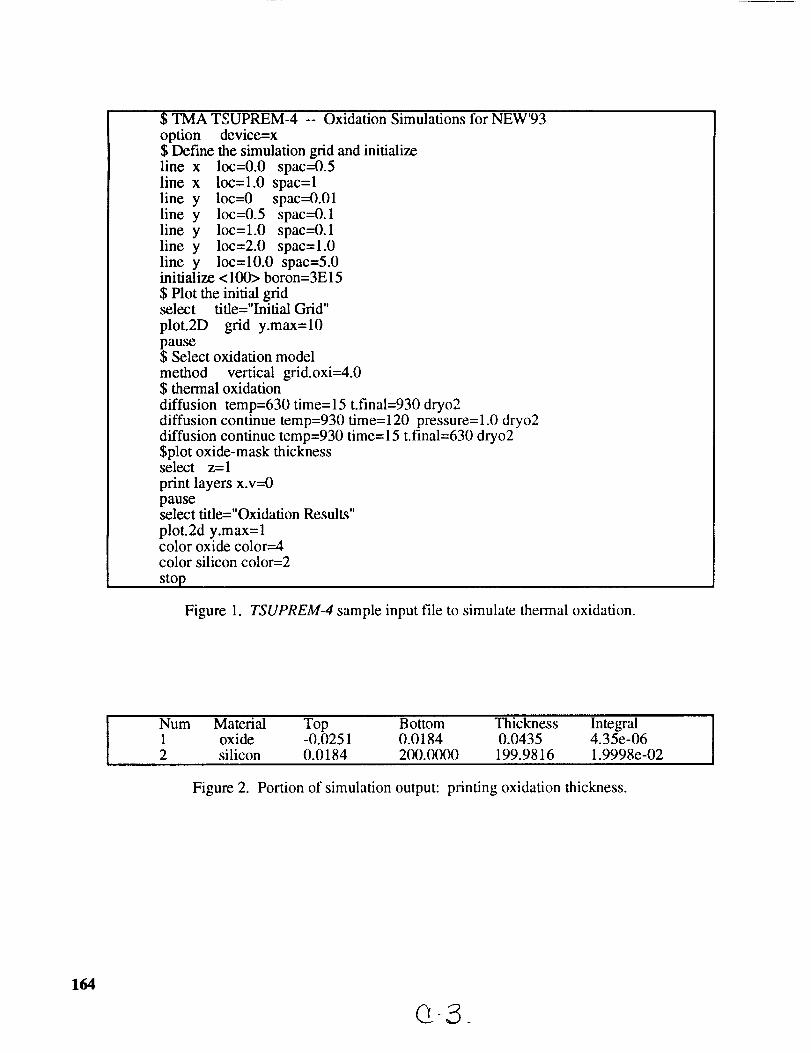
at one atmosphere during all oxidation conditions. A sample simulation file is presented in
Figure 1, and portions of the generated output are depicted in Figures 2 and 3.
2. Thermal Oxidation of Silicon Wafers.
The students implement the thermal oxidation which they previously simulated. To
accomplish this process, the students must clean the wafers and expose them to the appropriate
oxidation conditions.
(A) Cleaning:
Since undetectable traces of contaminants can be catastrophic to both the wafer and the
oxidation furnace, proper cleaning is essential before exposing the wafers to the elevated
temperatures in the oxidation furnace.
156
Page 5
(1) The wafers should be immersed in a modified piranha solution
(H2SO 4 : H202, 3:2). The wafers should be cleaned for 20 minutes and rinsed thoroughly
with deionized (DI) water to at least a 10 Mfl.cm standard.
(2) Then, after blowing the wafers dry with N2, they should be transported to
the oxidation furnace in a covered container.
(B) Oxidation:
Two types of oxygen ambients (dry and wet) will be used by the students. The wet
ambient should be realized by flowing the dry oxygen through a 2% (by volume) solution of
HC1 and DI water, which is heated to 95°C.
(1) The wafers should be loaded into a quartz oxidation boat.
(2) A furnace setting of 900°C and an oxygen flow of one liter per minute
(lpm) should be verifed.
(3) The wafer boat should then be slowly pushed (1 inch per minute) into the
furnace's center hot-zone. If a wet oxidation is to be done, the wafers should be exposed to
the dry oxygen for 5 minutes prior to flowing the wet oxygen through the furnace. This brief
dry oxidation will produce an initial thin oxide. This initial oxide will prevent the introduction
of defects in the silicon wafer which may be caused by the exposure to HCI.
(4) Upon completion of the oxidation, the wafer boat should be withdrawn
from the furnace at the rate of 1 inch per minute. The wafers should be removed from the boat
and placed in a covered container.
(5) The oxidation process is repeated for each of the process conditions.
3. Measurement of Oxide Thickness.
After completing the oxidation, the students measure the oxide thickness which was
produced during the various processing conditions. The thickness of the oxides is determined
by using a reflectance spectrophotometer, an ellipsometer and a profilometer. The reflectance
spectrophotometer and ellipsometer introduce the students to two types of non-contact,
nondestructive measurement techniques, whereas the profilometer introduces the students to
a destructive measurement technique.
While reflectance spectrophotometric and ellipsometric measurements do not require
specific post-processing of the oxidized wafers, profilometry requires the fabrication of mesas
within the oxide layer to be measured. This requirement makes profilometry destructive. To
fabricate the mesas, a simple multistep process is used. Portions of the oxide are selectively
etched. The remaining oxide forms mesas of silicon dioxide upon the silicon wafer's surface.
157
Page 6
Thesemesasaresubsequentlymeasuredwith theprofilometerto determinetheoxidethickness.Themesafabricationconsistsof thefollowingsteps:
(A) Masking:(1) WaycoatHR200negativephotoresistis dabbedontotheoxidizedwafer's
surface.A sterilecottonQ-tip is usedto applythephotoresist.Thediameterof thedotsor
specklesof photoresistshouldbelessthan5mm.(2) Thepatternedwafersareplacedin anovenat 135°Cfor 20minutesto
evaporatethesolventsfrom thephotoresistandhardenit. If anovenis notavailable,ahot
platecanbesubstituted.
(B) Etching:(1) After allowingthewafersto cool,thewafersareetchedusingabuffered
HF (NH4F: HF,4:1) solution. Freshetchantshouldbemixedsufficientlyearlyto let it
stabilize(2 hours)beforeit is used.Nevertheless,it mustbeusedwithin 6hoursaftermixing.Thewafersareetcheduntil theexposedportionsof thewaferbecomehydrophobicandall
unmaskedportionsof theoxidearecompletelyetchedaway. Studentscananticipateanetchrateof 110-150nm/min.
(2) Theetchedwafersarerinsedin DI waterfor 2 min,_tesafteretching.
(C) Stripping:
After etching,theremainingphotoresistmustbestrippedfrom thewafers'surface.(1) Thewafersareimmersedin amodifiedpiranhasolution(H2SO4 :H202,
3:2). Thewafersshouldbecleanedfor 20minutesandi'insedthoroughlywith DI water.(2) Then,afterblowingthewafersdrywith N2,theresultingmesasof silicon
dioxidecanbecharacterizedby profilometry.
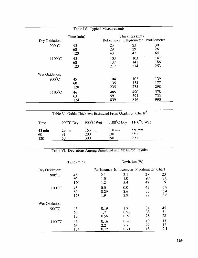
Theresultsof reflectancespectrophotometer,ellipsometer,andprofilometer
measurementsof atypicalexperimentaltrial aredepictedinTableIV. Thereflectance
spectrophotometerresultsaretheaverageof tenmeasurementsof two similarlyoxidizedwafers.Likewise,theellipsometerresultsaretheaveragevaluesof twosimilarly oxidized
wafers.Theprofilometerresultsaretheaverageof multiplemesasononeof thetwowafers,
whichwerepreviouslycharacterizedduringellipsometry.
158
Page 7
4. Analysis of the Results.
The students compare the measured oxide thickness to the simulations of the actual
fabrication process. In their analysis, the students use estimated oxide thicknesses from the
TSUPREM-4 results and oxidation charts from textbooks. As part of their analysis, the
students need to consider ease of use, accuracy, and precision of the computer simulations.
The students should "discover" the utility of CAD tools designed to model
technological processes. For example, the wet oxidation is not readily determined from simple
oxidation charts. Table V depicts the information which can be found in most oxidation charts.
While the use of HCI in the steam yields oxides with superior electrical properties, the HC1
modifies the oxidation rate of silicon. Also, the initial dry oxidation for 5 minutes (before
introducing the steam) produces an initial thin oxide which is not accounted for in most charts.
Hence, multi-step processes are more easily handled with CAD tools. Without CAD,
the students must compute the expected oxide thickness by consulting numerous tables of
parameters, such as linear and parabolic rate constants. This process can be tedious, repetitive,
and prone to errors; thus, the students realize the value of CAD.
In addition, the use of charts and other graphics requires interpolation of parameters to
account for the actual process conditions. Small deviations can affect the accuracy of the
process. For example, a deviation of 5 minutes and 10°C may yield an error of more than
10 nm. This error can be significant when working with typical microelectronic devices which
have critical oxide thicknesses of about 20 nm. These small deviations are easily entered into
CAD tools, whereas the interpolation errors in simple charts can be as large as the process
deviations. These errors can affect accuracy and precision.
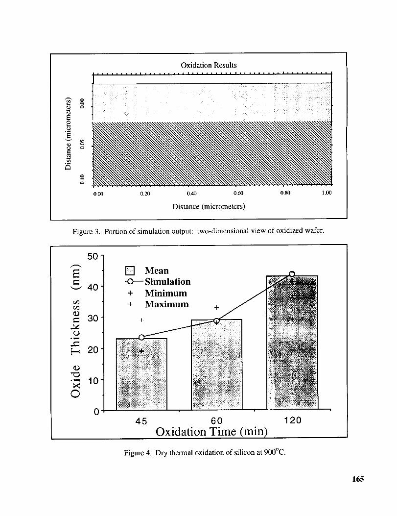
The accuracy and precision of a calibrated simulation are readily obvious to the students
after they compile figures or tables comparing simulations to measurements. Examples of
typical results are depicted in Figures 4-7 and Table VI. The dry oxidation results are depicted
in Figures 4 and 5. Additionally, the wet oxidation results are illustrated in Figures 6 and 7.
Within each figure, the simulation results are compared to the measured reflectance
spectrophotometric results. The mean measured value is depicted with a bar, while the
maximum and minimum measured values are depicted with unconnected cross symbols. The
corresponding simulated values are depicted with a connected line.
The typical magnitudes of the deviation among the simulations and measured results are
depicted in Table VI. As depicted in Table VI, the deviations among the simulations and the
nondestructive techniques of measurement are consistently less than four percent. From simple
analyses, such as these, it should be readily apparent to the students that a great deal of
variability exists. However, it should also be evident to the students that CAD produces a
result comparable to the measured values with relative ease of use.
159
Page 8
SAMPLE DATA SHEETS: Self-Evident.
INSTRUCTOR NOTES: This experiment introduces students to the application of
computer-aided design (CAD) and analysis of materials processing in the context of integrated
circuit (IC) fabrication. The fabrication of modern ICs is a complex process which consists, of
several sequential steps. These steps involve the precise control of processing variables such
as temperature, humidity, and ambient gas composition. In essence, the particular process
employed during the fabrication becomes a "recipe." Due to economic and other
considerations, CAD is becoming an indispensable part of the development of new recipes for
IC fabrication.
In particular, this experiment permits the students to explore the CAD of the thermal
oxidation of silicon. After the students simulate dry and wet oxidation processes, they
implement the simulated processes and measure the thickness of the oxide actually realized with
their recipes. The students conclude the experiment by reconciling the differences between the
simulated and real oxide.
The students should be divided into at least four groups. The groups are represented in
Table III. By assigning each group a particular oxidation condition, the individual groups of
students can complete the time consuming oxidations relatively quickly (during a single
laboratory period of three to four hours). Another laboratory period is required to complete the
measurements of the oxidation thickness. Upon completing the oxidations in the laboratory,
the four groups can share their measured results. Another laboratory _riod is required to
complete the simulations. The entire experiment can be easily incorporated within a lecture
course on integrated circuit technology. The integration of the experiment within a technology
course can provide a hands-on realistic appraisal of the utility of CAD tools in materials
processing.
The students should be cautioned about the hazards. When working with the acids, the
students should wear eye protection and gloves. Particular care should be exercised while
working with HF. When working with the ellipsometer, the students should be warned not to
stare into the laser.
Upon completion of the experiment, the students gain an insight into the role of CAD in
material processing. Hence, they can begin to discern when CAD may be intelligently applied
to processing so as not to obfuscate, but to enlighten. That is, the student will be able to
distinguish between the fantasies and the realities associated with semiconductor-material
process simulation. In addition, the student will be prepared to apply the specific process
simulator in other academic studies.
160
Page 9
REFERENCES:
° User's Manual: TMA TSUPREM-4 Two-Dimensional Process Analysis Program,
Version 9035. Technology Modeling Associates, Inc., 300 Hamilton Avenue, Third
Floor, Palo Alto, California 94301, September 1990.
. Thomas Jenkins: AFIT User's Guide to TSUPREM4, Student Handout, Department
of Electrical and Computer Engineering, Air Force Institute of Technology, Wright-
Patterson Air Force Base, Ohio 45433, December 1991.
3. Roy Colclaser: Microelectronics Processing and Device Design, John Wiley & Sons,
New York, 1980, pp. 92-93.
SOURCES OF SUPPLY: Other than the photoresist, all laboratory
chemicals required for this experiment are available from Mallinckrodt, Inc., Science Products
Division, Paris, Kentucky. The photoresist is available from Olin Hu:_t Specialty Products,
Inc., 5 Garret Mountain Plaza, West Paterson, New Jersey. The silicon wafers can be
obtained from Ziti, Inc., 14755 Preston Road, Suite 421, Dallas, Texas.
161
Page 10
TableI. LaboratoryEquipment
Diffusion/OxidationFurnaceModel 4100,ThermcoProductsCorp.,Orange,CA
EllipsometerModelL117, GaertnerScientificCorp.,Chicago,IL
OvenModel ImperialIV 3450M,Lab-LineInstruments,Melrosepark,IL
ProfilometerModelDektakl/A, SloanTechnologyCorp.,SantaBarbara,CA
ReflectanceSpectrophotometerModelLTS-M/SP,LeicaInc.,Deerfield,IL
TableII. LaboratorySupplies
AmmoniumFluoride NH4F 40%HydrochloricAcid HCI 37%HydrofluoricAcid HF 49.2%HydrogenPeroxide H202 30%SulfuricAcid H2SO4 96%Wa_,coatHR200NegativePhotoresist
(mixedwith H20)(mixedwith H20)(mixedwith H20)(mixedwith H20)(mixedwith H20)
TableIII. Conditionsof ThermalOxidation
Time(min) Temperature(°C) OxygenAmbientGroup A
45 900 dry60 900 dry120 900 dry
Group B45 1100 dry60 1100 dry120 1100 dry
Group C45 900 wet60 900 wet120 900 wet
Group D45 1100 wet60 1100 wet120 1100 wet
162
Page 11
DryOxidation:900°C
1100°C
WetOxidation:900°C
ll00°C
Table IV.
Time (min)
Typical Measurements
Thickness (nm)
Reflectance Ellipsome_r Profilome_r
45 23 23 3060 29 29 26120 43 42 64
45 103 103 14760 137 141 186123 212 214 253
45 104 102 13960 135 134 177120 235 235 298
46 485 490 57863 591 594 733124 839 846 990
Table V. Oxide Thickness Estimated From Oxidation Charts 3
Time 900°C Dry 900°CWet ll00°C Dry ll00°CWet
45 min 29 nm 150 nm 110 nm 550 nm60 31 200 130 650120 50 300 190 900
Table VI. Deviations Among Simulated and Measured Results
Dry Oxidation:
900°C
ll00°C
Wet Oxidation:
900°C
1100°C
Time (min) Deviation (%)
Reflectance Ellipsometer Profilometer Chart
45 2.1 2.1 28 2360 1.0 1.0 9.4 8.0120 1.2 3.4 47 15
45 0.0 0.0 43 6.860 0.29 2.6 35 5.4123 1.9 2.9 22 8.6
45 0.19 1.7 34 4560 1.7 0.98 33 51120 0.56 0.56 28 28
46 0.16 0.86 19 1363 2.2 2.7 27 12124 0.12 0.71 18 7.1
163
Page 12
$ TMA TSUPREM-4 -- Oxidation Simulations for NEW'93
option device=x$ Def'me the simulation grid and initializeline x loc=0.0 spac=0.5line x loc=l.0 spac=lline y loc=0 spac--0.01line y loc=0.5 spac=0.1line y loc=l.0 spac=0.1line y loc=2.0 spac=l.0line y loc=10.0 spac=5.0initialize < 100> boron=3E15
$ Plot the initial gridselect tifle="Initial Grid"
plot.2D grid y.max=10
pause$ Select oxidation model
method vertical grid.oxi=4.0$ thermal oxidation
diffusion temp=630 time=15 t.final=930 dryo2diffusion continue temp=930 time=120 pressure=l.0 dryo2diffusion continue temp=930 time=15 t.final=630 dryo2$plot oxide-mask thicknessselect z=l
print layers x.v--0pauseselect title="Oxidation Results"
plot.2d y.max=lcolor oxide color=4color silicon color=2
stop
Figure 1. TSUPREM-4 sample input file to simulate thermal oxidation.
Num
12
Material Top Bottom Thickness Integraloxide -0.0251 0.0184 0.0435 4.35e-06silicon 0.0184 200.0000 199.9816 1.9998e-02
Figure 2. Portion of simulation output: printing oxidation thickness.
164
Page 13
EoI=_
°*==t
d
. ,....1
Oxidation Results• . • • | • | | | I | • • | . | . • | I | | | i | • | | | n i . | | | | | | i l . • . • • • • | •
i_I _ _ ii i_ i
0.200.00 0.40 0.60 0.80 1.00
Distance (micrometers)
Figure 3. Portion of simulation output: two-dimensional view of oxidized wafer.
5O
40
ra_
_O= 3O
,._¢D
._=._
2O
• *..=,1
©10
Mean
-O---Simulation
+ Minimum
+ Maximum +
045 60
Oxidation Time imin)
120
Figure 4. Dry thermal oxidation of silicon at 900°C.
165
Page 14
raO
¢3° _,,,I
©
° _,,,i
©
200'
150
100
!_ Mean
-O--- Simulation
+ Minimum
+ Maximum
+
5O
045 60 123
Oxidation Time (min)Figure 5. Dry thermal oxidation of silicon at 1100°C.
raOrue3
_D
¢3° _,,-I
[.-,
°_,=1
©
3OO
25O
200
150
100
50
0
Mean
-O--- Simulation
+ Minimum
+ Maximum
45 60
Oxidation Time (min)Figure 6.
120
Wet thermal oxidation of silicon at 900°C.
166
Page 15
¢J'j
_D
° _,,,,q
©
90O
8OO
700'
600
Mean-O--- Simulation
+ Minimum+ Maximum
500
40046 63
Oxidation Time mini i
124
Figure 7. Wet thermal oxidation of silicon at 1100°C.
167