The ability to fabricate structures from the micro- to thenanoscale with high precision in a wide variety of materials isof crucial importance to the advancement of micro- and nano-technology and the nanosciences. The semiconductor industryhas been pushing high-precision nanoscale lithography tomanufacture ever-smaller transistors and higher-density inte-grated circuits (ICs). Critical issues, such as resolution, relia-bility, speed, and overlay accuracy, all need to be addressed inorder to develop new lithography methodologies for such de-manding, industrially relevant processes. On the other hand,less stringent conditions are found in many other areas, for ex-ample, photonics, micro- and nanofluidics, chip-based sensors,and most biological applications. Several alternative ap-
proaches towards nanostructure fabrication have beenexploited in the past 15 years, without resorting to expensivetools such as those used in deep-UV projection lithographyand electron-beam lithography. These techniques includemicrocontact printing (or soft lithography),[1] nanoimprintlithography (NIL),[2] scanning-probe-based techniques (e.g.,atomic force microscope lithography),[3] and dip-pen lithogra-phy.[4] A good overview of several of these techniques waspresented in a recent paper.[5] This article will focus on NILtechnology and review the progress that has been made in thisfield in recent years. Nanoimprinting can not only create resistpatterns, as in lithography, but can also imprint functional de-vice structures in various polymers, which can lead to a widerange of applications in electronics, photonics, data storage,and biotechnology. Some of these applications have been dis-cussed in a previous review.[6]
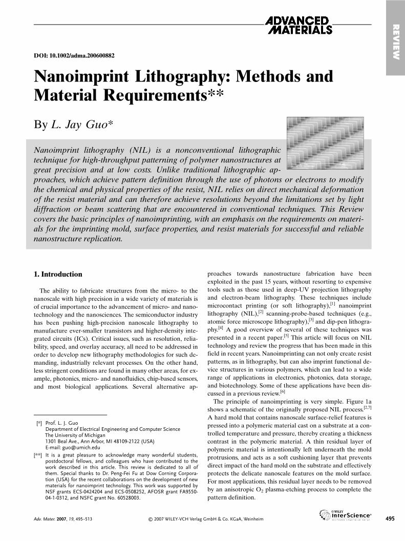
The principle of nanoimprinting is very simple. Figure 1ashows a schematic of the originally proposed NIL process.[2,7]
A hard mold that contains nanoscale surface-relief features ispressed into a polymeric material cast on a substrate at a con-trolled temperature and pressure, thereby creating a thicknesscontrast in the polymeric material. A thin residual layer ofpolymeric material is intentionally left underneath the moldprotrusions, and acts as a soft cushioning layer that preventsdirect impact of the hard mold on the substrate and effectivelyprotects the delicate nanoscale features on the mold surface.For most applications, this residual layer needs to be removedby an anisotropic O2 plasma-etching process to complete thepattern definition.
Nanoimprint lithography (NIL) is a nonconventional lithographictechnique for high-throughput patterning of polymer nanostructures atgreat precision and at low costs. Unlike traditional lithographic ap-proaches, which achieve pattern definition through the use of photons or electrons to modifythe chemical and physical properties of the resist, NIL relies on direct mechanical deformationof the resist material and can therefore achieve resolutions beyond the limitations set by lightdiffraction or beam scattering that are encountered in conventional techniques. This Reviewcovers the basic principles of nanoimprinting, with an emphasis on the requirements on materi-als for the imprinting mold, surface properties, and resist materials for successful and reliablenanostructure replication.
–[*] Prof. L. J. Guo
Department of Electrical Engineering and Computer ScienceThe University of Michigan1301 Beal Ave., Ann Arbor, MI 48109-2122 (USA)E-mail: [email protected]
[**] It is a great pleasure to acknowledge many wonderful students,postdoctoral fellows, and colleagues who have contributed to thework described in this article. This review is dedicated to all ofthem. Special thanks to Dr. Peng-Fei Fu at Dow Corning Corpora-tion (USA) for the recent collaborations on the development of newmaterials for nanoimprint technology. This work was supported byNSF grants ECS-0424204 and ECS-0508252, AFOSR grant FA9550-04-1-0312, and NSFC grant No. 60528003.
What makes NIL an attractive and widely researchedtechnology is that it demonstrated ultrahigh resolutions soonafter its inception. Figure 1b and c shows scanning electronmicroscopy (SEM) images of a mold with a pillar array(pillar diameter 10 nm) and an imprinted 10 nm hole array inpoly(methyl methacrylate) (PMMA) that were obtainedalmost a decade ago.[8] NIL is inherently high-throughput, be-cause of parallel printing, and it requires only a simple equip-ment set-up, leading to low-cost processes. A variation of theNIL technique that uses a transparent mold and UV-curableprecursor liquid to define the pattern (step-and-flash imprintlithography (SFIL), Fig. 2a) was developed soon after,[9,10]
allowing the process to be carried out at room temperatureand making it very attractive for IC semiconductor devicemanufacturers.[11]
Because of its fast development in the past decade and itspotential for sub-50 nm lithography, the Massachusetts Insti-tute of Technology’s “Technology Review” listed NIL as oneof 10 emerging technologies that will strongly impact theworld.[12] In 2003 the International Technology Roadmap forSemiconductors (ITRS) also announced the inclusion of NILonto their roadmap as a candidate technology for future ICproduction. Significant efforts from both academia and indus-try have been put in SFIL research and development,[9] tem-plate-fabrication methods,[13,14] and defect analysis.[14,15] Fig-ure 2b and c shows 20 nm lines printed by SFIL and 40 nmlines printed with a template used over 1500 times, respective-
ly. An overlay accuracy of 50 nm has been achieved by usinginterferometric in situ alignment techniques.[16] Higher de-grees of accuracy can also be anticipated.
Although NIL-based approaches have proven excellent re-solutions, there are still significant challenges in meeting thestringent requirements of semiconductor IC manufacturing,especially in terms of defect control and production-levelthroughput, which requires printing 60–80 wafers per hourwith extremely high yields. On the other hand, because of itssimplicity this technique has found numerous applications inelectronics (e.g., hybrid plastic electronics,[17] organic elec-tronics and photonics,[18,19] nanoelectronic devices in Si[20,21]
and in GaAs[22]), in photonics (e.g., organic lasers,[23] conjugat-ed[24] and nonlinear optical polymer nanostructures,[25] high-resolution organic light-emitting diode (OLED) pixels,[26,27]
diffractive optical elements,[28] broadband polarizers[29–31]),in magnetic devices (e.g., single-domain magnetic struc-tures,[32,33] high-density patterned magnetic media and high-capacity disks,[34,35,36]), in nanoscale control of polymer crys-tallization,[37] and in biological applications (e.g., manipulatingDNA in nanofluidic channels,[38,39] nanoscale protein pattern-ing,[40,41] the effect of imprinted nanostructures on cell cul-ture[42]).
Because nanoimprint lithography is based on the mechani-cal molding of polymer materials, which is drastically differentfrom other traditional lithographic techniques, it faces a newset of issues and challenges. In the following, a detailed discus-
L. Jay Guo is an associate professor of Electrical Engineering and Computer Science at the Uni-versity of Michigan. He has been involved in the development of nanoimprint technology since1996 and has exploited numerous applications in electronic and photonic devices. He obtainedhis B.S. degree from Nankai University (China) in 1990, and M.S. and Ph.D. degrees from theUniversity of Minnesota (USA) in 1995 and 1997, respectively. His Ph.D. thesis was on semicon-ductor single-electron transistors and memories. From 1997 to 1999, he was a research associatefellow at Princeton University (USA). His current research interests include the development andapplications of imprinting and printing techniques to the fabrication of functional nanostruc-tures, the study of plasmonic nanophotonics and photonic microresonators for biosensing appli-cations, research on organic LEDs and photovotaics, and the study of nanofluidic devices. Hisearlier work on room-temperature operation of silicon single-electron memory was cited by theAmerican Physical Society as one of the breakthroughs in Nanotechnology in 1997.
b)a) c)
Figure 1. a) Schematic of the originally proposed NIL process. b) Scanning electron microscopy (SEM) image of a fabricated mold with a 10 nm diam-eter array. c) SEM image of hole arrays imprinted in poly(methyl methacrylate) by using such a mold. Reproduced with permission from [8]. Copyright1997 American Institute of Physics.
sion of the requirements on the mold and resist will bepresented. Critical issues in the imprinting, separation, andetching steps will be identified, and solutions to overcome thevarious technical challenges will be described. The effective-ness of these approaches in making NIL a successful technolo-gy will be illustrated by providing ample examples.
2. NIL Mold
The elements required for NIL are (i) a mold with pre-defined surface relief nanostructures, and (ii) a suitable resistmaterial that can be deformed and hardened to preserve theshape of the impression. Usually, the resist material is appliedon top of a substrate. The mold used in NIL can essentially beany type of solid material that has a high strength and durabil-ity. The resist material can be a thermal plastic, thermal set-ting, or low-viscosity precursor that can be cured either ther-mally or by UV light. The molds or stamps are normally madein silicon, dielectric materials (e.g, silicon dioxide or silicon ni-tride), metals (e.g., nickel), or polymeric materials that have asufficient Young modulus. Common features of these differ-ent molds are that they are hard and have a high mechanicalstrength. The properties of these hard molds contrast those ofelastomeric stamps used in soft lithography, and are essentialfor producing nanoscale features because the protrusion pat-terns on the mold should not deform, buckle, or collapse dur-ing imprinting, even at elevated temperatures. In this manner,preservation of the shape and aspect ratio as well as faithfulpattern definition at size scales of 10 nm and below is guaran-teed. These requirements do not exclude the use of a flexible
backplane supporting the hard surface relief structure. It isactually advantageous for the mold to have global flexibilityand local rigidity in many applications, especially when thesubstrate is not flat, because a flexible mold can providelarge-area conformal contact with the substrate without re-sorting to high pressures. The rigiflex-mold approach expli-citly exploits this feature for NIL patterning.[43]
2.1. Mold Fabrication
Considerations for selecting mold materials include hard-ness, compatibility with traditional microfabrication process-ing or the intended applications, and the thermal expansioncoefficient of the material, to name an important few. Candi-date materials include Si, SiO2, SiC, silicon nitride, metals,sapphire, and diamond film. Work from many groups hasshown that Si and SiO2 have sufficient hardness and durabilityproperties for nanoimprint applications. The thermal expan-sion coefficient is especially important in the NIL process,where a temperature of more than 100 °C is typically requiredat the imprinting step. A thermal mismatch between the moldand the substrate could result in pattern distortions or stressbuild-up during the cooling cycle, which would affect thepattern fidelity and registration accuracy. In this regard, a Simold together with a Si substrate makes a good pair for theNIL process in applications that demand precise, criticaldimensions and overlay control. The thermal expansionmismatch can be ignored if the NIL process is carried out atroom temperature, for example, in UV-assisted NIL, room-temperature NIL,[44] or SFIL processes.
Figure 2. a) Schematic outline of the SFIL process. b) Pattern of 20 nm lines patterned by using SFIL. c) Pattern of 40 nm lines printed with a templateused over 1500 times. d,e) Multitiered SFIL template and the resulting imprint in a resist material. Reproduced with permission from [10]. Copyright2005 International Society of Optical Engineering.
The fabrication of the Si mold is straightforward if one hasaccess to other lithographic processing and reactive ion etch-ing (RIE) facilities. The commonly used processing steps areillustrated in Figure 3a. First, a resist material is spin-coatedonto the mold surface (either a pure Si substrate or Si with athermally grown oxide), followed by lithography to define the
desired mold pattern. For the lithography step, one canchoose from UV lithography for microscale and larger fea-tures, electron-beam lithography for very small features, inter-ference lithography for large-area periodic features, or NILitself. A hard masking layer, such as a metal, can be depositedover the patterned resist template, followed by a lift-off pro-cess that removes the resist template and the material on top,leaving a patterned mask layer on the Si substrate. Next, ananisotropic RIE process is used to selectively etch away the Simaterial in the unmasked region, producing the surface reliefstructures required for NIL. Figure 3b shows an SEM imageof a fabricated Si mold with protrusion features etched into athermal oxide layer grown on top of a Si substrate. Figure 4shows other examples where molds with different periodical
Figure 3. a) Schematic illustration of the Si mold-fabrication process.b) SEM image of a mold fabricated using thermally grown SiO2 on a sub-strate, with equal line widths and spacings; scale bar: 500 nm. (Theroughness seen on top of the etched oxide originates from the metal maskused in the reactive-ion-etching process that has not yet been removed).
a)
b)
c)
500 nm
Figure 4. SEM images of large-area molds with arrays of different features.a) A pillar array, produced by imprinting twice with the same grating moldbut orthogonal directions. b) A bar array, produced by two grating moldswith different periods; scale bar: 500 nm. c) Diamond-shaped array, pro-duced by two imprints that use the same grating mold but are orientedat an angle of 60°.
features were fabricated by using a grating mold and per-forming NIL twice, at orientations of either 90° or 60° withrespect to each other, followed by metal deposition, lift-off,and finally RIE to produce the desired mold features. Thesetype of molds can cover large areas (several square centi-meters) because the initial grating mold is fabricated by holo-graphic interference lithography. These molds have been usedin our group to fabricate uniform and oriented metal nano-particle arrays for studying localized surface plasmon reso-nances.[45]
Molds or templates for SFIL can be fabricated by similarmethods. However, because SFIL requires a transparent tem-plate (typically quartz or silica) a charging effect could occurduring the electron-beam lithography process, because of thenonconductive nature of these dielectric materials. Thischarging effect can severely distort the electron beam and af-fect the pattern resolution and fidelity. Several methods havebeen used to eliminate this effect. One method involvescoating a thin metal layer (e.g., 15 nm Cr) on top of the quartzsubstrate before spin-coating the e-beam resist to help dis-charge the electrons.[13] An advantage of this approach is thatthe Cr layer can be used directly as an etch mask in the sub-sequent RIE step to form features in the quartz template. Asecond method is to deposit a transparent conductive oxidelayer, such as indium tin oxide (ITO), to function as both adischarge layer and as an integral part of the template struc-ture itself.[14] The charging effect is then not only suppressedin the e-beam lithography step during template fabricationbut also at the final inspection stage by SEM, which greatlyfacilitates the manufacturing of the mold and the template.These two methods have been used to fabricate SFIL tem-plates on standard photomask plates. The second methodoffers an additional advantage, in that multiple layers ofITO can be deposited to fabricate a 3D tiered structure. Anexample is shown in Figure 2d, showing a three-layer tem-plate structure. Figure 2e shows the imprinted pattern ob-tained after using such a mold. This approach can truly takeadvantage of the mechanical molding nature of the NIL pro-cess, and can produce 3D patterns in polymers in a single step.
Ultrahigh-resolution NIL has been demonstrated by Austinet al. through the use of a specially prepared mold, consistingof a superlattice structure grown on a GaAs substrate by mo-lecular beam epitaxy. After the sample is cleaved, the exposedside is immersed in a chemical etchant that selectively etchesone component, creating a relief structure on the sample edge.By using this special mold the authors demonstrated the im-printing of 14 nm pitch patterns.[46] Tormen et al. presentedinteresting results by using a technique that allows the pro-duction of tightly controlled nano- to microscale 3D pro-files.[47] Finally, it is also possible to use the focused ion beam(FIB) technique to directly “carve out” the desired mold fea-tures, even 3D or gray-scale patterns that are very difficult tofabricate, or would involve multiple steps to obtain, by otherlithographic techniques. An example of such a structure fabri-cated by FIB is shown in Figure 5. FIB may find many uses inNIL-related applications in the future.
2.2. Mold Surface Preparation
A mold for imprint lithography typically has a high densityof nanoscale protrusion features on its surface. This effec-tively increases the total surface area that contacts the im-printed polymer, leading to strong adhesion of the imprintedpolymer to the mold. This effect can easily be seen by thesticking of a resist material to a mold without any specialtreatment. Solutions to this problem are (i) incorporating aninternal release agent into the resist formulation (as is done inthe precursor mix used for SFIL), (ii) applying a low-surface-energy coating to the mold to reduce its surface energy (or acombination of both approaches), and (iii) choosing a moldmaterial with an intrinsically low surface energy. The mostwidely adopted approach is to form a self-assembled mono-layer of a fluorosilane release agent on the mold surface (e.g.,1H,1H,2H,2H-perfluorodecyl-trichlorosilane), either by asolution-phase or a vapor-phase reaction. This approach canbe readily applied to oxide surfaces, or to Si surfaces that havebeen oxidized with a piranha soak to generate the requiredterminal hydroxyl groups. Jung et al. compared the substratestreated by the two different processes by atomic force micros-copy (AFM), ellipsometry, IR spectroscopy, and contact-anglemeasurement, and concluded that the vapor-phase coatingmethod provided superior surface-release properties.[48] Re-cently, Schift et al. found that the antiadhesion properties ofmold surfaces coated with fluorinated trichlorosilanes can befurther improved by co-deposition of monochlorosilanes.[49]
This is because the introduction of monochlorosilanes helpsto reduce the steric hindrance between the trichlorosilanemolecules bound to the mold surface, resulting in a bettermolecular packing compared to coatings that use only tri-chlorosilane molecules. It has been shown experimentally thatfluorosilane-treated molds can be used to imprint severalhundreds to a thousand times before their antiadhesion prop-erties degrade and a new coating is required.
2.3. Flexible Fluoropolymer Mold
The durability issue of the surface coating on a mold can bealleviated if the mold itself is made from a material that has a
Figure 5. Mold fabricated by using FIB, showing a gray-scale pattern (anNSF logo).
low surface energy and sufficient mechanical strength. Leeet al. have demonstrated that molds made from amorphousfluoropolymers, such as Teflon AF 2400 (glass transitiontemperature (Tg) 240 °C), can be used as mold without anysurface treatment. Teflon AF 2400 is a copolymer of 2,2-bis-trifluoromethyl-4,5-difluoro-1,3-dioxole and tetrafluoroethyl-ene.[50] The polymer has a tensile modulus of ca. 1.6 GPa (al-most a thousand times harder than the elastomeric PDMSmaterial), which is stiff enough for patterning small featureswithout mold deformation. Also, the inert nature with a lowsurface energy of 15.6 dyn cm–1 (cf. PDMS, ca. 19.6 dyn cm–1)makes it easy to demold after the imprinting process withoutany surface treatment and without deterioration in surfaceproperties over many imprinting cycles.
Mold fabrication can also be simplified by casting the fluo-ropolymer solutions over a prefabricated template and dryingoff the solvent,[51] or by direct molding or imprinting of thefluoropolymer at 350 °C under high pressure.[52] A flexiblefilm can provide a better conformal contact with the substrateto be patterned and reduce the pressure needed during theimprinting step. A further benefit is that de-molding can beachieved by pealing the mold from the imprinted substratewith an effectively smaller de-molding area. This is much easi-er than the de-molding of a stiff mold, where the hard moldneeds to be separated from the substrate as a whole. Figure 6ashows patterned high-aspect-ratio features obtained by usinga Teflon AF film mold and a UV-curable polyurethane acry-late prepolymer.[50] We have utilized another fluoropolymer
mold, ETFE or “Tefzel” (Dupont), which is a copolymer ofethylene and tetrafluoroethylene, that can be fabricated byimprinting using a hard template at a lower temperature ofca. 200 °C. Figure 6b shows a grating pattern in a UV-curableepoxysilicone liquid resist[52] imprinted by using the ETFEmold. A useful property of these fluoropolymers is that theycan be used to make “copies” of the original mold, which maybe difficult or expensive to fabricate. Recently, Choi et al.demonstrated a fluorinated organic–inorganic hybrid moldwith thermal stability to over 350 °C by using a nonhydrolyticsol–gel process.[53]
3. NIL Resist
Because imprint lithography makes a conformal replica ofthe surface relief patterns by mechanical embossing, the resistmaterials used in imprinting need to be easily deformableunder an applied pressure and should have a sufficient me-chanical strength as well as good mold-releasing properties tomaintain their structural integrity during the de-molding pro-cess. For some applications, good etching properties are re-quired for a subsequent RIE process.
Two material properties are important for the imprintingprocess. The resist material should have a Young’s moduluslower than that of the mold during imprinting. The minimalpressure required to perform the imprint should be higherthan the sheer modulus of the polymer.[54] On the other hand,the low modulus of the resist material is necessary for it to bedeformed by the mold. To complete the imprinting processwithin a practical time frame, the resist material should alsohave a sufficiently low viscosity.[55] This requirement can beeasily understood by considering the squeezed flow of a New-tonian liquid between plates that have a radius R and a gapdistance of d.[56] Such a model can approximate a processwhere a mold protrusion with size R is imprinted into a resistof an initial thickness d on a substrate. One can obtain a sim-ple solution that expresses the pressure (P) needed to obtaina certain imprinting speed (dh/dt) in terms of these dimen-sions and the fluid viscosity g: P = (3gR2/4d3)(dh/dt). A numer-ical simulation based on the finite-difference method usingthe non-steady-state Navier–Stokes equation has also givensuch a relationship for simple periodic mold features.[57] Inte-grating this equation can give the time required to halve thethickness of the fluidic layer (i.e., to imprint halfway throughthe feature height): t = 9hR2/16Pd2. This simple analysis statesthat under a fixed pressure the imprinting time scales linearlywith viscosity and quadratically with the pattern size. There-fore, the time required to imprint large-size patterns will besignificantly longer than that required for nanoscale patterns.
3.1. Thermal Plastic Resists
For the plastic materials used in the thermal NIL process,the two requirements mentioned in the previous paragraphcan be met simultaneously by raising the temperature abovethe glass transition temperature (Tg) of the polymer, so thatboth Young’s modulus and the viscosity will drop by severalorders of magnitude compared to their respective values atroom temperature (Young’s modulus for glassy polymers justbelow Tg is approximately constant over a wide range of poly-mers, at ca. 3 × 10⁹ Pa). In practice the temperature chosenfor NIL is ca. 70–90 °C above the Tg, so that the polymer ma-terial reaches a viscous flow state.[6] In thermal NIL the moldand the imprinted polymer must be cooled to below the Tg ofthe polymer to preserve the imprinted pattern after the moldis removed. Because the Tg is the onset temperature for mo-
Figure 6. a) SEM image of 80 nm dense lines in a photocurable prepoly-mer solution molded by using a Teflon AF mold; scale bar: 1 lm. Repro-duced with permission from [50]. Copyright 2004 American ChemicalSociety. b) SEM image of a 700 nm periodiocal grating structure in aUV-curable resist, imprinted by using a flexible sheet of a copolymer ofethylene and tetrafluoroethylene (ETFE) as a mold; scale bar: 2 lm [52].
lecular motion in polymers, factors that increase the energyrequired for molecular motion (e.g., intermolecular forces,intrachain steric hindrance such as branching or crosslinking,and bulky and stiff side groups) also increase the Tg value;those factors that decrease the energy requirement (e.g., flex-ible bonds, flexible side groups) lower the Tg. These consid-erations can be exploited in choosing the desired Tg for theimprint resists. For many applications, it is desirable to use alower temperature in processing. A reduction in temperaturehas to be compensated by corresponding increases in imprint-ing pressure and time to obtain satisfactory results.[58]
There is a trade-off between the imprinting temperatureand the thermal stability, which is illustrated in the followingexample for polymers with different Tg values. Figure 7ashows patterns imprinted in poly(benzyl methacrylate) (mo-lecular weight (Mw) ca. 70 000 g mol–1, Tg = 54 °C) at a tem-perature of 134 °C, and Figure 7b shows patterns imprinted inpoly(cyclohexyl acrylate) (Mw ≈ 150 000 g mol–1, Tg = 19 °C) at99 °C. In both cases an imprinting temperature of Tg + 80 °Cwas chosen, and the applied pressure was 5 MPa. Very goodpattern definitions were obtained. Although a low-Tg materialcan be used in NIL for the sake of reducing the processingtemperature, the imprinted patterns are also unstable andtend to deform at temperatures close to the imprinting tem-perature. Figure 7c shows pattern relaxation at room temper-ature, observed 10 days after the structure in Figure 7b wasimprinted (in this case the resist had a Tg of 19 °C, which isbelow room temperature). The patterned structures will relaxfaster at elevated temperatures, such as those encountered ina RIE chamber during subsequent removal of residual resistor pattern transfer into a substrate. Various alternatives havebeen exploited to lower the viscosity of thermoplastic materi-als, rendering them imprintable at temperatures close to roomtemperature. These include dissolving the polymer in itsmonomer[59] or another solvent and using a PDMS stamp forsolvent evaporation.[60] From the example given above, it canbe inferred that thermally curable or thermosetting polymersare excellent resist systems for NIL because of the possibilityof low-pressure imprinting and good mechanical integrityafter crosslinking by thermal treatment. An example of such asystem is described in the following section.
The viscosity of a polymer material not only depends on thetemperature, but also depends strongly on the polymer’s Mw
relative to the so-called critical molecular weight (Mc) of agiven polymer. The Mc can be interpreted as the molecularweight at which a temporary network of entanglements spansover macroscopic dimensions. In practice, low-molecular-weight polymers with Mw < Mc can be imprinted at lower tem-peratures, lower pressures, or within shorter times. However,the absence of such a network of entanglements may lead tomore brittle behavior, and could result in the fracture of theimprinted polymer features during the mold-separation step.Therefore, the choices of Tg and Mw are both important inmaintaining the structural stability of the imprinted patterns.In addition, the stress build-up resulting from the appliedpressure at a temperature below Tg after imprinting couldstrongly affect the integrity of the polymer pattern duringmold separation. Hirai et al. have investigated this problem indetail.[61] For more discussions on material rheology issues re-lated to NIL, the readers are referred to Chapters 3 and 4 inan earlier publication.[56]
3.2. UV-Curable Resists
The high temperatures and pressures required for the nano-imprinting of thermoplastic materials could limit the through-put and application scope of the NIL technique. In addition,the thermal expansion mismatch between the mold and thesubstrate often presents an obstacle for pattern overlay overlarge substrates. An alternative is to use liquid precursors thatcan be cured by UV light at ambient temperatures. For suchmaterials, the low Young modulus and low viscosity require-ments are naturally satisfied. Because of the low viscosity ofthe monomer fluid the imprinting process is less sensitive tothe effects of pattern density reported for NIL. Furthermore,the process allows the use of a small-area mold and the pat-terning of large-area substrates by a step-and-repeat process,similar to SFIL. The liquid resist developed for SFIL is a mul-ticomponent solution containing a photoinitiator, a monomerwith a high Si content to provide O2-RIE etch resistance, a di-functional monomer to allow crosslinking, and a low-molecu-lar-weight monomer to reduce the viscosity of the solution.[62]
This resist formulation is referred to as an etch-barrier layer,which is the layer to be imprinted in SFIL. After patterning,this etch-barrier layer is used as a mask to transfer the patterninto a high-aspect-ratio pattern in an undercoating polymerresist layer. The organic monomer, n-butyl acrylate, serves asboth a solvent and a mass-persistent component in the etch-barrier formulation. This assists in minimizing shrinkageduring polymerization. The silylated monomer provides etchresistance in the O2 RIE process that transfers the low-aspect-ratio, high-resolution relief structures into high-aspect-ratiofeatures in the undercoating resist layer. The crosslinkerprovides mechanical stability to the cured etch-barrier reliefstructure and also serves to improve the cohesive strength ofthe etch barrier, which are both necessary for a clean andreproducible separation. The resist formulation does not use ametal catalyst for curing, which makes it very attractive for
Figure 7. a,b) SEM images of patterns imprinted in a) poly(benzylmethacrylate) and b) poly(cyclohexyl acrylate). c) SEM image showingrelaxation of poly(cyclohexyl acrylate) patterns 10 days after imprinting.Reproduced with permission from [6]. Copyright 2004 Institute of Phys-ics.
integrated-circuit applications, where metal contaminationscould affect or degrade the performance of semiconductor de-vices.
Two critical steps in NIL that follow the imprinting processare mold release and pattern transfer. After an ideal imprint,the large contact area between the mold and the resist givesrise to great adhesion forces. An ideal mold release involvesresist shape integrity and complete mold–resist separationwhile the resist remains attached to the substrate. Apart fromhaving good mold-releasing properties and a good mechanicalintegrity, an ideal resist should also have a good plasma-etch-ing resistance for pattern transfer into substrate. Therefore,nanoimprint resist systems with combined mold-release andetch-resistance properties that allow fast and precise nanopat-terning are highly desirable. Polymers developed specificallyfor NIL became commercially available in 2000. Currently,companies such as Micro Resist Technology (Germany), Mo-lecular Imprint (Texas, USA), and Nanonex (New Jersey,USA) have developed resists for commercial use. Some resistmaterials are developed for specific techniques, such as theUV-curable liquid resist by Molecular Imprint for the SFILprocess. Micro Resist Technology offers a few generic types ofresists for NIL: the thermally curable mr-I 9000 works byfree-radical polymerization of multifunctional aromatic allylmonomers;[63,64] the UV-curable mr-L 6000 is essentially achemically amplified negative-tone photoresist sensitive tonear-UV exposure, comprising a multifunctional epoxidizednovolak resin and a photoacid generator. Upon UV exposurethe acids initiate the cationic polymerization of the epoxy res-in, thereby forming a tightly crosslinked network.[64]
3.3. New Material Developments
The rapid development of NIL in recent years has also stim-ulated research towards new materials that are better suitedfor use as a nanoimprint resist.[65–67] Three types of polymersystems that have recently been investigated in our group aredescribed: a thermoplastic siloxane copolymer that providesexcellent mold-releasing properties and the ability to producehigh-resolution features with sufficient aspect ratios, a ther-mally curable PDMS-based liquid resist that can be imprintedand thermally crosslinked within 10 s, and a UV-curable liq-uid resist based on cationic polymerization of silicone epoxies,which can be imprinted at low pressures using conventionalcontact aligners.
3.3.1. Siloxane Copolymers
The selection of a polymer system for use as NIL resistshould consider critical aspects such as correct pattern replica-tion, modest imprint temperature and pressure, proper moldrelease, and etch selectivity. The vast majority of thermal NILmethods uses homopolymer resists such as PMMA and poly-styrene (PS), but these are susceptible to mold-sticking andfracture defects during mold release that are intolerable for
many device applications.[68] In this respect, the polymershould satisfy the seemingly contradictory requirements ofhaving a low surface energy for easy de-molding whilst main-taining sufficient adhesion to the substrate. Although themold surface is normally treated with low-surface-energy sur-factants,[69] the imprinted polymer still tends to adhere to themold when imprinting high-density nanoscale structures orhigh aspect-ratio patterns. Materials that possess dual surfaceproperties are needed to address these critical needs. Of spe-cial interest are the PDMS–organic block or graft copolymers.In contrast to PMMA, and organic polymers in general, silox-ane copolymers exhibit significant differences by virtue of thehighly open, flexible, and mobile Si–O–Si backbone. These in-clude a low surface energy, low Tg, and a high thermal stabil-ity. Furthermore, it is known that these copolymers undergo amicrophase segregation above their Tgs because of the unfa-vorable enthalpy of mixing. When cast or hot-pressed onto ahigh-surface-energy substrate such as silicon, glass, or metalthe copolymer film forms an air/polymer interface enrichedwith lower-surface-energy component (PDMS block), and apolymer/substrate interface dominated by the higher-surface-energy component (organic block).[70] The dual surface char-acter makes these copolymers excellent candidate materialsfor NIL: they allow easy mold–resist separation and at thesame time they exhibit good adhesion to the substrate. Thisduality is not possible with homopolymers. Siloxane copoly-mers offer another advantage over homopolymers, in thatthey have a strongly improved etching resistance because ofthe high Si content and the high strength of the Si–O bond.Our group has investigated a number of siloxane block andgraft copolymers for NIL applications, including poly(di-methyl siloxane)-block-polystyrene (PDMS-b-PS), poly(di-methyl siloxane)-graft-poly(methacrylate)-co-poly(isobornylacrylate), and poly(dimethyl siloxane)-graft-poly(methylmethacrylate) (PDMS-g-PMMA).[71] Figure 8a shows a250 nm linewidth grating imprinted in PDMS-b-PS. Figure 8band c shows a 70 nm linewidth grating mold made in a siliconnitride layer and the PDMS-g-PMIA resist imprinted at170 °C and 1.3 MPa pressure for 30 s with this mold. One ofthe tradeoffs for having a high silicon content is increasedroughness as a result of phase separation. These siloxane co-polymers all show excellent mold-releasing properties. Todemonstrate the large-area performance of the copolymers, afull 4 inch (1 inch = 2.54 cm) wafer with a 100 nm linewidthand spacing grating features on its entire surface was used fornanoimprinting. These large-area and dense features make itimpossible to achieve mold–resist separation when usinghomopolymers (e.g, PMMA) without breaking the mold orthe substrate because of the very strong adhesion forces, evenwith a fluorosilane-treated mold. With a PDMS-g-PMIA graftcopolymer, excellent mold releasing was obtained. Figure 8dis a photograph showing strong light diffraction from the peri-odic gratings imprinted into the PDMS-g-PMIA when thesample was immersed in water (diffraction in air is in the UVrange and invisible to the eye). In each of several successiveimprints, there was no apparent gross delamination of the co-
polymer, and as a result no need for solvent rinsing of themold between imprints.
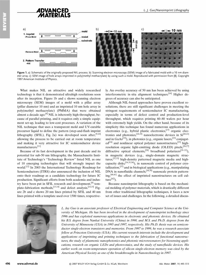
PDMS copolymers that have a sufficiently high siliconecontent provide a very good etching resistance for O2 RIE.This property can be exploited in a double-layer approach tocreate template structures suitable for the lift-off process, asshown in Figure 9a. Figure 9b and c shows the use of the bi-layer resist approach to pattern on top of existing topographyby using PDMS-b-PS and a PMMA undercoating layer. A350 nm linewidth and spacing grating mold was used to im-print and lift-off metal lines. After the first lift-off was com-pleted, the process was repeated in the orthogonal direction.The spin-coated PMMA underlayer served to planarize the
nonflat substrate surface. Figure 9c shows the substrate afterthe deposition of a second metal layer, but before the lift-offprocess. The grid pattern of the combined metal layers is visi-ble in the cross section, above which is the resist mask coveredwith metal. Figure 9d shows a large area of an etched Si holearray obtained by using the fabricated metal grid as a etchmask. Detailed studies of these copolymer systems as nanoim-print resists can be found elsewhere.[72]
3.3.2. Fast Thermally Curable Liquid Resists
The thermal plastic polymers used in NIL become viscousfluids when heated above their Tg values; however, the viscos-ity of heated polymers typically remains high, and thus the im-printing process requires significant pressures. As discussedpreviously these thermoplastic resists normally have a hightendency to stick to the mold, which seriously affects the fidel-ity and quality of the pattern definition. Furthermore, they donot offer the necessary etch resistance. Thermally curablemonomers are an alternative to thermal plastics. These liquidmaterials can be imprinted in a short period of time at lowpressures and temperatures. PDMS-type materials are a classof thermally curable materials widely used by many researchgroups, mainly in the context of soft lithography. In additionto its well-known transparency to UV and visible light alongwith its high biocompatibility, PDMS is a low-surface-energy(19.6 dyn cm–1) material, which allow an easy mold-releasewithout causing any structural damage to the imprinted struc-tures. Moreover, it possesses a very high resistance to oxygenplasma. However, its low Young modulus (ca. 2 MPa for com-mercial Sylgard 184) impedes a good pattern definition at thenanoscale. This can be understood by considering the radiusof curvature (r) of a cured material with a certain modulus(E) and surface energy (c), which can be estimated asr = c/E.[72]. It is easy to see that the low Young modulus ofSylgard PDMS makes it impossible to form nanopatterns withsharp corners. In addition, the low modulus can easily causelateral collapse of the dense imprinted structures when pat-terns are smaller than 500 nm. A higher-modulus (ca. 8 MPa)PDMS (h-PDMS) was developed by Schmith et al. to achievethe patterning of nanoscale structures for soft lithography.Unfortunately, the imprinting cycle (heating–cooling time) forthis h-PDMS was too long (ca. 2 h) for it to be used as animprinting resist material.[73] Following a similar strategy,Malaquin et al. also used a reformulated PDMS (prepolymerwith a smaller chain length) as a thermal-curable resist forNIL.[74] The shorter chain length of the prepolymer utilized inthis formulation provided the stiffness necessary to replicategratings with line widths as small as 200 nm. However, thecrosslinking time was about 60 min at 100 °C and 15 min at150 °C using a printing pressure of 100 MPa; and structureswith an aspect ratio greater than 1 could not be obtainedwhen replicating the 200 nm linewidth structures.[75]
A fast, thermal-curable liquid resist that can be imprintedunder a low pressure with a high precision and throughputwas recently developed in our group.[76] This system is based
Figure 8. a–c) NIL results using a) a 250 nm linewidth PDMS-b-PS grat-ing, b) a silicon nitride mold with 70 nm wide trenches, c) a 70 nm line-wdith grating in PDMS-g-PMIA imprinted using the mold shown in (b).d) Strong light diffraction of an imprinted 200 nm period grating in aPDMS-g-PMIA copolymer on a 4 inch (1 inch = 2.54 cm) wafer immersedin water.
on the same hydrosilylation chemistry of siloxane polymersand consists of four basic chemical components: a vinyl-termi-nated PDMS polymer, a silyl-hydride-based (Si–H) dimethyl-siloxane crosslinker, a platinum catalyst, and an inhibitor. Theinhibitor is an unsaturated organic ester that keeps the cata-lyst inactive until the application of heat, which quickly deac-tivates the inhibitor and releases the catalyst in its active form.The high Si content in this polymer system guarantees thatthe resist has a high etching resistance in RIE processes. Theliquid resist can be spin-coated onto a silicon wafer, forming auniform thin film. The imprinting was done with moderatepressures in the range of 0.2–6.5 MPa at room temperature,and crosslinking was performed at a temperature above 80 °Cwithin a minute. The short time required for curing the materi-al is in sharp contrast with that of commercial PDMS, whichrequires curing for at least tens of minutes and sometimeshours. Also, by changing the molecular weight of the precursorand the percentage of silyl-hydride groups in the crosslinker,the Young modulus of the cured material can be tuned to val-ues several times higher than that of commercial PDMS. Theability to tune the modulus imparts flexibility to the resist to-
wards meeting different process conditions. With the increasedmodulus, structures with feature sizes ranging from severalmicrometers down to 70 nm could be achieved (Fig. 10). Also,by increasing the curing temperature to 120 °C, the materialcan be crosslinked within 10 s because of the rapid deactiva-tion of the inhibitor. This is two orders of magnitude fasterthan previous thermally cured PMDS materials. The fastcrosslinking time satisfies the need for high-speed patterningin practical applications. Importantly, the mold separationdoes not require cooling to room temperature, thereby furtherincreasing the process throughput. Because of the low surfacetension of the patterned film the mold separation is quite easy,even for high-aspect-ratio features. Details of these materialproperties can be found elsewhere.[76] The crosslinked PDMSstructures could also be used as molds for imprinting other re-sist materials or as stamps for microcontact printing, especiallywhen sub-microscale features are desired. For example, earlierwork[76] shows that the replicated PDMS sample can be usedas a stamp to pattern the conductive polymer poly(3,4-ethyl-enedioxythiophene) (PEDOT) with sub-micrometer featuresby using a polymer inking and stamping technique.[19]
Figure 9. a) The O2 RIE resistance of copolymers, in this case PS-PDMS, allows for complex patterning by utilizing a planarization undercoating layer.Undercutting of the planarization layer eases the lift-off process. b) Metal deposition on the double-layer resist. c) Two-layer metal grid deposited bytwo complete NIL steps using a copolymer with a PMMA underlayer. d) Large-area etched Si hole array obtained by using the metal-grid as an etchmask; scale bar: 5 lm.
3.3.3. UV-Curable Liquid Resists for Room-TemperatureNanoimprinting
For certain applications, materials systems that can be UV-cured are preferred over thermally curable systems becausethe heating and cooling cycle of the latter can affect thethroughput, and also have problematic issues that result from athermal-expansion mismatch. The most widely used UV-curingformulations are based on free-radical polymerization ofacrylic and methacrylic monomers because of their high reac-tivity, as used in SFIL.[62] However, such materials systemssuffer from oxygen sensitivity problems: dissolved oxygen sca-venges free radical species, and thus inhibits the polymeriza-tion process at the resist surface at the onset of exposure. Thisprolongs the required exposure time. Oxygen diffusion inambient condition causes a thin perimeter of undercured ma-terial surrounding the mold. Detailed kinetic studies have
been carried out to evaluate the impact of oxygen onSFIL.[77,78] Furthermore, the acrylate-based UV imprint resisthas a large shrinkage upon curing (ca. 10 %), which may affectthe pattern definition or resist adhesion on certain substrates,especially metals and plastics. On the other hand, as pointedout earlier this system does not require a metal catalyst, whichmakes it very attractive to Si-based microelectronics. An alter-native formulation that uses vinyl ether has been investigatedbecause it is based on cationic polymerization and less sensi-tive to oxygen.[79] For the majority of other applications, thedroplet dispensing method used to apply the liquid resist on asubstrate in SFIL significantly limits the throughput of thenanopatterning process. The ability to spin-coat a uniformliquid resist onto a large-area substrate is highly desirable.
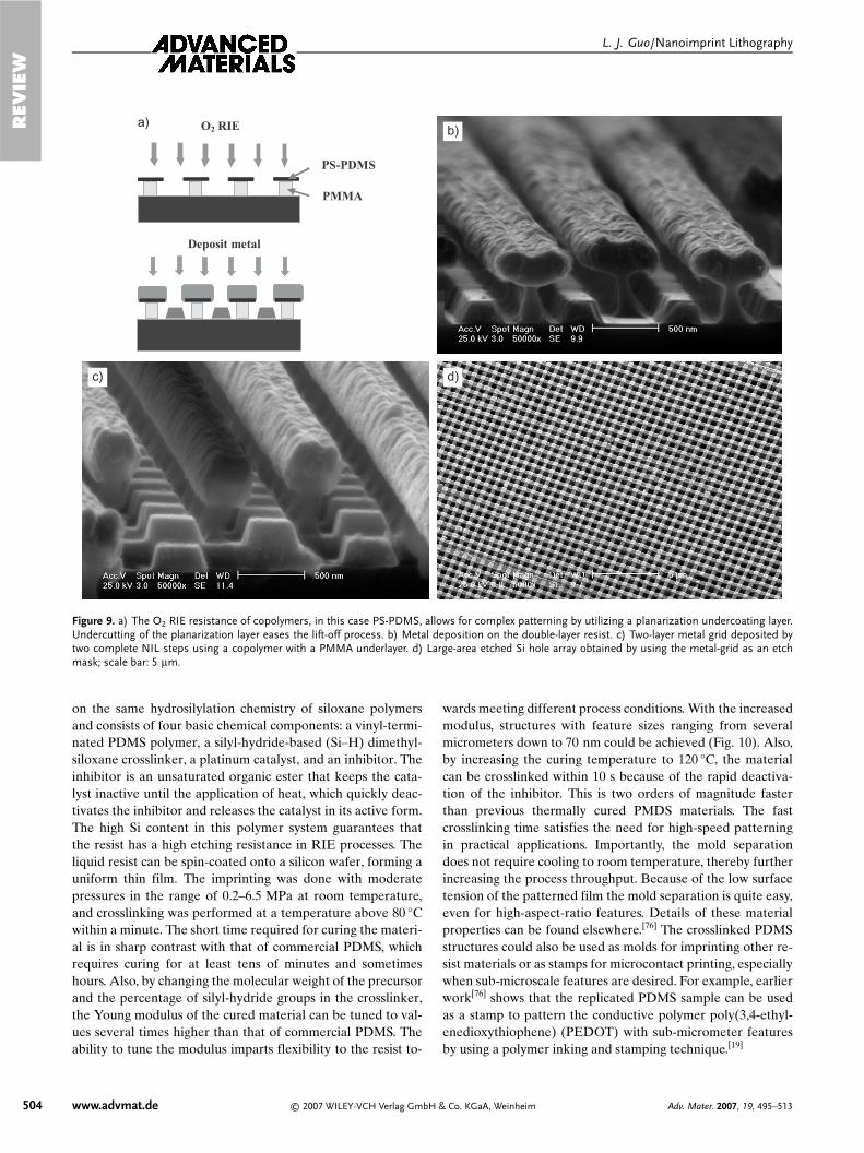
Our group has developed a UV-curable epoxysilicone mate-rial based on the cationic crosslinking of cycloaliphaticepoxies.[52] This resist combines a number of desired featuresfor nanoimprinting. Because cationic polymerization is notprone to oxygen inhibition, as compared to the free radicalpolymerization of acrylate monomers, fewer defects are ex-pected. The resist exhibits a very good dry etching resistancebecause of the high silicon content. Furthermore, its very lowshrinkage after curing (only a fraction of the acrylate system)allows reliable patterning. In addition, with a suitable under-coating polymer a very uniform liquid precursor can beformed simply by spin-coating, which also allows other pro-cesses, such as lift-off, to be easily performed.
The UV-curable liquid resist consists of a silicone-diepoxymonomer, a silicone cross-linking agent, and a photoacid gen-erator. A typical liquid-resist formulation comprises diepoxymonomer (94 %, w/w), crosslinkers (5 %), and a photoacidgenerator (PAG) (1 %). Organic solvents, such as propyleneglycol monomethyl ether acetate (PGMEA), can be used toadjust the viscosity of the resist so that film thicknesses thatrange from one micrometer to 50 nm and below can be read-ily obtained. Although direct spin-coating of this resist onto aSi or oxide substrate causes dewetting of the thin liquid film,as one would expect for a very low viscosity liquid, we foundthat by using a suitable undercoating polymer layer (e.g.,baked PMMA) or a photoresist (SU-8) to provide bettermatching of interfacial energies, stable and uniform liquid thinfilms can be formed on Si or any other substrate. This capabil-ity is critical to imprinting large-area (e.g., wafer-size) samplesin a single step. With such a UV-curable nanoimprint resist,we were able to pattern both micro- and nanoscale structuresat room temperature and at a pressure less than 0.1 MPausing a conventional contact-exposure tool. Figure 11b showsa recessed circular pattern with diameters of 20 lm after im-printing and curing, and Figure 11c and d shows replicatednanoscale patterns, which demonstrates that patterns as smallas 20 nm (limited by the feature resolution on the mold) canbe easily achieved with a conventional contact aligner usingthis resist material. The UV-cured resist has very desirableplasma-etching characteristics, i.e., a very high resistance forO2 plasma etching, making it suitable for use as etch mask forpattern transferring into any underlying organic layers.
Figure 10. a–c) SEM images of imprinted PDMS-type thermally curableliquid resists, showing feature sizes ranging from (several) micrometers(a,b) down to 70 nm (c). Crosslinking by thermal curing can be achievedwithin 10 s.
3.4. Other Imprintable Materials
It should be recognized that NIL can not only be used toform patterns in a polymer resist, but can also be extended tocreate desired structures in many other polymer systems,especially those that have special functionalities, or can beused to form functional polymer device structures directly.Our group has imprinted 2D photonic-crystal nanostructuresin nonlinear optical polymers.[25] Pisignano et al. showed thatconjugated polymers and oligomers can be imprinted at roomtemperature, and that the resulting nanostructures maintainedactive optical properties.[24,80] The mechanism of room-tem-perature NIL was discussed by Lee and co-workers in an ear-lier article, which is based on the compression of free volumeand plastic deformation in thermoplastic materials.[81] Room-temperature processes are highly desirable in patterningorganic semiconductors to avoid oxygen incorporation andsubstitution into conjugated polymers, which occur at hightemperature and can cause irreversible degradation of theiroptical and electrical properties. Li et al. patterned the con-ductive polymer PEDOT for use as electrodes in organic thin-film transistors at high-resolutions.[19] The process is based on
a reverse-imprinting principle and is also carried at room tem-perature to preserve the conductive properties of the materi-al. Recently, we have successfully imprinted a conjugated-polymer-based electron donor layer to form a well-controllednanoscale interface in an organic solar cell in order to im-prove charge separation and power conversion efficiency fororganic photovoltaic applications.[82]
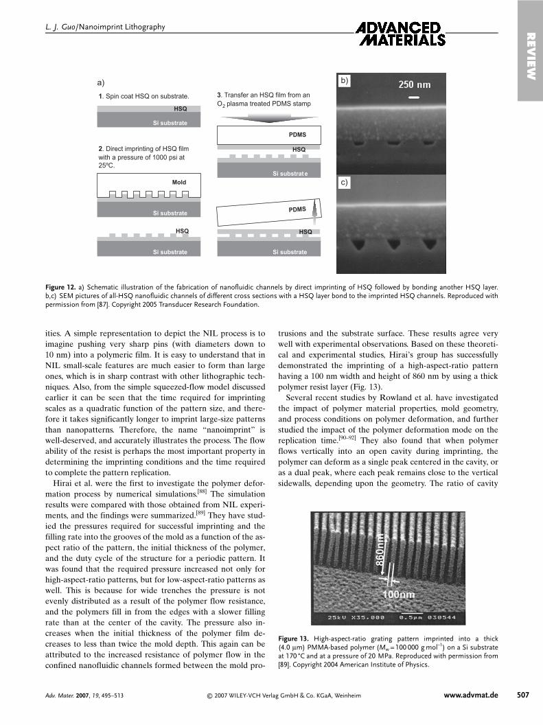
NIL also has many potential applications in microfluidicsand biotechnology. Nielsen et al. demonstrated thermal NILof the cyclic olefin copolymer “Topas”, a thermoplastic mate-rial that is highly UV transparent and chemically resistant tohydrolysis, acids, and organic polar solvents, making it suitablefor lab-on-a-chip applications.[83] Cheng et al. imprinted thefluoropolymer “CYTOP”, a low-k dielectric material that alsopossesses interesting properties regarding the prevention ofprotein absorption. The authors utilized this property to pat-tern the motor proteins and used the imprinted CYTOP nano-structures as physical barriers to guide the motion of microtu-bules with an extremely high efficiency.[84] Biodegradablepolymers are attractive for many biomedical applications,such as DNA and protein analysis chips, as well as for sup-porting structures in tissue engineering. One popular exampleis poly-(L-lactic acid) (PLA) (Tg ≈ 60 °C). Hirai et al. demon-strated imprinting of commercial PLA plastics at 75 °C to pro-duce nanochannels and nanoscale hole arrays.[54] This grouphas also showed imprinting of spin-on-glass for optical appli-cations. Matsui et al. have demonstrated room-temperatureNIL by using another type of spin-on-glass, hydrogen silse-quioxane (HSQ), as the imprint resist material.[85,86] Thepressure needed for these inorganic materials was very high,because of HSQ’s large Young modulus and high viscosity.On the other hand, its hydrophilic surface properties (similarto glass) and the ability to be nanopatterned at room tempera-ture make it an ideal candidate material for creating micro-and nanofluidic applications. We developed a technique toform nanofluidic channels by direct imprinting of hydrophilicHSQ and sealing with another HSQ thin film, with all pro-cessing steps performed near room temperature (Fig. 12). Thewidth of the channels is determined by the mold features, andthe depth can be controlled through the imprinting pressureand time.[87] The capability to produce nanoscale fluidic struc-tures allows fundamental studies of ion or molecule transportin confined spaces. The study of nanofluidics could result inpractical tools for the analysis of biomolecules, such asDNAs[38,39] and proteins.
4. The Nanoimprint Process
4.1. The Cavity-Fill Process
Here, an in-depth look at the imprinting step itself is taken,which is a critical step in the NIL process. To form the desiredpattern, i.e., conforming to the nanoscale protrusion featureson the mold, the resist material underneath the protrusionsmust be displaced and transported to nearby trenches or cav-
Figure 11. a) Structures of monomer and crosslink molecules. b–d) SEMimages of imprinted and UV-cured resist patterns: b) 20 lm diameterrecessed patterns, c) sub-100 nm trench patterns, and d) 20 nmtrenches [52].
ities. A simple representation to depict the NIL process is toimagine pushing very sharp pins (with diameters down to10 nm) into a polymeric film. It is easy to understand that inNIL small-scale features are much easier to form than largeones, which is in sharp contrast with other lithographic tech-niques. Also, from the simple squeezed-flow model discussedearlier it can be seen that the time required for imprintingscales as a quadratic function of the pattern size, and there-fore it takes significantly longer to imprint large-size patternsthan nanopatterns. Therefore, the name “nanoimprint” iswell-deserved, and accurately illustrates the process. The flowability of the resist is perhaps the most important property indetermining the imprinting conditions and the time requiredto complete the pattern replication.
Hirai et al. were the first to investigate the polymer defor-mation process by numerical simulations.[88] The simulationresults were compared with those obtained from NIL experi-ments, and the findings were summarized.[89] They have stud-ied the pressures required for successful imprinting and thefilling rate into the grooves of the mold as a function of the as-pect ratio of the pattern, the initial thickness of the polymer,and the duty cycle of the structure for a periodic pattern. Itwas found that the required pressure increased not only forhigh-aspect-ratio patterns, but for low-aspect-ratio patterns aswell. This is because for wide trenches the pressure is notevenly distributed as a result of the polymer flow resistance,and the polymers fill in from the edges with a slower fillingrate than at the center of the cavity. The pressure also in-creases when the initial thickness of the polymer film de-creases to less than twice the mold depth. This again can beattributed to the increased resistance of polymer flow in theconfined nanofluidic channels formed between the mold pro-
trusions and the substrate surface. These results agree verywell with experimental observations. Based on these theoreti-cal and experimental studies, Hirai’s group has successfullydemonstrated the imprinting of a high-aspect-ratio patternhaving a 100 nm width and height of 860 nm by using a thickpolymer resist layer (Fig. 13).
Several recent studies by Rowland et al. have investigatedthe impact of polymer material properties, mold geometry,and process conditions on polymer deformation, and furtherstudied the impact of the polymer deformation mode on thereplication time.[90–92] They also found that when polymerflows vertically into an open cavity during imprinting, thepolymer can deform as a single peak centered in the cavity, oras a dual peak, where each peak remains close to the verticalsidewalls, depending upon the geometry. The ratio of cavity
Figure 12. a) Schematic illustration of the fabrication of nanofluidic channels by direct imprinting of HSQ followed by bonding another HSQ layer.b,c) SEM pictures of all-HSQ nanofluidic channels of different cross sections with a HSQ layer bond to the imprinted HSQ channels. Reproduced withpermission from [87]. Copyright 2005 Transducer Research Foundation.
Figure 13. High-aspect-ratio grating pattern imprinted into a thick(4.0 lm) PMMA-based polymer (Mw = 100 000 g mol–1) on a Si substrateat 170 °C and at a pressure of 20 MPa. Reproduced with permission from[89]. Copyright 2004 American Institute of Physics.
width to film thickness modulates single versus dual peakcavity filling, regardless of the absolute size of the featuresand the pressure or temperature applied during imprinting. Ingeneral, when the ratio of cavity half width to initial polymerfilm thickness is less than unity, the polymer deforms as asingle peak. For a ratio greater than unity, the polymerdeforms as dual peaks. The cavity is filled fastest for ageometry at the single-peak/dual-peak threshold, with in-creasing fill times for conditions that deviate from this thresh-old, consistent with the findings of Hirai’s group. Figure 14shows simulation results for a polymer filling a cavity duringthermal NIL for three different ratios of cavity size to poly-mer film thickness.[91] For the leftmost and center case of Fig-ure 14, the flow is governed by shear near the mold corners.In both of these cases, there exists a plug of nondeformingpolymer near the center of the cavity. In the case of the right-most geometry, the polymer is squeezed beneath the mold,and this squeezed flow significantly limits the time required tofill this cavity.[92]
The ability to displace a viscous polymer and fill cavitiescan be demonstrated in another example, in which NIL isused to form an optical waveguide directly from a very thinpolymer layer. The device is a polymer-based optical micro-ring resonator,[68] which can find applications in optical com-munication, label-free biosensing,[93] and high-frequencyultrasound detection.[94] In this process an inverse pattern ofthe waveguide and the microring is fabricated as a mold, hav-ing a depth of ca. 2 lm (Fig. 15a). For the NIL process, only athin polymer layer with an initial thickness in the range of200–300 nm is spin-coated, but the final waveguide thicknessreaches ca. 2 lm (Fig. 15b). This implies that the amount ofpolymer being displaced and transported to the mold trench isquite significant. Such a mode of imprinting is very differentfrom that typically used in NIL, where nanoscale mold protru-sions are imprinted into a polymer resist. Accordingly, theconditions for imprinting need to be modified by using a high-
er pressure and longer imprinting time to assist the polymerflow.[68]
Finally, Yu et al. developed a technique based on time-re-solved scatterometry to perform in situ real-time monitoringof the cavity-filling process in NIL.[95] In this approach, theauthors used a surface relief grating structure as the imprint-ing mold, and monitored the diffracted light continuously asthe mold penetrated into the polymer resist. The resultsmatched the simulation very well, indicating that this tech-nique is a powerful tool for in situ NIL process control.
5. Variations of NIL Processess
In recent years various new approaches aimed at enhancingthe capability of NIL have been studied. Roller NIL was pro-posed to provide better uniformity and decrease the printingforce, and demonstrated sub-100 nm feature transfer by usinga hard mold.[96] The rigiflex mold was developed to provide abetter conformal contact with the substrate and to reduce thepressure required during imprint.[43] This approach can alsobe extended for roll-to-roll imprinting of nanostructures. In
Figure 14. Simulations showing the temporal evolution of polymer flow into an imprint mold cavity for three different ratios of polymer cavity size topolymer thickness. In general, the ratio of cavity half width to polymer film thickness determines whether a single peak or dual peak will occur for thepolymer deformation. The polymer gray scale indicates shear: a darker color represents higher shear. The location of polymer shear modulates the poly-mer deformation mode, which in turn modulates the cavity-filling time. Reproduced with permission from [90]. Copyright 2004 Institute of Physics.
a) b)
Figure 15. SEM images showing perspective view of a) a mold used toimprint the coupled polymer waveguides; scale bar: 1 lm and b) an im-printed polymer microring resonator device; scale bar: 10 lm (The insertshows a cross section of the waveguide after an undercutting wet etch).
SFIL, a reverse-tone bilayerapproach was developed toenhance the reliability in fabri-cating high-aspect-ratio struc-tures.[97]
5.1. Reverse-Nanoimprinting
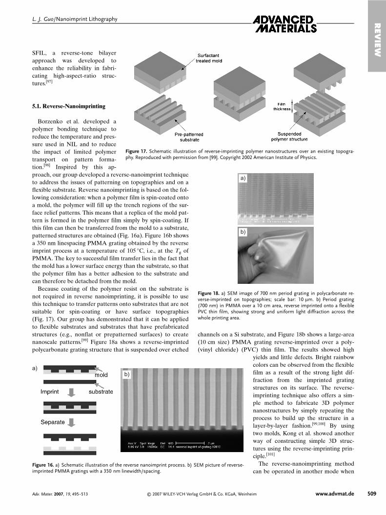
Borzenko et al. developed apolymer bonding technique toreduce the temperature and pres-sure used in NIL and to reducethe impact of limited polymertransport on pattern forma-tion.[98] Inspired by this ap-proach, our group developed a reverse-nanoimprint techniqueto address the issues of patterning on topographies and on aflexible substrate. Reverse nanoimprinting is based on the fol-lowing consideration: when a polymer film is spin-coated ontoa mold, the polymer will fill up the trench regions of the sur-face relief patterns. This means that a replica of the mold pat-tern is formed in the polymer film simply by spin-coating. Ifthis film can then be transferred from the mold to a substrate,patterned structures are obtained (Fig. 16a). Figure 16b showsa 350 nm linespacing PMMA grating obtained by the reverseimprint process at a temperature of 105 °C, i.e., at the Tg ofPMMA. The key to successful film transfer lies in the fact thatthe mold has a lower surface energy than the substrate, so thatthe polymer film has a better adhesion to the substrate andcan therefore be detached from the mold.
Because coating of the polymer resist on the substrate isnot required in reverse nanoimprinting, it is possible to usethis technique to transfer patterns onto substrates that are notsuitable for spin-coating or have surface topographies(Fig. 17). Our group has demonstrated that it can be appliedto flexible substrates and substrates that have prefabricatedstructures (e.g., nonflat or prepatterned surfaces) to createnanoscale patterns.[99] Figure 18a shows a reverse-imprintedpolycarbonate grating structure that is suspended over etched
channels on a Si substrate, and Figure 18b shows a large-area(10 cm size) PMMA grating reverse-imprinted over a poly-(vinyl chloride) (PVC) thin film. The results showed high
yields and little defects. Bright rainbowcolors can be observed from the flexiblefilm as a result of the strong light dif-fraction from the imprinted gratingstructures on its surface. The reverse-imprinting technique also offers a sim-ple method to fabricate 3D polymernanostructures by simply repeating theprocess to build up the structure in alayer-by-layer fashion.[99,100] By usingtwo molds, Kong et al. showed anotherway of constructing simple 3D struc-tures using the reverse-imprinting prin-ciple.[101]
The reverse-nanoimprinting methodcan be operated in another mode when
Figure 16. a) Schematic illustration of the reverse nanoimprint process. b) SEM picture of reverse-imprinted PMMA gratings with a 350 nm linewidth/spacing.
Figure 17. Schematic illustration of reverse-imprinting polymer nanostructures over an existing topogra-phy. Reproduced with permission from [99]. Copyright 2002 American Institute of Physics.
a)
b)
Figure 18. a) SEM image of 700 nm period grating in polycarbonate re-verse-imprinted on topographies; scale bar: 10 lm. b) Period grating(700 nm) in PMMA over a 10 cm area, reverse imprinted onto a flexiblePVC thin film, showing strong and uniform light diffraction across thewhole printing area.
the depth of the mold feature is large compared to the coatedpolymer film. In this case, the coated polymer can not planar-ize the relief features on the mold surface, and when pressedagainst a substrate only the protrusion features on top of themold are transferred to the substrate material.[102,103] This issimilar to the inking process, but the stamp has nanoscale sur-face relief features. The polymer inking method is essentiallyan additive patterning technique that does not require furtherprocessing steps. This feature is very attractive for patterningpolymers with special functionalities that are sensitive tochemical or plasma processing. Such examples include con-ductive polymers and conjugated organic materials. Recently,the conductive polymer PEDOT has been patterned by thepolymer inking technique to function as electrodes for organicelectronic applications.[19] Lee et al. demonstrated the pat-terning of a bilayer of metal and polymer.[104]
5.2. Combined Nanoimprint-and-Photolithography
NIL works effectively for nanoscale features, but experi-ences difficulties when replicating larger features. On theother hand, a general lithographic technique should be capa-ble of producing both large and small features in various com-binations and with various pattern densities. Previous studieshave shown that defects or even pattern failures in the formof incomplete pattern transfer can occur as a result of the highviscosity of the polymer melt and the varied pattern densitieson the mold.[105] A mix-and-match lithography approach thatuses two separate lithography steps has been proposed to ad-dress this problem,[106] at the expense of an increased com-plexity and number of processing steps as well as the require-ment of pattern registration between the two separate steps.Our group developed a technique to solve this problem by in-troducing a hybrid mask concept and combining NIL withphotolithography (CNP).[107] As shown in Figure 19a, the hy-brid mold is made of a UV-transparent material and acts asboth an NIL mold and as a photolithography mask. Protru-sions are made on the mold for imprinting nanoscale features,while metal pads are embedded into the mold and serve as aphotolithography metal mask to replicate the large patterns.Detailed fabrication procedures have been reported else-where.[108] In the CNP process, the hybrid mold is first im-printed into the resist layer by pressure, and subsequently theentire mold–substrate assembly is exposed to UV radiation.After the hybrid mold and the substrate are separated, thesubstrate is immersed in a developer solution to remove unex-posed resist (i.e., resist that was blocked by the metal pads).After development, both large and nanoscale patterns are cre-ated in the polymer resist in one step. The authors have dem-onstrated the effectiveness of this technique by using a nega-tive-tone photoresist, and have also fabricated nanoelectrodestructures with drastically different length scales, from 150 lm
down to tens of nanometers (Fig. 19b). Such structures wereused in making nanoscale organic thin-film transistors.[108]
The CNP process offers several advantages: First, the nano-scale protrusion features on the hybrid mold only need todisplace a very small amount of polymer, which ensures alow-pressure process. Second, by forming the large patterns asa photomask (i.e., making them as metal pads), the residuelayer thickness distribution is simplified, which can ease theresidue removal step significantly. Third, as a further improve-ment, if the metal mask used for etching the mold is left ontop of the mold protrusions it can prevent the exposure of theresist layer underneath. The unexposed residual layer can beremoved in a developer solution without additional O2 dryetching steps.[107] In this manner it is possible to eliminate theseparate residual removal step in NIL completely, and simul-taneously the nonuniform residual layer thickness problemcould be solved altogether. In addition, the metal layer on thehybrid mold used in CNP serves as better registration marks,as compared with the relief structures used in SFIL or NIL.Because the latter can not create a sufficient refractive-indexcontrast upon intimate contact with a polymer layer that hasan index close to the silica or quartz mold, registrationbetween different lithography layers is difficult. To take ad-vantage of the high-contrast alignment marks in CNP, one candesign grating patterns on the mold and on substrate and usethe Moiré interference technique to achieve a high-accuracyalignment.
6. Conclusion
The nanoimprint technique has enabled parallel nanoscalepatterning with ultrahigh resolutions. The simplicity of thismethod has made it appealing to researchers in various fields.Hopefully, this Review will provide the readers with an over-view of some aspects of the rapid developments in the field ofnanoimprint technology in recent years, especially where newmaterials are concerned, but it is by no means meant to be ex-haustive. Novel techniques based on the concept of mechani-cal printing or embossing are appearing rapidly. New varia-tions of the technique, aimed at different applications, havealso been developed at a fast pace. It is certain that advancesin (new) imprinting materials will fuel further developmentsin this field. One exciting opportunity is the development oftruly continuous roll-to-roll imprinting of nanostructures,which could provide unprecedented throughput for manypractical applications. Hopefully, more researchers will be in-spired to explore these techniques, and to exploit many newpossibilities in the future.
–[1] Y. Xia, G. M. Whitesides, Polym. Mater. Sci. Eng. 1997, 77, 596.[2] S. Y. Chou, P. R. Krauss, P. J. Renstrom, Appl. Phys. Lett. 1995, 67,
3114.[3] S. C. Minne, P. Flueckiger, H. T. Soh, C. F. Quate, J. Vac. Sci. Tech-
nol. B 1995, 13, 1380.[4] R. D. Piner, J. Zhu, F. Xu, S. Hong, C. A. Mirkin, Science 1999, 283,
661.[5] B. D. Gates, Q. B. Xu, M. Stewart, D. Ryan, C. G. Willson, G. M.
Whitesides, Chem. Rev. 2005, 105, 1171.[6] L. J. Guo, J. Phys. D 2004, 37, R123.[7] S. Y. Chou, P. R. Krauss, P. J. Renstrom, Science 1996, 272, 85.[8] S. Y. Chou, P. R. Krauss, W. Zhang, L. J. Guo, L. Zhuang, J. Vac. Sci.
Technol. B 1997, 15, 2897.[9] P. Ruchhoeft, M. Colburn, B. Choi, H. Nounu, S. Johnson, T. Bailey,
S. Damle, M. Stewart, J. Ekerdt, S. V. Sreenivasan, J. C. Wolfe, C. G.Willson, J. Vac. Sci. Technol. B 1999, 17, 2965.
[10] M. D. Stewart, S. C. Johnson, S. V. Sreenivasan, D. J. Resnick, C. G.Willson, J. Microlithogr., Microfabr., Microsyst. 2005, 4, 011 002.
[11] D. J. Resnick, W. J. Dauksher, D. Mancini, K. J. Nordquist, T. C.Bailey, S. Johnson, N. Stacey, J. G. Ekerdt, C. G. Willson, S. V. Sree-nivasan, N. Schumaker, J. Vac. Sci. Technol. B 2003, 21, 2624.
[12] Special Report, Technol. Rev. 2003, 106, 36.[13] T. C. Bailey, D. J. Resnick, D. Mancini, K. J. Nordquist, W. J.
Dauksher, E. Ainley, A. Talin, K. Gehoski, J. H. Baker, B. J. Choi,S. Johnson, M. Colburn, M. Meissl, S. V. Sreenivasan, J. G. Ekerdt,C. G. Willson, Microelectron. Eng. 2002, 61-2, 461.
[14] W. J. Dauksher, K. J. Nordquist, D. P. Mancini, D. J. Resnick, J. H.Baker, A. E. Hooper, A. A. Talin, T. C. Bailey, A. M. Lemonds,S. V. Sreenivasan, J. G. Ekerdt, C. G. Willson, J. Vac. Sci. Technol. B2002, 20, 2857.
[15] T. Bailey, B. J. Choi, M. Colburn, M. Meissl, S. Shaya, J. G. Ekerdt,S. V. Sreenivasan, C. G. Willson, J. Vac. Sci. Technol. B 2000, 18,3572.
Figure 19. a) Schematic illustration of the CNP technique, using a hybrid mask mold for one-step lithography of both large and nanopatterns. Repro-duced with permission from [107]. Copyright 2004 Elsevier. b) SEM images of a finger-shaped nanoelectrode with large metal pads patterned by theCNP approach. Reproduced with permission from [108]. Copyright 2006 Institute of Physics.
[16] A. Fuchs, B. Vratzov, T. Wahlbrink, Y. Georgiev, H. Kurz, J. Vac. Sci.Technol. B 2004, 22, 3242.
[17] M. C. McAlpine, R. S. Friedman, D. M. Lieber, Nano Lett. 2003, 3,443.
[18] C. C. Cedeno, J. Seekamp, A. P. Kam, T. Hoffmann, S. Zankovych,C. M. S. Torres, C. Menozzi, M. Cavallini, M. Murgia, G. Ruani,F. Biscarini, M. Behl, R. Zentel, J. Ahopelto, Microelectron. Eng.2002, 61-2, 25.
[19] D. Li, L. J. Guo, Appl. Phys. Lett. 2006, 88, 63 513.[20] L. J. Guo, P. R. Krauss, S. Y. Chou, Appl. Phys. Lett. 1997, 71, 1881.[21] W. Zhang, S. Y. Chou, Appl. Phys. Lett. 2003, 83, 1632.[22] D. S. Macintyre, Y. Chen, D. Gourlay, E. Boyd, D. Moran, X. Cao,
K. Elgaid, C. R. Stanley, I. Thayne, S. Thoms, J. Vac. Sci. Technol. B2003, 21, 2783.
[23] D. Pisignano, L. Persano, E. Mele, P. Visconti, M. Anni, G. Gigli,R. Cingolani, L. Favaretto, G. Barbarella, Synth. Met. 2005, 153, 237.
[24] D. Pisignano, L. Persano, M. F. Raganato, P. Visconti, R. Cingolani,G. Barbarella, L. Favaretto, G. Gigli, Adv. Mater. 2004, 16, 525.
[25] L. J. Guo, X. Cheng, C. Y. Chao, J. Mod. Opt. 2002, 49, 663.[26] X. Cheng, Y. T. Hong, J. Kanicki, L. J. Guo, J. Vac. Sci. Technol. B
2002, 20, 2877.[27] P. C. Kao, S. Y. Chu, T. Y. Chen, C. Y. Zhan, F. C. Hong, C. Y.
Chang, L. C. Hsu, W. C. Liao, M. H. Hon, IEEE Trans. Electron De-vices 2005, 52, 1722.
[28] J. Wang, H. Kostal, Laser Focus World 2005, 41, 76.[29] J. J. Wang, W. Zhang, X. G. Deng, J. D. Deng, F. Liu, P. Sciortino,
L. Chen, Opt. Lett. 2005, 30, 195.[30] S. W. Ahn, K. D. Lee, J. S. Kim, S. H. Kim, J. D. Park, S. H. Lee,
P. W. Yoon, Nanotechnology 2005, 16, 1874.[31] Y. Ekinci, H. H. Solak, C. David, H. Sigg, Opt. Express 2006, 14,
2323.[32] S. Y. Chou, Proc. IEEE 1997, 85, 652.[33] W. Wu, B. Cui, X. Y. Sun, W. Zhang, L. Zhuang, L. S. Kong, S. Y.
Chou, J. Vac. Sci. Technol. B 1998, 16, 3825.[34] J. I. Martin, J. Nogues, K. Liu, J. L. Vicent, I. K. Schuller, J. Magn.
Magn. Mater. 2003, 256, 449.[35] T. Glinsner, P. Hangweier, H. Luesebrink, P. Dorsey, A. Homola,
D. Wachenschwanz, Solid State Technol. 2005, 48, 51.[36] G. M. McClelland, M. W. Hart, C. T. Rettner, M. E. Best, K. R. Car-
ter, B. D. Terris, Appl. Phys. Lett. 2002, 81, 1483.[37] Z. J. Hu, G. Baralia, V. Bayot, J. F. Gohy, A. M. Jonas, Nano Lett.
2005, 5, 1738.[38] H. Cao, Z. N. Yu, J. Wang, J. O. Tegenfeldt, R. H. Austin, E. Chen,
W. Wu, S. Y. Chou, Appl. Phys. Lett. 2002, 81, 174.[39] L. J. Guo, X. Cheng, C. F. Chou, Nano Lett. 2004, 4, 69.[40] J. D. Hoff, L. J. Cheng, E. Meyhofer, L. J. Guo, A. J. Hunt, Nano
Lett. 2004, 4, 853.[41] D. Falconnet, D. Pasqui, S. Park, R. Eckert, H. Schift, J. Gobrecht,
R. Barbucci, M. Textor, Nano Lett. 2004, 4, 1909.[42] W. Hu, E. K. F. Yim, R. M. Reano, K. W. Leong, S. W. Pang, J. Vac.
Sci. Technol. B 2005, 23, 2984.[43] D. Suh, S.-J. Choi, H. H. Lee, Adv. Mater. 2005, 17, 1554.[44] D. Y. Khang, H. Yoon, H. H. Lee, Adv. Mater. 2001, 13, 749.[45] B. D. Lucas, J. Kim, L. J. Guo, unpublished.[46] M. D. Austin, H. X. Ge, W. Wu, M. T. Li, Z. N. Yu, D. Wasserman,
S. A. Lyon, S. Y. Chou, Appl. Phys. Lett. 2004, 84, 5299.[47] M. Tormen, A. Carpentiero, L. Vaccari, M. Altissimo, E. Ferrari,
D. Cojoc, E. Di Fabrizio, J. Vac. Sci. Technol. B 2005, 23, 2920.[48] G. Y. Jung, Z. Y. Li, W. Wu, Y. Chen, D. L. Olynick, S. Y. Wang,
W. M. Tong, R. S. Williams, Langmuir 2005, 21, 1158.[49] H. Schift, S. Saxer, S. Park, C. Padeste, U. Pieles, J. Gobrecht, Nano-
technology 2005, 16, S171.[50] D. Y. Khang, H. H. Lee, Langmuir 2004, 20, 2445.[51] D. Y. Khang, H. Kang, T. Kim, H. H. Lee, Nano Lett. 2004, 4, 633.[52] X. Cheng, L. J. Guo, P. F. Fu, Adv. Mater. 2005, 17, 1419.
[53] D. G. Choi, J. H. Jeong, Y. S. Sim, E. S. Lee, W. S. Kim, B. S. Bae,Langmuir 2005, 21, 9390.
[54] Y. Hirai, Y. Tanaka, J. Photopolym. Sci. Technol. 2002, 15, 475.[55] Y. Hirai, J. Photopolym. Sci. Technol. 2005, 18, 551.[56] Alternative Lithography: Unleashing the Potentials of Nanotechnol-
ogy (Ed: C. M. Sotomayor-Torres), Kluwer Academic/Plenum, NewYork 2003, pp. 36–41.
[57] L. Wu, S. Y. Chou, in Technical Digest of 47th EIPBN Conf. 2003,Tampa, FL 2003, 293.
[58] H. C. Scheer, N. Bogdanski, M. Wissen, T. Konishi, Y. Hirai, J. Vac.Sci. Technol. B 2005, 23, 2963.
[59] G. Y. Jung, S. Ganapathiappan, X. Li, D. A. A. Ohlberg, D. L. Oly-nick, Y. Chen, W. M. Tong, R. S. Williams, Appl. Phys. A 2004, 78,1169.
[60] D. Y. Khang, H. H. Lee, Appl. Phys. Lett. 2000, 76, 870.[61] Y. Hirai, S. Yoshida, N. Takagi, J. Vac. Sci. Technol. B 2003, 21, 2765.[62] M. Colburn, S. Johnson, M. Stewart, S. Damle, T. Bailey, B. Choi,
M. Wedlake, T. Michaelson, S. Sreenivasan, J. Ekerdt, Proc. SPIE-Int. Soc. Opt. Eng. 1999, 3676, 379.
[63] H. Schulz, D. Lyebyedyev, H. C. Scheer, K. Pfeiffer, G. Bleidiessel,G. Grutzner, J. Ahopelto, J. Vac. Sci. Technol. B 2000, 18, 3582.
[64] K. Pfeiffer, F. Reuther, M. Fink, G. Gruetzner, P. Carlberg,I. Maximov, L. Montelius, J. Seekamp, S. Zankovych, C. M. Soto-mayor-Torres, H. Schulz, H. C. Scheer, Microelectron. Eng. 2003,67–68, 266.
[65] M. D. Stewart, C. G. Willson, MRS Bull. 2005, 30, 947.[66] F. Reuther, J. Photopolym. Sci. Technol. 2005, 18, 525.[67] N. Sakai, J. Taniguchi, K. Kawaguchi, M. Ohtaguchi, T. Hirasawa,
J. Photopolym. Sci. Technol. 2005, 18, 531.[68] C. Y. Chao, L. J. Guo, J. Vac. Sci. Technol. B 2002, 20, 2862.[69] M. Beck, M. Graczyk, I. Maximov, E. L. Sarwe, T. G. I. Ling,
M. Keil, L. Montelius, Microelectron. Eng. 2002, 61-2, 441.[70] P. Fu, M. K. Tomalia, Macromolecules 2004, 37, 267.[71] P. Choi, P. Fu, L. J. Guo, Adv. Funct. Mater., doi: 10.1002/
adfm.200600257.[72] C. Y. Hui, A. Jagota, Y. Y. Lin, E. J. Kramer, Langmuir 2002, 18,
1394.[73] H. Schmid, B. Michel, Macromolecules 2000, 33, 3042.[74] L. Malaquin, F. Carcenac, C. Vieu, M. Mauzac, Microelectron. Eng.
2002, 61-2, 379.[75] L. Malaquin, C. Vieu, in Alternative Lithography (Ed: C. M. Soto-
mayor-Torres) Kluwer Academic/Plenum, New York 2003, pp. 169–203.
[76] C. Pina-Hernandez, J.-S. Kim, L. J. Guo, P.-F. Fu, Adv. Mater. 2006,in press.
[77] M. D. Dickey, R. L. Burns, E. K. Kim, S. C. Johnson, N. A. Stacey,C. G. Willson, AIChE J. 2005, 51, 2547.
[78] M. D. Dickey, C. G. Willson, AIChE J. 2006, 52, 777.[79] E. K. Kim, M. D. Stewart, K. Wu, F. L. Palmieri, M. D. Dickey, J. G.
Ekerdt, C. G. Willson, J. Vac. Sci. Technol. B 2005, 23, 2967.[80] E. Mele, F. Di Benedetto, L. Persano, R. Cingolani, D. Pisignano,
Nano Lett. 2005, 5, 1915.[81] D. Y. Khang, H. Yoon, H. H. Lee, Adv. Mater. 2001, 13, 749.[82] M. S. Kim, J. S. Kim, J. Cho, M. Shtein, L. J. Guo, J. Kim, unpub-
lished.[83] T. Nielsen, D. Nilsson, F. Bundgaard, P. Shi, P. Szabo, O. Geschke,
A. Kristensen, J. Vac. Sci. Technol. B 2004, 22, 1770.[84] L. J. Cheng, M. T. Kao, E. Meyhçfer, L. J. Guo, Small 2005, 1, 409.[85] Y. Igaku, S. Matsui, H. Ishigaki, J. Fujita, M. Ishida, Y. Ochiai,
H. Namatsu, M. Komuro, H. Hiroshima, Jpn. J. Appl. Phys. Part 12002, 41, 4198.
[86] S. Matsui, Y. Igaku, H. Ishigaki, J. Fujita, M. Ishida, Y. Ochiai,H. Namatsu, M. Komuro, J. Vac. Sci. Technol. B 2003, 21, 688.
[87] L. Cheng, S. Chang, L. J. Guo, in Proc. MicroTAS 2005, TransducerResearch Foundation, Boston, MA 2005, 518.
[88] Y. Hirai, M. Fujiwara, T. Okuno, Y. Tanaka, M. Endo, S. Irie, K. Na-kagawa, M. Sasago, J. Vac. Sci. Technol. B 2001, 19, 2811.
[89] Y. Hirai, T. Konishi, T. Yoshikawa, S. Yoshida, J. Vac. Sci. Technol. B2004, 22, 3288.
[90] H. D. Rowland, W. P. King, J. Micromech. Microeng. 2004, 14, 1625.[91] H. D. Rowland, A. C. Sun, P. R. Schunk, W. P. King, J. Micromech.
Microeng. 2005, 15, 2414.[92] H. D. Rowland, W. P. King, A. C. Sun, P. R. Schunk, J. Vac. Sci.
Technol. B 2005, 23, 2958.[93] C. Y. Chao, W. Fung, L. J. Guo, IEEE J. Sel. Top. Quantum Electron.
2006, 12, 134.[94] S. Ashkenazi, C. Y. Chao, L. J. Guo, M. O’Donnell, Appl. Phys. Lett.
2004, 85, 5418.[95] Z. N. Yu, H. Gao, S. Y. Chou, Appl. Phys. Lett. 2004, 85, 4166.[96] H. Tan, A. Gilbertson, S. Y. Chou, J. Vac. Sci. Technol. B 1998, 16,
3926.[97] S. V. Sreenivasan, A. McMackin, F. Xu, D. Wang, N. Stacey, Micro
2005, 23, 37.[98] T. Borzenko, M. Tormen, G. Schmidt, L. W. Molenkamp, H. Janssen,
Appl. Phys. Lett. 2001, 79, 2246.
[99] L.-R. Bao, X. Cheng, X. D. Huang, L. J. Guo, S. W. Pang, A. F. Yee,J. Vac. Sci. Technol. B 2002, 20, 2881.
[100] N. Kehagias, M. Zelsmann, C. M. S. Torres, K. Pfeiffer, G. Ahrens,G. Gruetzner, J. Vac. Sci. Technol. B 2005, 23, 2954.
[101] Y. P. Kong, H. Y. Low, S. W. Pang, A. F. Yee, J. Vac. Sci. Technol. B2004, 22, 3251.
[102] X. D. Huang, L. R. Bao, X. Cheng, L. J. Guo, S. W. Pang, A. F. Yee,J. Vac. Sci. Technol. B 2002, 20, 2872.
[103] L. Tan, Y. P. Kong, S. W. Pang, A. F. Yee, J. Vac. Sci. Technol. B2004, 22, 2486.
[104] D. Suh, J. Rhee, H. H. Lee, Nanotechnology 2004, 15, 1103.[105] H. C. Scheer, H. Schulz, Microelectron. Eng. 2001, 56, 311.[106] K. Pfeiffer, A. Fink, G. Gruetzner, G. Bleidiessel, H. Schulz,
H. Scheer, Microelectron. Eng. 2001, 57–8, 381.[107] a) X. Cheng, L. J. Guo, Microelectron. Eng. 2004, 71, 288.
b) X. Cheng, L. J. Guo, Microelectron. Eng. 2004, 71, 277.[108] X. Cheng, D. W. Li, L. J. Guo, Nanotechnology 2006, 17, 927.