25
Nanometer Testing: Challenges and Solutions Jais Abraham AMD India Design Centre
Nanometer Testing: Challenges and Solutions
Jais Abraham AMD India Design Centre
Characteristics of Nanometer Devices
Design trendsIncreasing corners of operation (multiple frequencies, voltage, power scenarios)Increasing integration (SOCs, SIPs)Permeation of high bandwidth serial/ differential interfaces
Process issuesProcess variations becoming key concernIncreasing wiring densities leading to complex signal integrity problemsDominance of new kinds of defects based on the metal subsystem
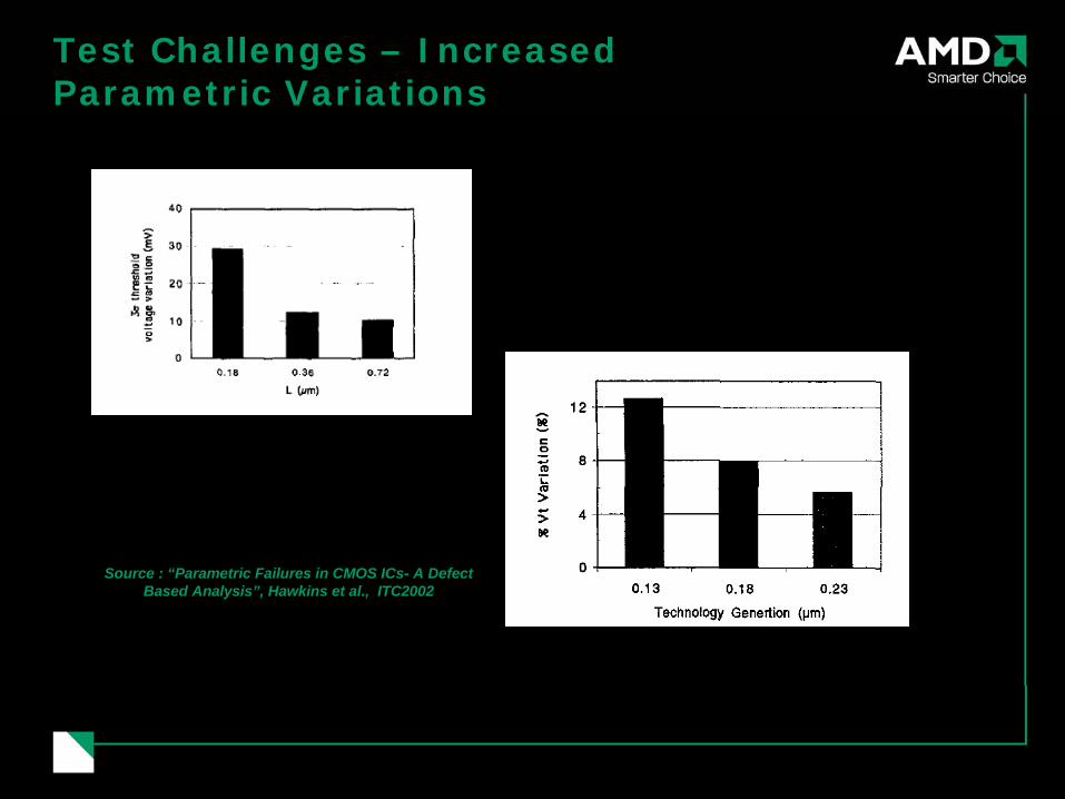
Test Challenges – Increased Parametric Variations
Source : “Parametric Failures in CMOS ICs- A Defect Based Analysis”, Hawkins et al., ITC2002
Cur
rent
Speed
Current vs. Speed Limit
e- e-e- e-e- e-
L TARGET
L EFFECTIVE
L EFFECTIVE = L TARGET - X
e- e-e- e-e- e-
L TARGET
L EFFECTIVE
e- e-e- e-e- e-
L TARGET
L EFFECTIVE
L EFFECTIVE = L TARGET - X
X : Lot1O : Lot2
Minor bridging defects etc.Minor bridging defects etc.
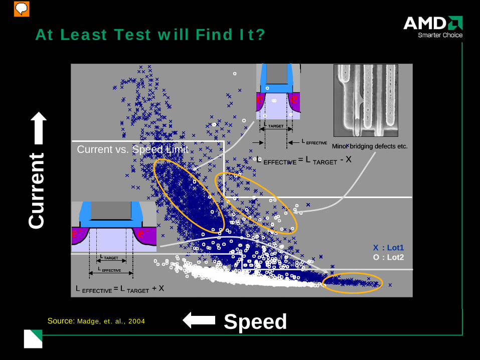
At Least Test will Find It?
e - e -e - e -e - e -
L TARGET
L EFFECTIVE
L EFFECTIVE = L TARGET + X
e - e -e - e -e - e -
L TARGET
L EFFECTIVE
e - e -e - e -e - e -
L TARGET
L EFFECTIVE
L EFFECTIVE = L TARGET + X
Source: Madge, et. al., 2004
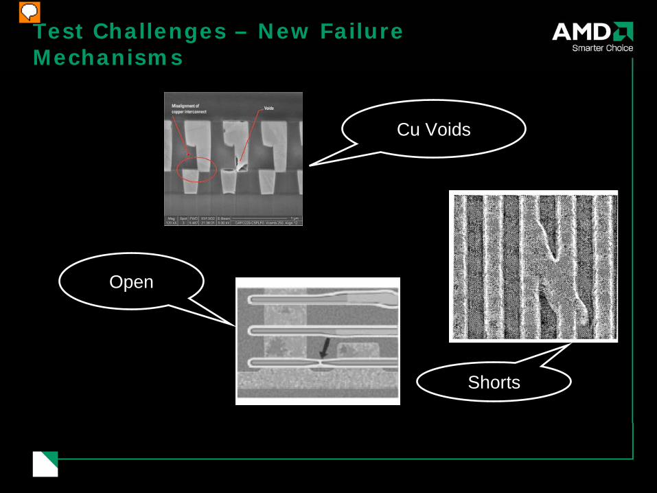
Test Challenges – New Failure Mechanisms
Cu Voids
Open
Shorts
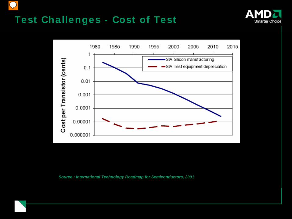
Test Challenges - Cost of Test
Source : International Technology Roadmap for Semiconductors, 2001
Test Challenges – Power
Test power could be more than functional power– more regions of the device operating than in functional mode
– switching of logic during scan shift
With increasing design frequencies & integration– Can the tester supply the power required in the test mode
– Can the package support the power required in the test mode
– Will the part be able to withstand the power consumption during high voltage testing
Test Challenges - Yield Learning
Defect sizes scale as quickly or faster than the device features
Difficulty in localizing faults increases one order of magnitudeevery six years
Defective chips offer significant information on these failure mechanisms
Yield learning is becoming increasingly important
To tune the manufacturing processes to achieve higher profits
To reduce the time for volume production since product life cycles are coming down
SOLUTIONS
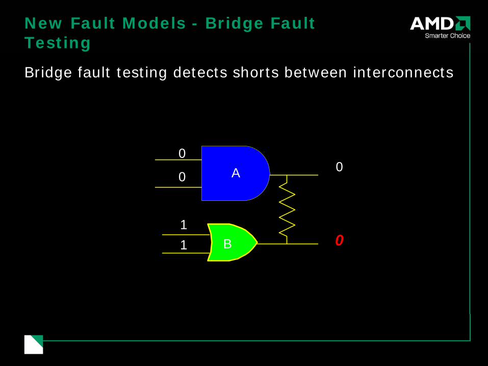
New Fault Models - Bridge Fault Testing
Bridge fault testing detects shorts between interconnects
0
0
11
0
0B
A
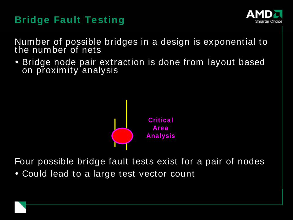
Bridge Fault Testing
Number of possible bridges in a design is exponential to the number of nets
Bridge node pair extraction is done from layout based on proximity analysis
Four possible bridge fault tests exist for a pair of nodesCould lead to a large test vector count
CriticalArea
Analysis
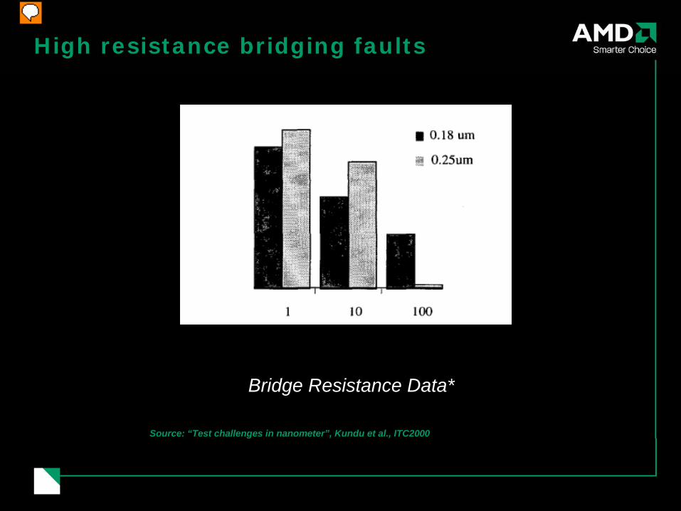
High resistance bridging faults
Bridge Resistance Data*
Source: “Test challenges in nanometer”, Kundu et al., ITC2000
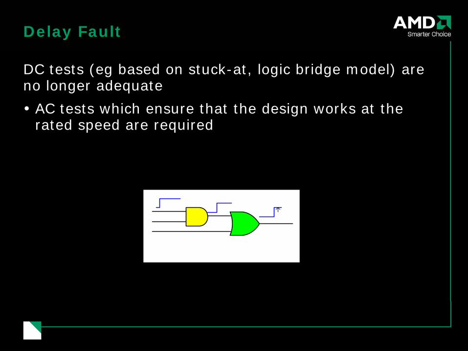
Delay Fault
DC tests (eg based on stuck-at, logic bridge model) are no longer adequate
AC tests which ensure that the design works at the rated speed are required
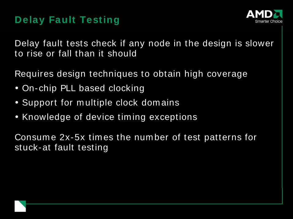
Delay Fault Testing
Delay fault tests check if any node in the design is slower to rise or fall than it should
Requires design techniques to obtain high coverage
On-chip PLL based clocking
Support for multiple clock domains
Knowledge of device timing exceptions
Consume 2x-5x times the number of test patterns for stuck-at fault testing
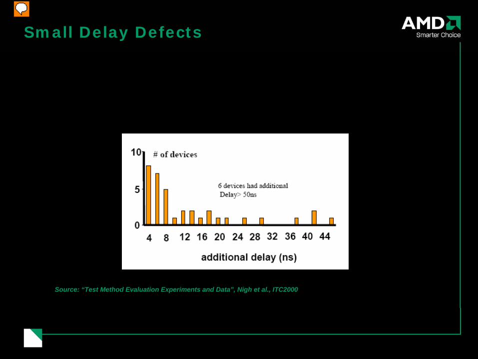
Small Delay Defects
Source: “Test Method Evaluation Experiments and Data”, Nigh et al., ITC2000
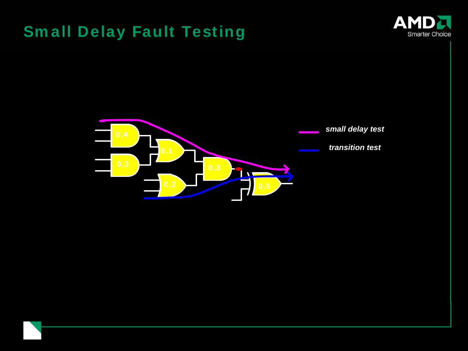
Small Delay Fault Testing
0.4
0.30.1
0.2
0.3
0.5
small delay test
transition test
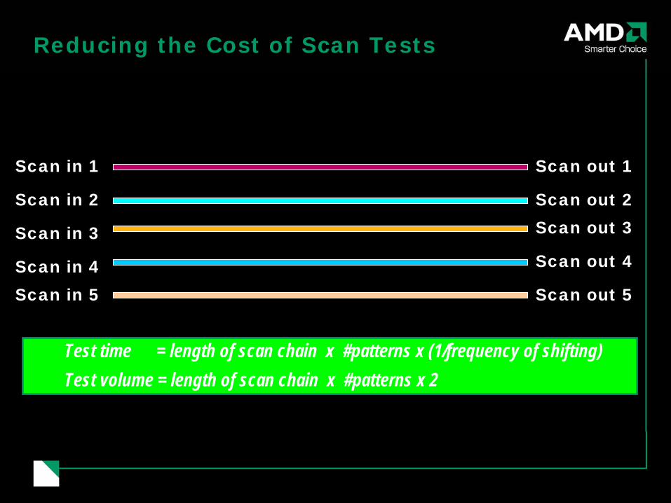
Reducing the Cost of Scan Tests
Scan in 1
Scan in 2
Scan in 3
Scan in 4Scan in 5
Scan out 1
Scan out 2Scan out 3
Scan out 4
Scan out 5
Test time = length of scan chain x #patterns x (1/frequency of shifting)Test volume = length of scan chain x #patterns x 2
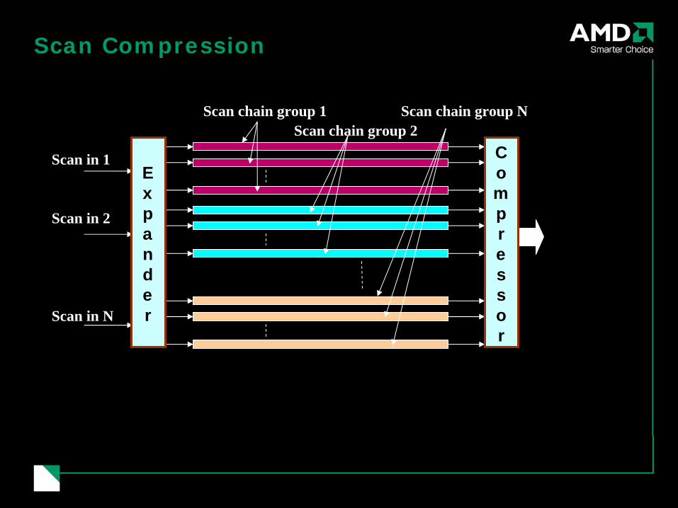
Scan Compression
Scan chain group 1Scan chain group 2
Scan chain group N
Scan in 1
Scan in 2
Scan in N
Expander
Compressor
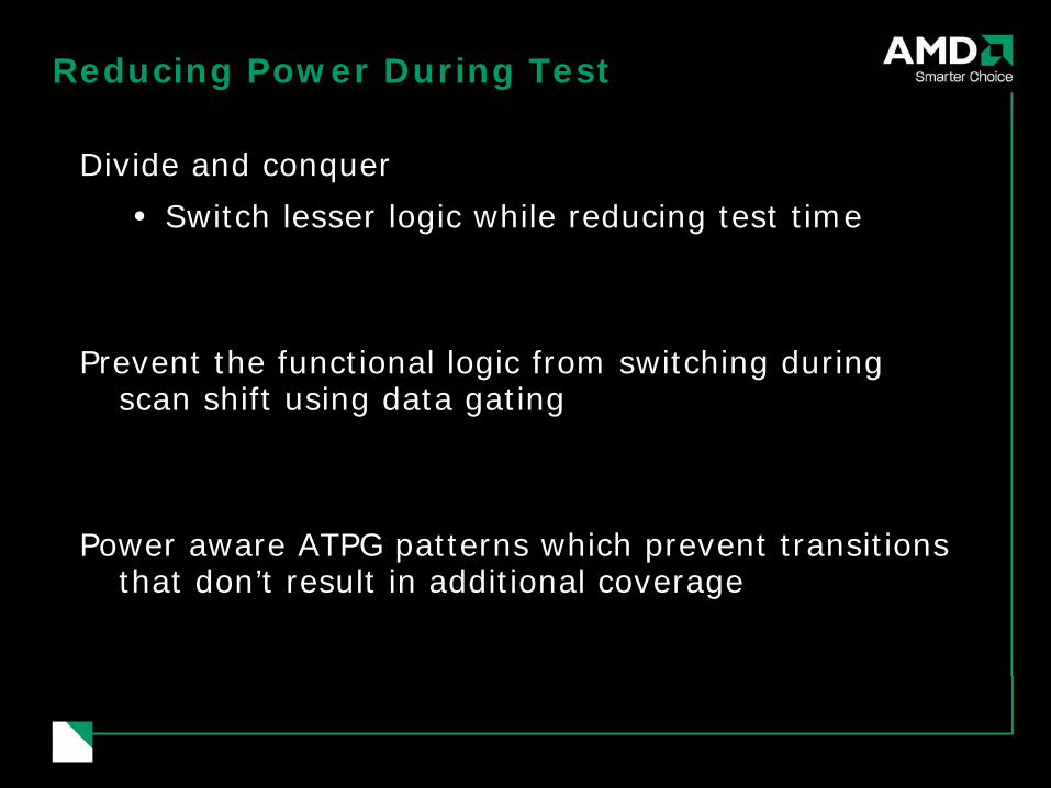
Reducing Power During Test
Divide and conquer
Switch lesser logic while reducing test time
Prevent the functional logic from switching during scan shift using data gating
Power aware ATPG patterns which prevent transitions that don’t result in additional coverage
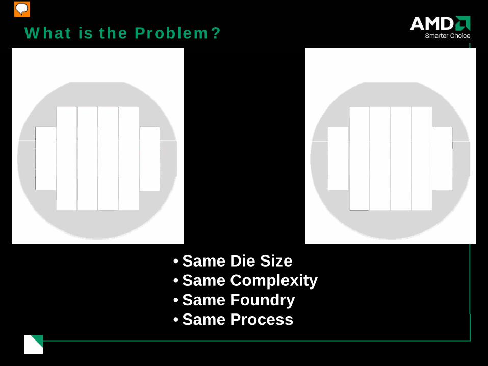
What is the Problem?
Design 2Design 1
• Same Die Size• Same Complexity• Same Foundry• Same Process
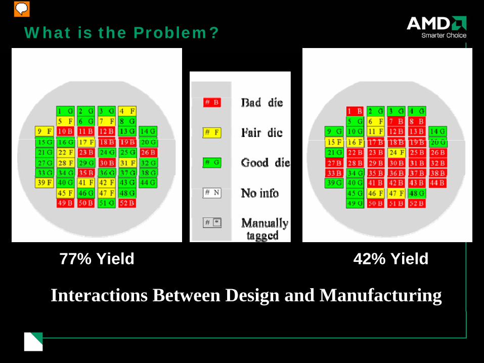
42% Yield77% Yield
What is the Problem?
Interactions Between Design and Manufacturing
Design 1 Design 2
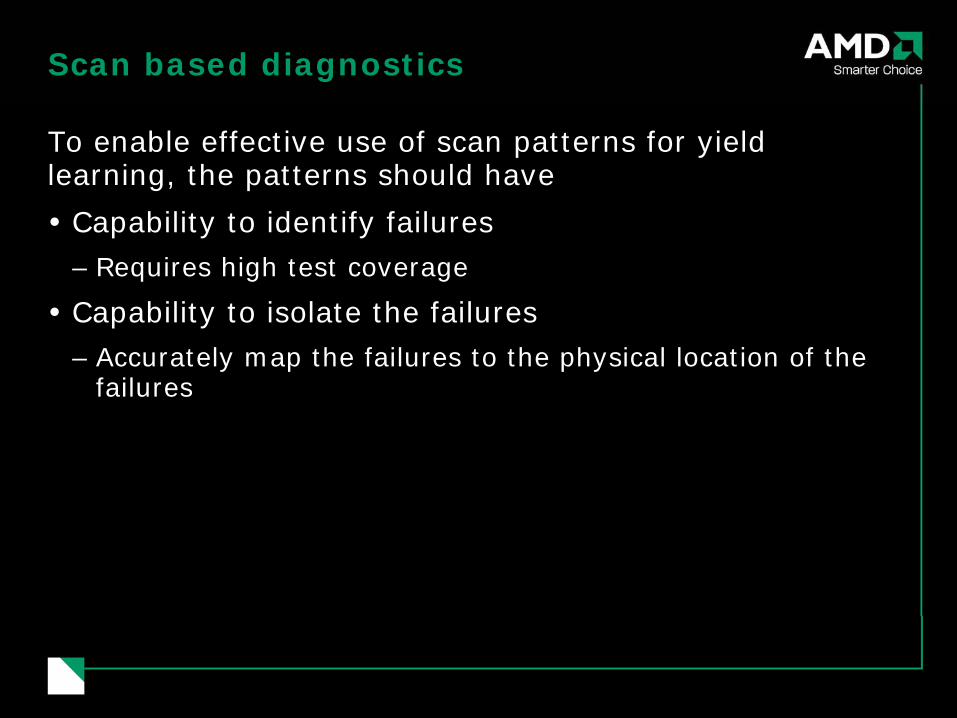
Scan based diagnostics
To enable effective use of scan patterns for yield learning, the patterns should have
Capability to identify failures– Requires high test coverage
Capability to isolate the failures– Accurately map the failures to the physical location of the
failures
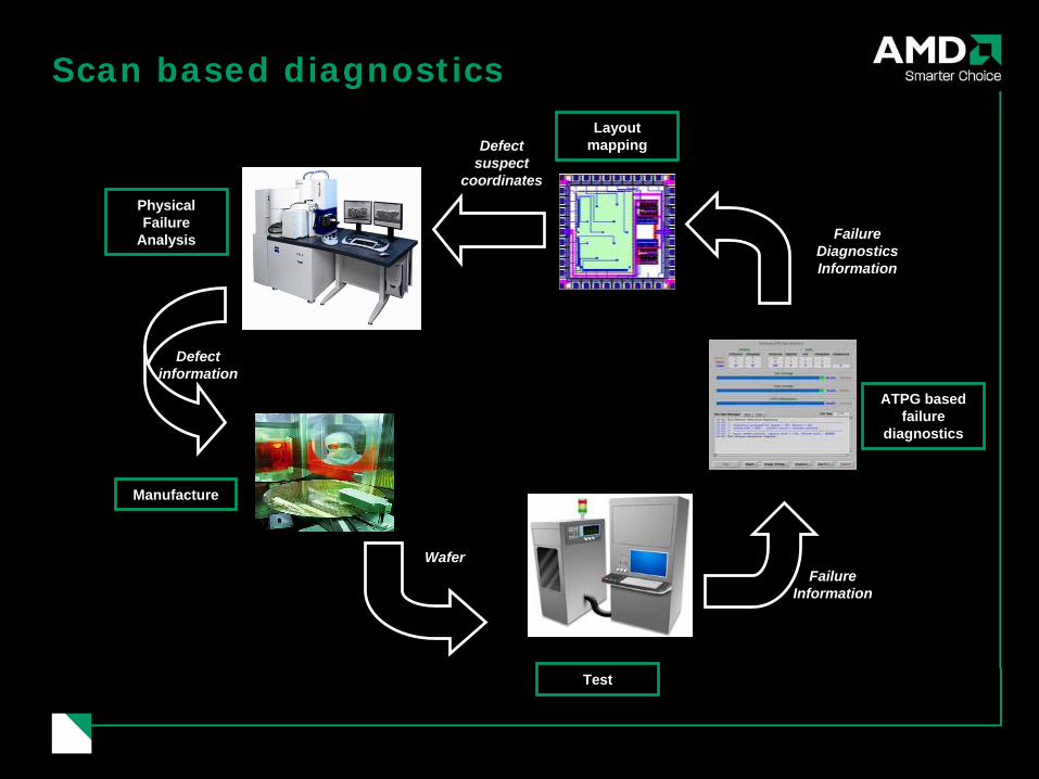
Scan based diagnostics
Failure Information
Failure Diagnostics Information
Defect suspect
coordinates
Defect information
Layout mapping
ATPG based failure
diagnostics
Physical Failure
Analysis
Manufacture
Test
Wafer
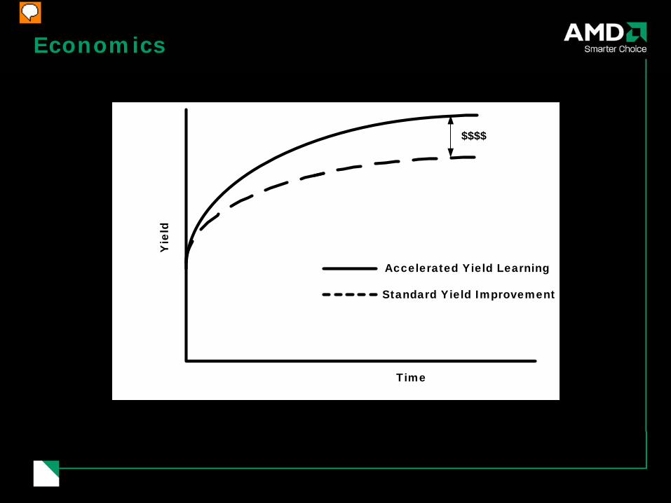
Economics
Yie
ld
Time
Standard Yield Improvement
Accelerated Yield Learning
$$$$
Conclusion
Nanometer testing presents new challenges not seen hitherto
Without a single-eyed focus on test, either of the following scenarios are likely:
Low Test Quality : High escape rates of defective devicesHigh Test Cost : Affecting profitabilitySlow ramp to volume : Missing critical time-to-market windows
The solution to these problems requires a tight interaction between the test experts, silicon technology experts and ATE experts


