Nanoscale Measurement Methods for Novel Material Characterization J. Alexander Liddle, Gila E. Stein, 1 Joseph A. Stroscio, Nikolai B. Zhitenev, P. N. First, 2 and W. A. de Heer 2 1 Department of Chemical & Biomolecular Engineering, University of Houston 2 School of Physics, Georgia Institute of Technology
Transcript
Nanoscale Measurement Methods for Novel Material Characterization
J. Alexander Liddle, Gila E. Stein,1 Joseph A. Stroscio, Nikolai B. Zhitenev,
P. N. First,2 and W. A. de Heer2
1Department of Chemical & Biomolecular Engineering, University of Houston2School of Physics, Georgia Institute of Technology
Diblock Copolymers for Advanced Patterning
Pitch and LER limit circuit density and device uniformity
Diblock copolymers might help Significant optimization needed How do we measure their behavior?
Diblock Copolymers
From “Block Copolymers - Designer Soft Materials”, F.S. Bates and G.H. Frederickson, Physics Today, Feb. 32 (1999)
Variations in duty cycle, coverage and line-edge roughness
200 nm
Diblock EpitaxyAFM SEM
No variation in duty cycle, coverage and line-edge roughness
5
Sub-Lithographic PatternsDense Self-Assembly on Sparse Chemical Patterns: Rectifying and Multiplying Lithographic Patterns Using Block Copolymers, Joy Y. Cheng, Charles T. Rettner, Daniel P. Sanders, Ho-Cheol Kim, and William D. Hinsberg, Advanced Materials, (2008) - IBM
Lithographic Pattern Diblock
Lithographic Pattern Diblock
P = 57.5 nm P = 28.8 nm
6
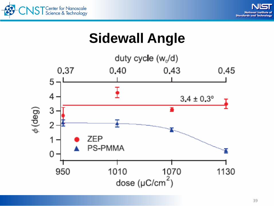
LER from SEM
7
ZEP
PS/PMMA
Resonant X-ray ScatteringAre interfaces sharp, chemically diffuse or rough?
X-ray scattering can measure interfacial widthor roughness to sub-0.5 nm accuracy.
Different chemistries have distinct resonances
Resonant scattering enhances contrast from different chemical domains
C=C π* 285 eV, C=O π* 288 eV, C-O σ* 293 eV
O O
Cl
O O
PS PMMA ZEP
8
Virgili et al. Macromolecules (2007)
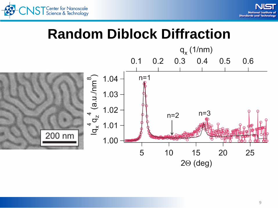
Random Diblock Diffraction
9
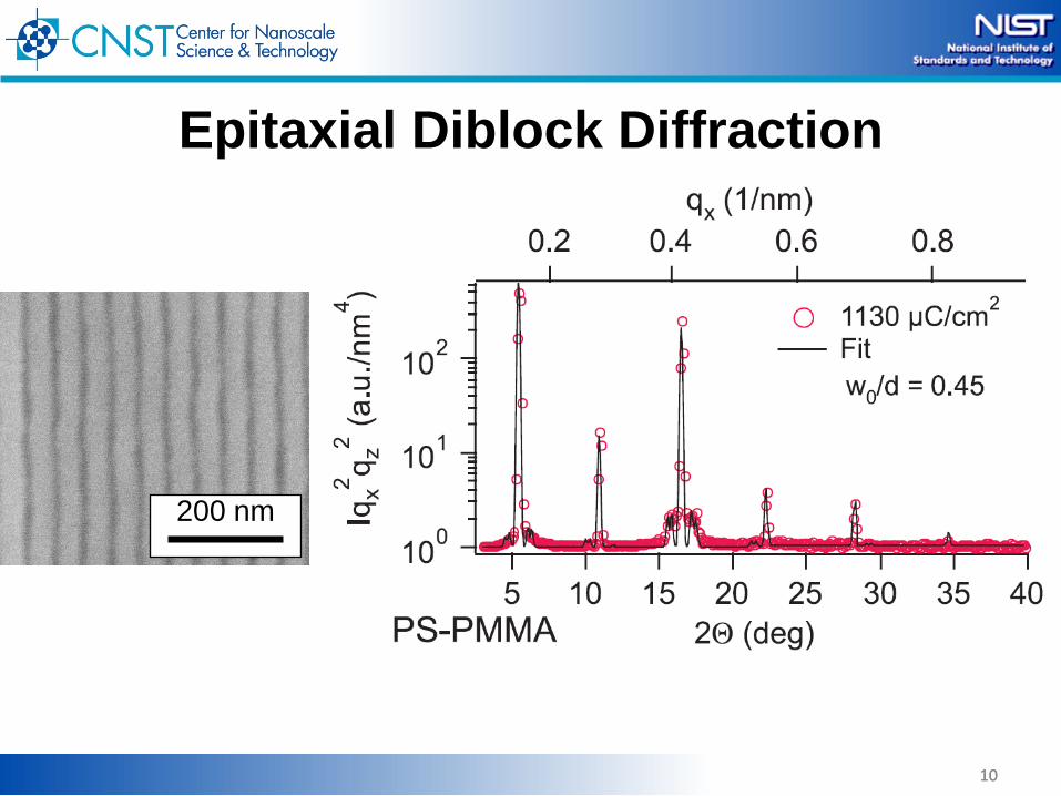
Epitaxial Diblock Diffraction
10
200 nm
10
Interface Width from XRD
11
200 nm
Summary X-ray diffraction samples large areas Resonant scattering provides chemical
contrast – diblocks, latent images, etc. Patterned nanostructure arrays yield
lots of information Analysis relies on model
12
Solar Cells for Large-area Electronics
Most work on material development, or device efficiency by trial and error
Correlation of film morphology and charge transport not known
Novel combined electrical and optical techniques needed
Organic PV Cell Donor and acceptor
separate charge carriers
Efficiency low in layered systems because of short exciton diffusion length
Nanostructured blends reduce required length
D A
Blended Organic Solar Cells
Bulk heterojunction
1:1 blend of Poly(3-hexylthiophene) (P3HT) to [6,6]-phenyl-C61-butyric acid methyl ester (PCBM).
SMUCathode
Anode
Glass substrate
Blended donor-acceptor molecules
SPM Photocurrent Measurements
Glass substrateAnode (TCO)
PV layer (~200 nm)
~acdc
532 nm laser focused into fiber optic cable
C-AFM tip
mirror
Photoresponse current measured with a conductive tip in contact mode while simultaneously mapping the surface topography.
Signal at each pixel can be used to construct a 2D conductance map of the surface.
Meas. unit
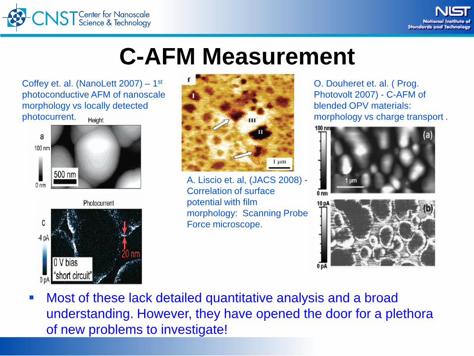
C-AFM Measurement
Most of these lack detailed quantitative analysis and a broad understanding. However, they have opened the door for a plethora of new problems to investigate!
Coffey et. al. (NanoLett 2007) – 1st
photoconductive AFM of nanoscalemorphology vs locally detected photocurrent.
A. Liscio et. al, (JACS 2008) -Correlation of surface potential with film morphology: Scanning Probe Force microscope.
O. Douheret et. al. ( Prog. Photovolt 2007) - C-AFM of blended OPV materials: morphology vs charge transport .
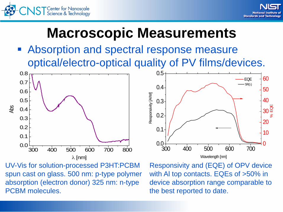
Macroscopic Measurements Absorption and spectral response measure
optical/electro-optical quality of PV films/devices.
300 400 500 600 700 8000.0
0.1
0.2
0.3
0.4
0.5
0.6
0.7
0.8
Abs
λ [nm]
300 400 500 600 7000.0
0.1
0.2
0.3
0.4
0.5
0
10
20
30
40
50
60
Res
pons
ivity
[A/W
]
Wavelength [nm]
SR(λ) EQE
% E
QE
UV-Vis for solution-processed P3HT:PCBM spun cast on glass. 500 nm: p-type polymer absorption (electron donor) 325 nm: n-type PCBM molecules.
Responsivity and (EQE) of OPV device with Al top contacts. EQEs of >50% in device absorption range comparable to the best reported to date.
Photocurrent vs Morphology 3-D topography overlaid with
local short-circuit photocurrent measurements of blended P3HT:PCBM film
Film prepared on top of TCO electrode modified by PEDOT:PSS.
Darker regions correspond to substantial photocurrent collection.
Photocurrent vs Bias Voltage
short circuit condition (V = 0 V)
forward bias(V = +0.3 V)
reversed bias(V = -0.3 V)
forward bias(V = +0.6 V)
reversed bias(V = -1 V)
forward bias(V = +1.5 V)
Summary
Photoconductive SPM is an important tool to study and characterize photovoltaic response of at the nm scale.
Demonstrated measurements with new results on a well-studied material system
Continue to add new imaging modalities
Graphene for Post-CMOS Electronics
CMOS approaching scaling limits Graphene more amenable to large-area
integration than CNTs Measurements of basic materials and
device properties needed
Graphene Production Methods
Mechanical exfoliation –scotch tape method K.S. Novoselov Proc. Natl. Acad. (2005) Single device process
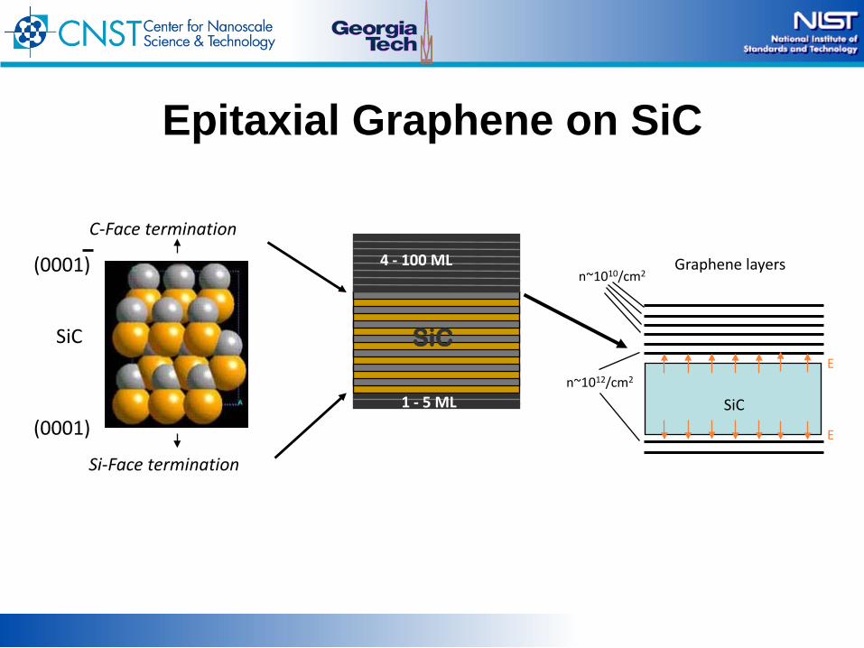
Epitaxial graphene on SiC C. Berger et al. J. Phys. Chem. (2004); Science (2006) Wafer scalable process
Courtesy of Suyoung Jung, NIST
Courtesy of Walt de Heer, GT
C-Face termination
Si-Face termination
SiC SiC
4 - 100 ML
1 - 5 ML
(0001)
(0001)
Graphene layers
n~1012/cm2
n~1010/cm2
E
E
SiC
Induction Furnace Method
Multilayers on C-face are electronically decoupledEpitaxial Graphene on C-face SiC
J. Hass et al., PRL 100, 1255504 (2008)Berger et al., J. Phys. Chem B 108, 19912 (2004)Berger et al., Science 312, 1191 (2006)de Heer et al., Sol. St. Commun., 143, 92 (2007)
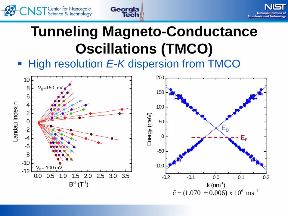
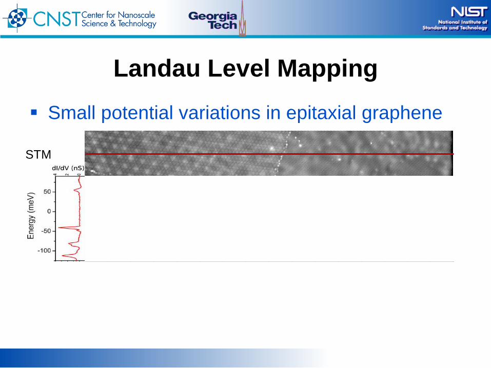
STM Measurement of Quantization Direct measurement of density of states with
scanning tunneling spectroscopy
Spatial LDOS mapping Probe the dI/dV(B,E) plane
Tip DOS Sample DOS
empty states
filled stateskBT
Topographic mode Spectroscopic mode T=4 K
/ LDOSdI dV ∝
Graphene Magnetic Quantization Hallmark of Graphene is the new Landau level
quantization and ½ integer QHE – LLs have unequal spacing, special n=0 level
Summary Epitaxial graphene on C-face SiC is a good candidate for
carbon based electronics
TMCO is a new STM measurement for high resolution low energy band structure
Direct measurement of the new graphene quantization with tunneling spectroscopy
Spatial mapping of LL offers great future potential to understand graphene physics
See Miller, Kubista, Rutter et al. Science (in press) and www.cnst.nist.gov
NIST
CNST Joseph Stroscio
Nikolai Zhitenev
Mark Stiles
Postdocs Gregory Rutter
Young Jae Song
Sander Otte
Suyong Jung
Honki Min
Visiting Fellow Young Kuk
EEEL Dave Newell
Curt Richter
Mark Keller
Physics Angie Hight
Walker MSEL
Jan Obrzut Eric Cockayne
Georgia Tech Professors
Phillip First
Walt de Heer
Students Lee Miller
Kevin Kubista
Ming Ruan
Univ. Texas Austin Professors
Allan MacDonald
GrapheneDiblocksNIST
CNST Alex Liddle
Postdoc Gila Stein
PhotovolataicsNIST
CNST Nikolai Zhitenev
Postdoc Behrang Hamadani
THANK YOU!
33
Backup Slides
Patterned Media for Hard DisksPatterned media require:Feature size < 20 nmSize control < 2 nm , 3σShort-range placement < 2 nm, 3σAreas > 10 cm2
Beyond the limits of top-down nanopatterning
Graphoepitaxy of Self-assembled Block Copolymers on Two Dimensional Periodic Patterned Templates, Ion Bita, Joel K.W. Yang, Yeon Sik Jung, Caroline A. Ross, Edwin L. Thomas, Karl K. Berggren, Science (2008)
35
Pattern NoiseEM noise
Barcode reader
Diffraction picks up subtle variations across large areas
Epitaxial graphene on SiC C. Berger et al. J. Phys. Chem. (2004); Science (2006)
Epitaxial Graphene on SiC
C-Face termination
Si-Face termination
SiC SiC
4 - 100 ML
1 - 5 ML
(0001)
(0001)
Graphene layers
n~1012/cm2
n~1010/cm2
E
E
SiC
Epitaxial Graphene on Si-face SiCC-Face termination
Si-Face termination
SiC SiC
4 - 100 ML
1 - 5 ML
(0001)
(0001)
Graphene layers
n~1012/cm2
n~1010/cm2
E
E
SiC
•Our previous work on UHV grown Si-face material•AB Bernal stacked epitaxial graphene•Intravalley and intervalley scattering; G. Rutter et al. Science (2007); JVST (2008) 10 nm
Previous STS Measurements on Graphite Surfaces
T. Matsui et al. PRL (2005) G. Li and E. Andrei Nature Phys. (2007)
Complex spectra Mixture of peaks
of linear and non-linear in B
Graphene Landau Quantization Multilayer epitaxial graphene on SiC is
“graphene”!
-300 -200 -100 0 100 200 3000
5
10
15
20
25
30
6 T
5 T
4 T
3 T
2 T
1 T
dI/d
V (n
S)
Sample Bias (mV)
0 T
sgn( ) 2 , ... 2, 1,0,1, 2,...nE n c e B n n= = − −
0 1 2 3 4 5 6 7 8-5
0
5
10
15
20
-8 -7 -6 -5 -4 -3 -2 -1 0 1 2 3 4 5 6 7 8
-300
-200
-100
0
100
200
300
LLn=
0 (m
eV)
B (T)
LLn -
LL n=
0 (m
eV)
Sgn(n)(|n|B)1/2
1 T 2 T 3 T 4 T 5 T 6 T 7 T 8 T
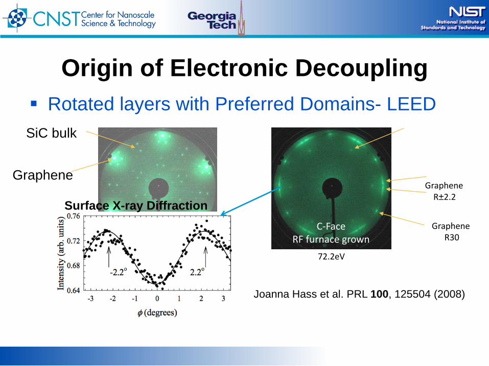
Origin of Electronic Decoupling
Layer stacking
R30
R31.5R-3.6
R7R31.5C
R30C
Alternating between:NEAR 30˚ & NEAR 0˚
Joanna Hass et al. PRL 100, 125504 (2008)
Origin of Electronic Decoupling
Rotated layers – STM Moiré patterns
Rotational Domain Boundaries
Atomically flat and continuous across boundary
400 nm
50 pm
Rotational Domain Boundaries
20 nm 8 nm
Graphene Landau Quantization Complete field scaling of graphene quantization
-300 -200 -100 0 100 200 3000
5
10
15
20
25
30
6 T
5 T
4 T
3 T
2 T
1 T
dI/d
V (n
S)
Sample Bias (mV)
0 T
sgn( ) 2 , ... 2, 1,0,1, 2,...nE n c e B n n= = − −
0 1 2 3 4 5 6 7 8-5
0
5
10
15
20
-8 -7 -6 -5 -4 -3 -2 -1 0 1 2 3 4 5 6 7 8
-300
-200
-100
0
100
200
300
LLn=
0 (m
eV)
B (T)
LLn -
LL n=
0 (m
eV)
Sgn(n)(|n|B)1/2
1 T 2 T 3 T 4 T 5 T 6 T 7 T 8 T
Magnetic Quantization
Cyclotron motion in a magnetic field Quantized orbits and energy levels
Magneto-oscillations De Haas-van Alphen and Shubnikov-de Hass effects;
oscillations in physical properties due to quantization of density of states
Tunneling magneto-conductance oscillations
B* ( 1/ 2) 0n
eBE n nm
= + ≥
2sgn( ) 2 n=0, 1...nE n e c n B= ±
Standard 2DEG
Graphene
Tunneling Magneto-Conductance Oscillations (TMCO)
Fixing E and sweeping B
01234567
0.0 0.5 1.0 1.5 2.0012345
01234567
VB=-55 mV
-7
dI/d
V (n
S)
n=-3
-4-5
-6
B (T)
-9-8
VB=-65 mV
-7
n=-4-5
dI/d
V (n
S) -6
-6 -5-4
dI/d
V (n
S)
n=-3VB=-45 mV
F F( / 2 )B e Aπ= F EA A→
Analogous to Shubnikov-de Haas oscillations but with one big difference
Allows low energy band structure to be measured with high energy and momentum resolution
Origin of Electronic Decoupling Rotated layers with Preferred Domains- LEED