21
McGraw-Hill Copyright © 2001 by the McGraw-Hill Companies, Inc. All rights reserved. 16-1 Chapter Sixteen MOSFET Digital Circuits

McGraw-Hill Copyright © 2001 by the McGraw-Hill Companies, Inc. All rights reserved.
16-1Chapter Sixteen
MOSFET Digital Circuits

McGraw-Hill Copyright © 2001 by the McGraw-Hill Companies, Inc. All rights reserved.
16-2Figure 16.6Voltage transfer characteristics, NMOS inverter with resistor load, for three resistor values

McGraw-Hill Copyright © 2001 by the McGraw-Hill Companies, Inc. All rights reserved.
16-3Figure 16.8(a) NMOS inverter with saturated load and (b) driver transistor characteristics and load curve
McGraw-Hill Copyright © 2001 by the McGraw-Hill Companies, Inc. All rights reserved.
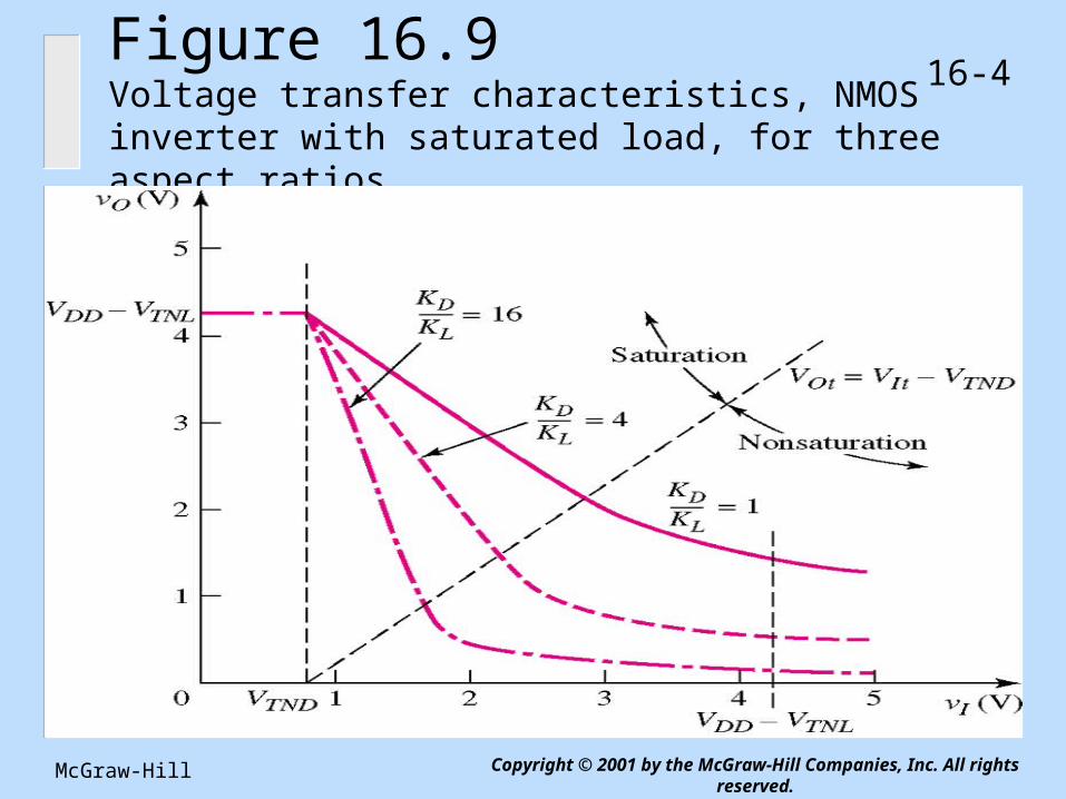
16-4Figure 16.9Voltage transfer characteristics, NMOS inverter with saturated load, for three aspect ratios
McGraw-Hill Copyright © 2001 by the McGraw-Hill Companies, Inc. All rights reserved.
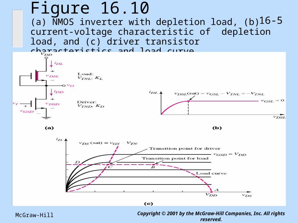
16-5Figure 16.10(a) NMOS inverter with depletion load, (b) current-voltage characteristic of depletion load, and (c) driver transistor characteristics and load curve

McGraw-Hill Copyright © 2001 by the McGraw-Hill Companies, Inc. All rights reserved.
16-6Figure 16.11Voltage transfer characteristics, NMOS inverter with depletion load, for three aspect ratios

McGraw-Hill Copyright © 2001 by the McGraw-Hill Companies, Inc. All rights reserved.
16-7Figure 16.18Voltage transfer characteristics of NMOS inverters with and without the body effect (a) enhancement load and (b) depletion load
McGraw-Hill Copyright © 2001 by the McGraw-Hill Companies, Inc. All rights reserved.
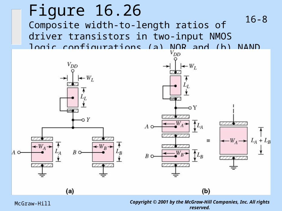
16-8Figure 16.26Composite width-to-length ratios of driver transistors in two-input NMOS logic configurations (a) NOR and (b) NAND

McGraw-Hill Copyright © 2001 by the McGraw-Hill Companies, Inc. All rights reserved.
16-9Figure 16.27NMOS logic circuit example

McGraw-Hill Copyright © 2001 by the McGraw-Hill Companies, Inc. All rights reserved.
16-10Figure 16.34CMOS inverter

McGraw-Hill Copyright © 2001 by the McGraw-Hill Companies, Inc. All rights reserved.
16-11Figure 16.39Complete voltage transfer characteristics, CMOS inverter

McGraw-Hill Copyright © 2001 by the McGraw-Hill Companies, Inc. All rights reserved.
16-12Figure 16.41Square root of inverter current versus input voltage, CMOS inverter biased at either VDD = 5V or VDD = 10V

McGraw-Hill Copyright © 2001 by the McGraw-Hill Companies, Inc. All rights reserved.
16-13Figure 16.44(a) Two-input CMOS NOR logic circuit and (b) truth table

McGraw-Hill Copyright © 2001 by the McGraw-Hill Companies, Inc. All rights reserved.
16-14Figure 16.45(a) Two-input CMOS NAND logic circuit and (b) truth table
McGraw-Hill Copyright © 2001 by the McGraw-Hill Companies, Inc. All rights reserved.
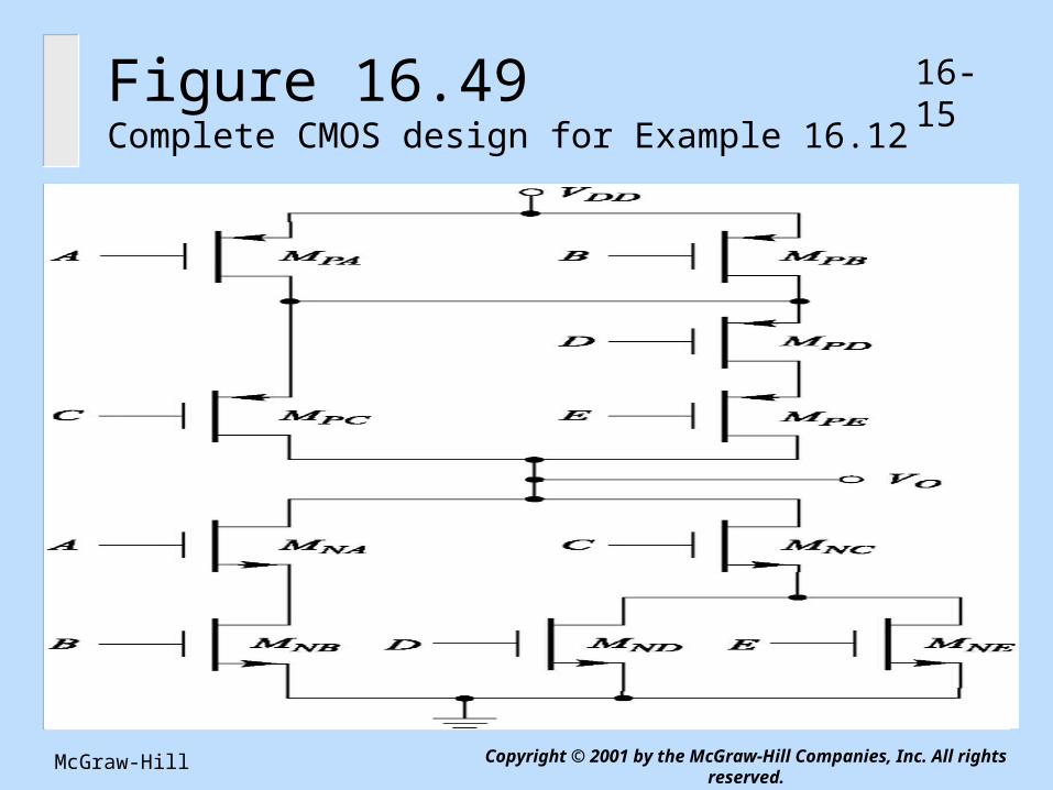
16-15Figure 16.49Complete CMOS design for Example 16.12

McGraw-Hill Copyright © 2001 by the McGraw-Hill Companies, Inc. All rights reserved.
16-16Figure 16.52Clocked CMOS logic circuit (a) AND function and (b) OR function
McGraw-Hill Copyright © 2001 by the McGraw-Hill Companies, Inc. All rights reserved.
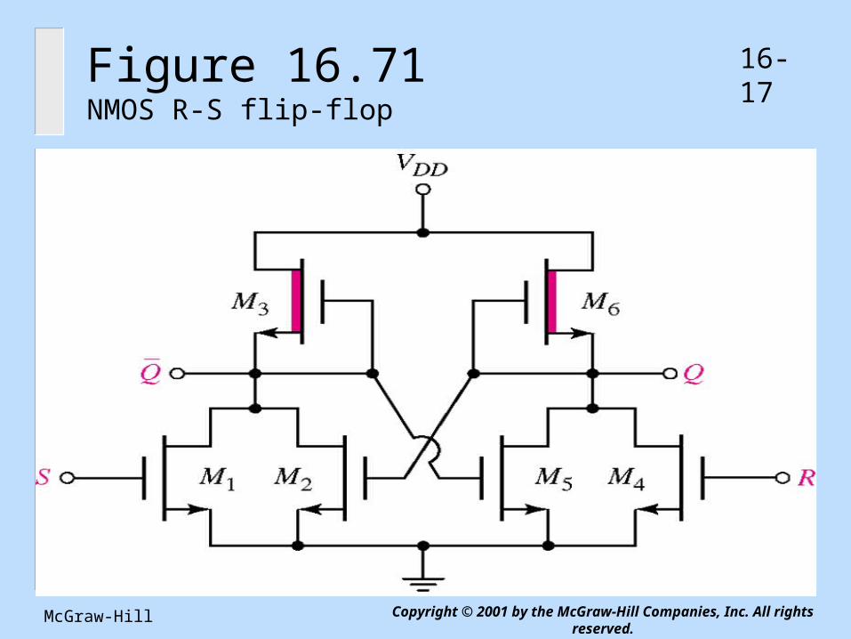
16-17Figure 16.71NMOS R-S flip-flop

McGraw-Hill Copyright © 2001 by the McGraw-Hill Companies, Inc. All rights reserved.
16-18Figure 16.72CMOS R-S flip-flop
McGraw-Hill Copyright © 2001 by the McGraw-Hill Companies, Inc. All rights reserved.
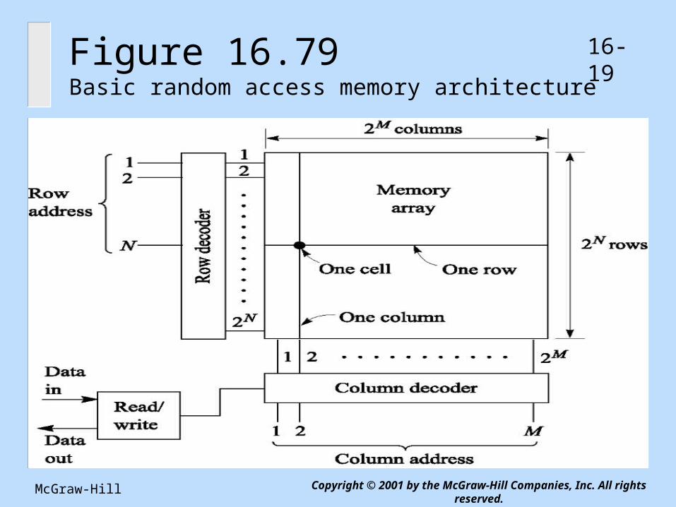
16-19Figure 16.79Basic random access memory architecture

McGraw-Hill Copyright © 2001 by the McGraw-Hill Companies, Inc. All rights reserved.
16-20Figure 16.84CMOS RAM cell including PMOS pull-up transistors

McGraw-Hill Copyright © 2001 by the McGraw-Hill Companies, Inc. All rights reserved.
16-21Figure 16.87 Complete circuit diagram of a CMOS RAM cell with write and read circuitry


