EE 230 inverters – 1 resistively-loaded NMOS inverter Since the drain current depends on the gate voltage (= v i ), it is easy to relate the output to the input. Determining the complete voltage transfer characteristic involves finding v o as a function of v i for all possible operating modes of the NMOS (off, saturation, ohmic) and putting the pieces together into a single characteristic. We have seen the circuit at right while practicing our NMOS skills. Now we note that it is an implementation of a simple inverter. The inverter input voltage is v GS and the output is v DS . v o = v DS = V DD – i D R D . In principle, the output voltage can range from 0 to V DD . This also defines the range of the input voltage. V DD i D v o = v DS R D v i = v GS – + v DS – + v GS
Transcript
EE 230 inverters – �1
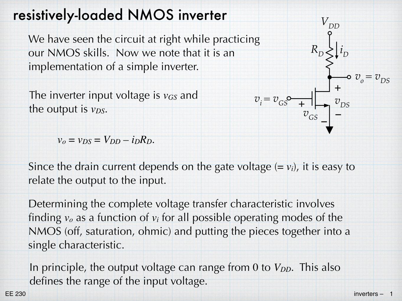
resistively-loaded NMOS inverter
Since the drain current depends on the gate voltage (= vi), it is easy to relate the output to the input.
Determining the complete voltage transfer characteristic involves finding vo as a function of vi for all possible operating modes of the NMOS (off, saturation, ohmic) and putting the pieces together into a single characteristic.
We have seen the circuit at right while practicing our NMOS skills. Now we note that it is an implementation of a simple inverter.
The inverter input voltage is vGS and the output is vDS.
vo = vDS = VDD – iDRD.
In principle, the output voltage can range from 0 to VDD. This also defines the range of the input voltage.
VDD
iD
vo = vDS
RD
vi = vGS
–
+vDS
–+vGS
EE 230 inverters – �2
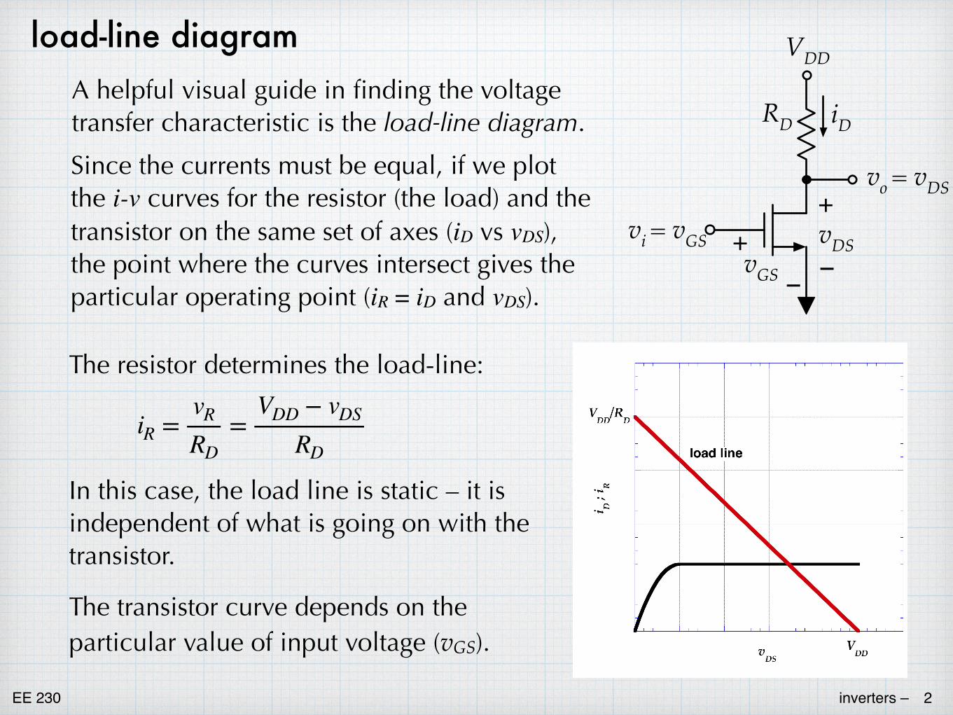
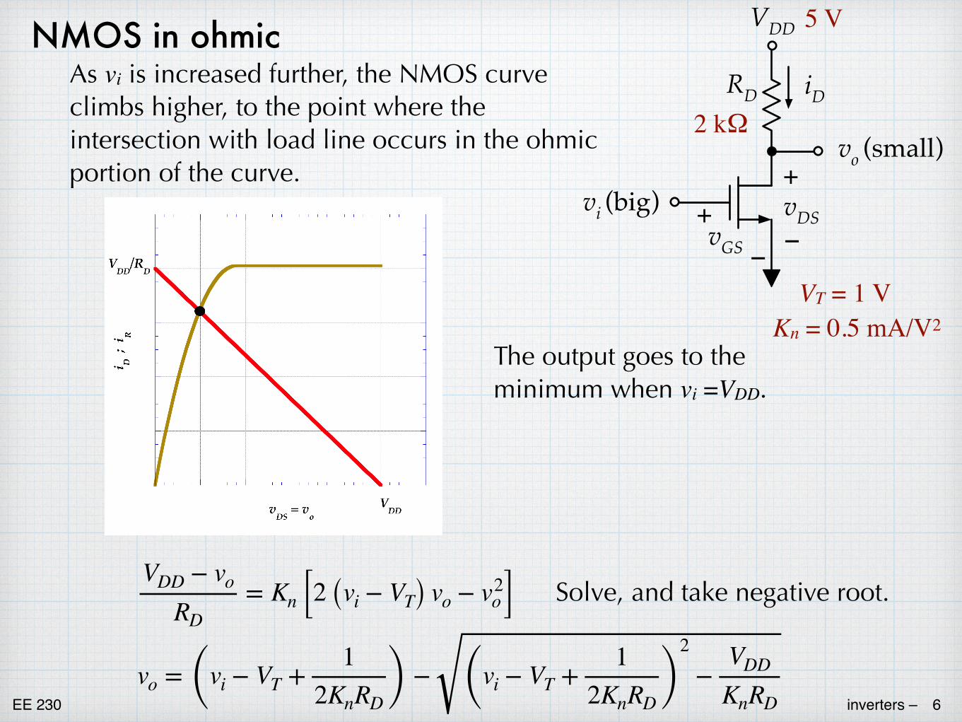
load-line diagramA helpful visual guide in finding the voltage transfer characteristic is the load-line diagram.
The resistor determines the load-line:
Since the currents must be equal, if we plot the i-v curves for the resistor (the load) and the transistor on the same set of axes (iD vs vDS), the point where the curves intersect gives the particular operating point (iR = iD and vDS).
In this case, the load line is static – it is independent of what is going on with the transistor.
The transistor curve depends on the particular value of input voltage (vGS).
VDD
iD
vo = vDS
RD
vi = vGS
–
+vDS
–+vGS
iR =vR
RD=
VDD − vDS
RD
EE 230 inverters – �3
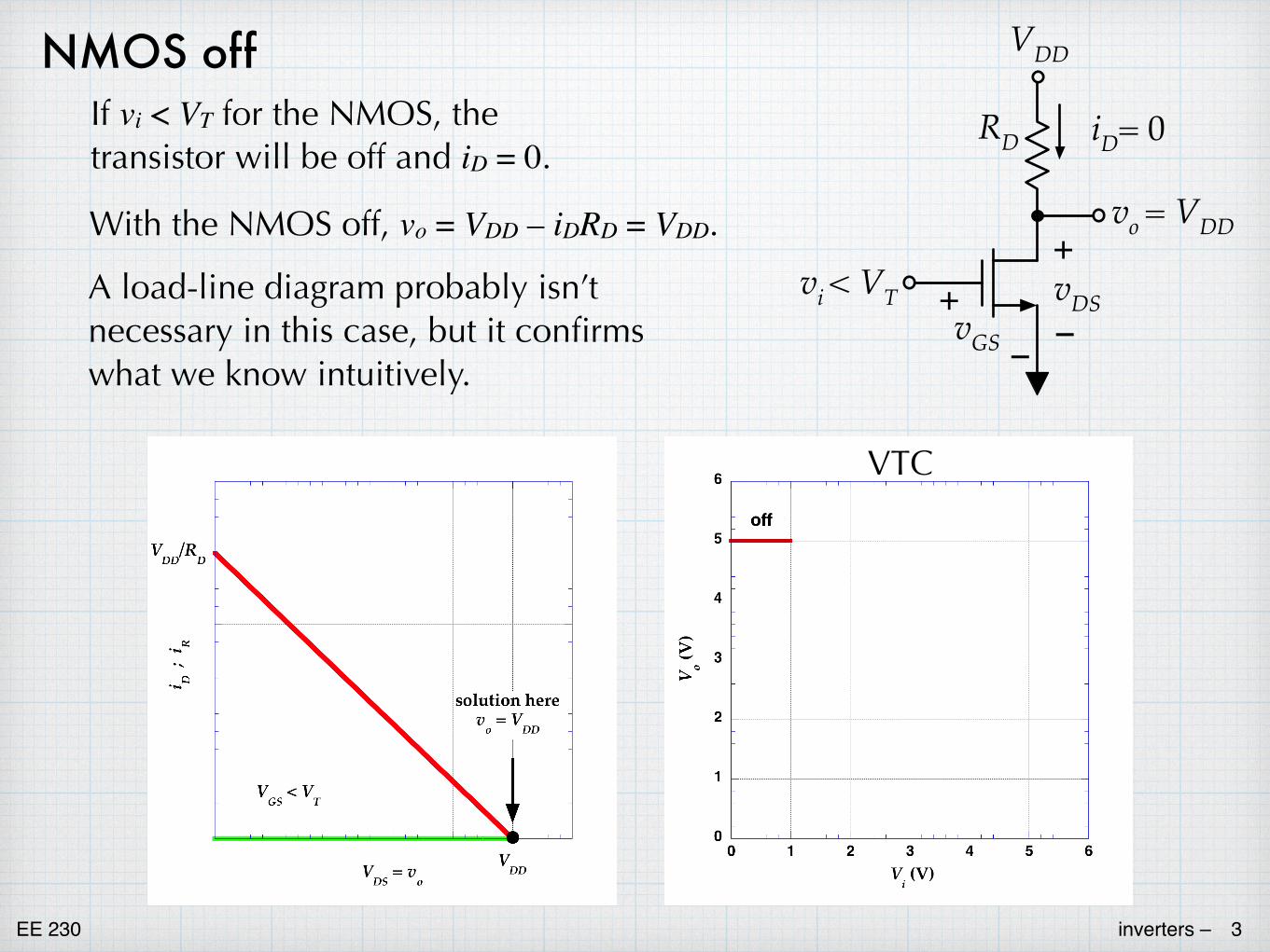
NMOS offIf vi < VT for the NMOS, the transistor will be off and iD = 0.
With the NMOS off, vo = VDD – iDRD = VDD.
A load-line diagram probably isn’t necessary in this case, but it confirms what we know intuitively.
VDD
iD= 0
vo = VDD
RD
vi < VT
–
+vDS
–+vGS
VTC
EE 230 inverters – �4
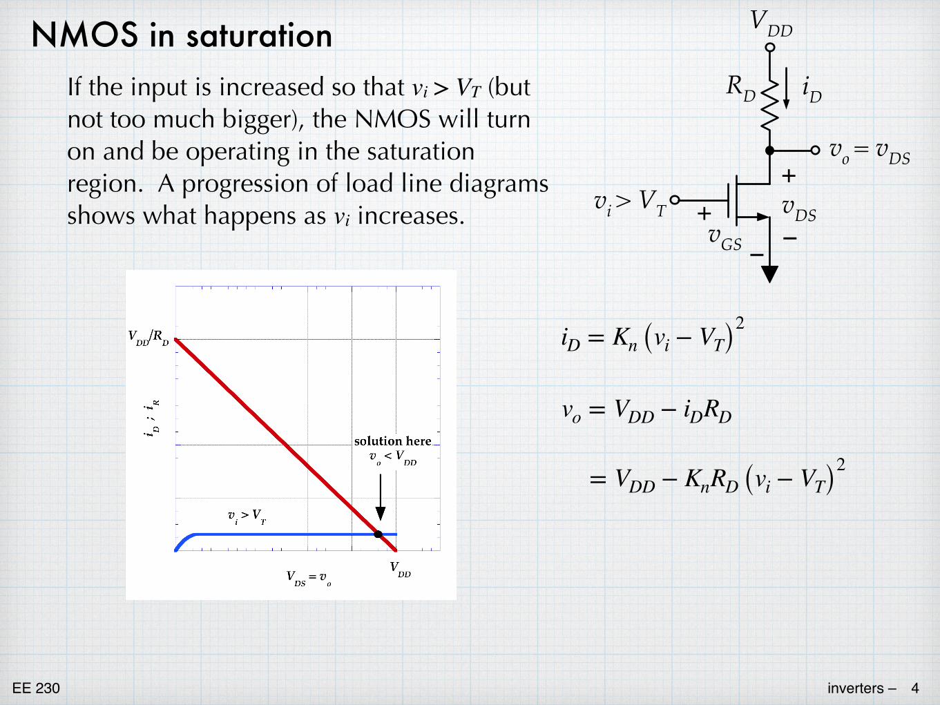
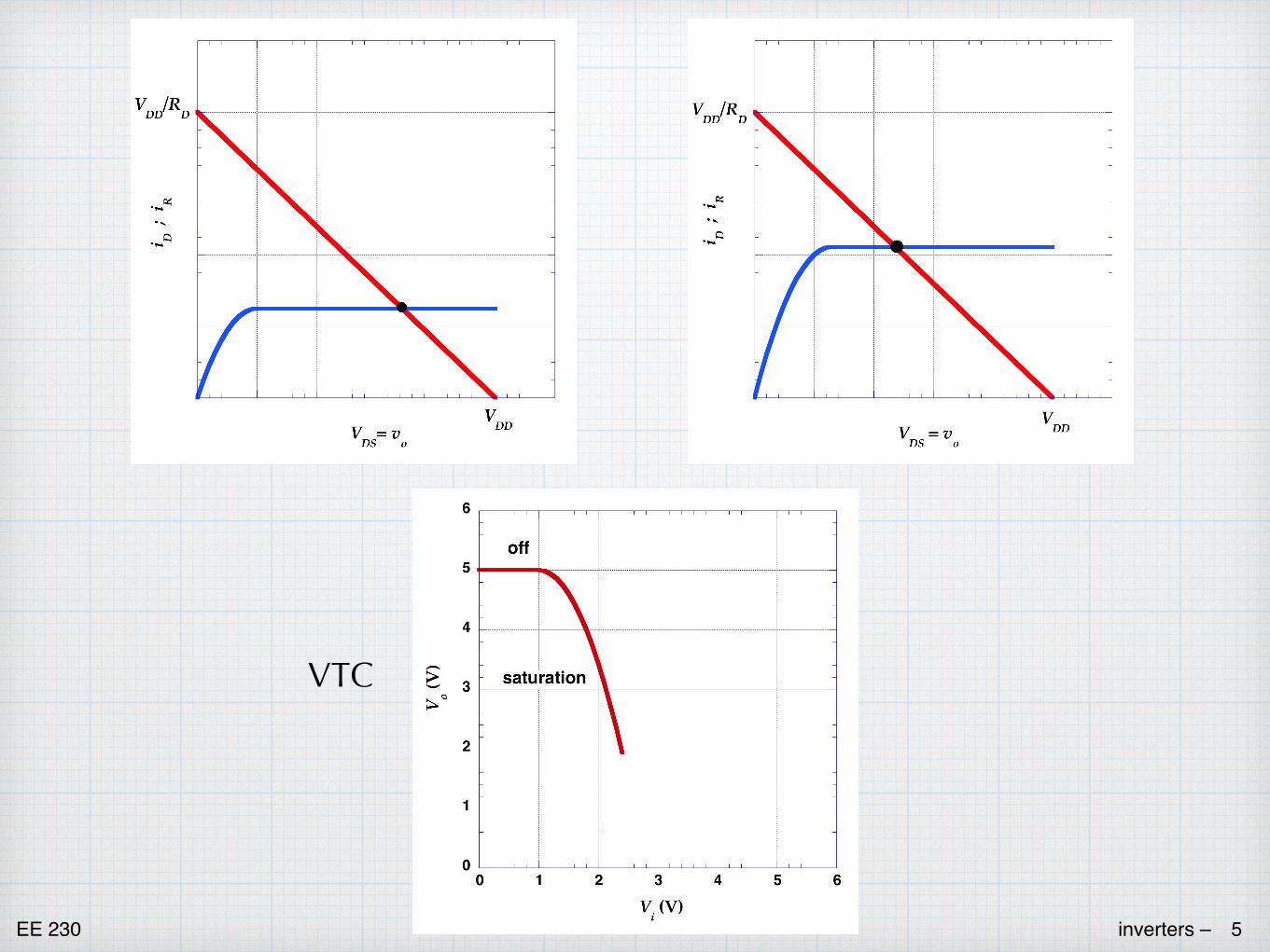
NMOS in saturationIf the input is increased so that vi > VT (but not too much bigger), the NMOS will turn on and be operating in the saturation region. A progression of load line diagrams shows what happens as vi increases.
VDD
iD
vo = vDS
RD
vi > VT
–
+vDS
–+vGS
iD = Kn (vi − VT)2
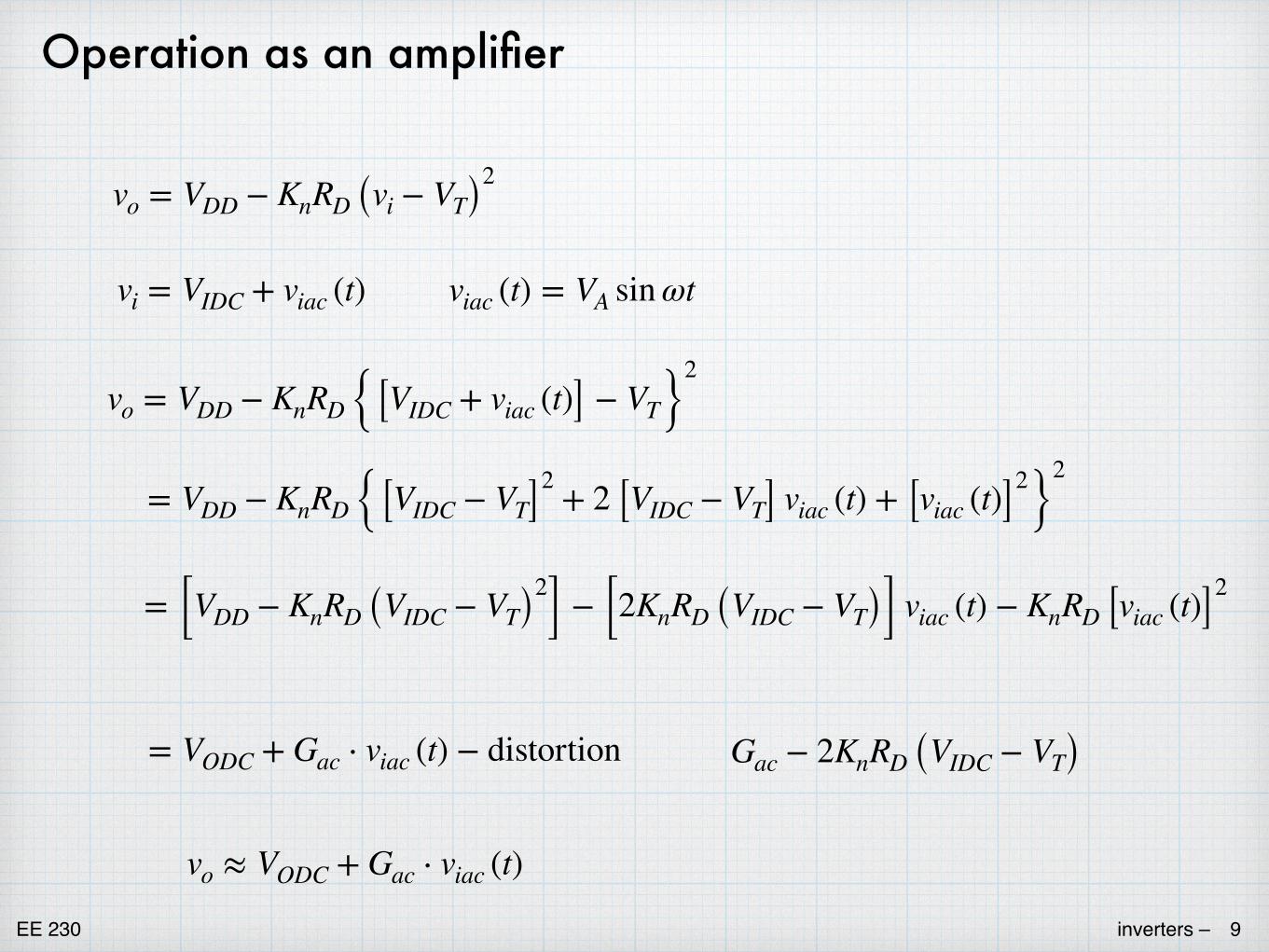
vo = VDD − iDRD
= VDD − KnRD (vi − VT)2
EE 230 inverters – �5
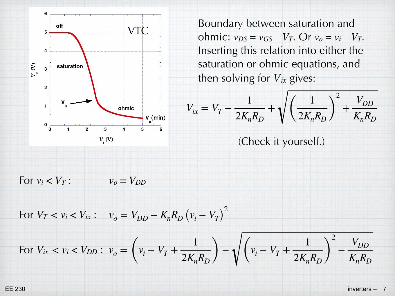
VTC
EE 230 inverters – �6
NMOS in ohmicAs vi is increased further, the NMOS curve climbs higher, to the point where the intersection with load line occurs in the ohmic portion of the curve.
VDD
iD
vo (small)
RD
vi (big)–
+vDS
–+vGS
The output goes to the minimum when vi =VDD.
VDD − vo
RD= Kn [2 (vi − VT) vo − v2
o]vo = (vi − VT +
12KnRD ) − (vi − VT +
12KnRD )
2
−VDD
KnRD
Solve, and take negative root.
2 kΩ
5 V
VT = 1 VKn = 0.5 mA/V2
EE 230 inverters – �7
For vi < VT : vo = VDD
For VT < vi < Vix :
For Vix < vi < VDD :
Boundary between saturation and ohmic: vDS = vGS – VT. Or vo = vi – VT. Inserting this relation into either the saturation or ohmic equations, and then solving for Vix gives:
VTC
(Check it yourself.)
vo = (vi − VT +1
2KnRD ) − (vi − VT +1
2KnRD )2
−VDD
KnRD
Vix = VT −1
2KnRD+ ( 1
2KnRD )2
+VDD
KnRD
vo = VDD − KnRD (vi − VT)2
EE 230 inverters – �8
Digital operationTo get some sense of how the inverter functions as a logic device, cascade one after the other.
If the input to the first inverter is VDD, it’s output will be vo(min) = . Then the input to the second inverter is , and so it’s output will be VDD.
As long as the input is “low enough” the inverter will give an output of VDD. As long the input is “high enough” the inverter will give an output that is “low” (low enough that the next gate will correctly interpret it as logic 0.
This is the power of digital circuitry — voltages don’t have to be precise. In this case, “close” is good enough.