66
Liquid Crystal Display Television Service Manual Chassis: MST6E16JS Product Type:LCD24V88APAM Ver 1.0 Hisense Electric Co.,Ltd. May, 2012
| Date post: | 13-Apr-2016 |
| Category: |
Documents |
| Upload: | antoniocesarutrera |
| View: | 148 times |
| Download: | 18 times |

Liquid Crystal Display Television
Service Manual
Chassis: MST6E16JS
Product Type:LCD24V88APAM
Ver 1.0
Hisense Electric Co.,Ltd.
May, 2012

- 2 -
Contents Contents ................................................................................................................................................................- 2 -
Service Manual ....................................................................................................................................................- 2 -
1. Precautions and notices..............................................................................................................................- 3 -
1.1 WARNING ......................................................................................................................................- 4 -
1.2 NOTES ............................................................................................................................................- 7 -
2. Factory/Service OSD Menu and Adjustment...........................................................................................- 10 -
2.1 To enter the Factory OSD Menu....................................................................................................- 10 -
2.2 Factory OSD Menu........................................................................................................................- 10 -
3. Software Upgrading.................................................................................................................................- 15 -
Before upgrading, read the following. .................................................................................................- 15 -
3.1 Get ready for upgrading.................................................................................................................- 15 -
3.2 Upgrading with the ISP_TOOL4.0.9 .............................................................................................- 25 -
3.3 USB Software upgrading ...............................................................................................................- 29 -
4. Circuit instruction ....................................................................................................................................- 34 -
4.1 Main board Power assign and block diagram................................................................................- 34 -
4.2 Image and signal process ...............................................................................................................- 35 -
4.3 The main IC description ................................................................................................................- 41 -
4.4 Troubleshooting .............................................................................................................................- 49 -
4.4.1 Troubleshooting for Remote Control ..................................................................................- 49 -
4.4.2 Troubleshooting for Function Key......................................................................................- 50 -
4.4.3 TV won’t Power On............................................................................................................- 51 -
4.4.4 Troubleshooting for Audio..................................................................................................- 52 -
4.4.5 Troubleshooting for TV/VGA/HDMI input........................................................................- 53 -
4.4.6 Troubleshooting for YPbPr input........................................................................................- 54 -
4.4.7 Troubleshooting for Video/S-Video input...........................................................................- 55 -
5. Schematic circuit diagram .......................................................................................................................- 56 -
Service Manual

- 3 -
1. Precautions and notices
BEFORE SERVICING THE LCD TV, READ THE SAFETY PRECAUTIONS IN
THIS MANUAL.
WHEN REPLACEMENT PARTS ARE REQUIRED, BE SURE TO USE
REPLACEMENT PARTS SPECIFIED BY THE MANUFACTURER.
Proper service and repair is important to the safe, reliable operation of all Hisense
Electric Co., Ltd Equipment. The service procedures recommended by Hisense and
described in this Service Guide are effective methods of performing service
operations. Some of these service operations require the use of tools specially
designed for the purpose. The special tools should be used when and as
recommended.
It is important to note that this manual contains various CAUTIONS and NOTICES
which should be carefully read in order to minimize the risk of personal injury to
service personnel. The possibility exists that improper service methods may damage
the equipment. It is also important to understand that these CAUTIONS and
NOTICES ARE NOT EXHAUSTIVE. Hisense could not possibly know, evaluate
and advise the service trade of all conceivable ways in which service might be done
or of the possible hazardous consequences of each way. Consequently, Hisense has
not undertaken any such broad evaluation. Accordingly, a serviceman that uses a
service procedure or tools, which are not recommended by Hisense, must first satisfy

- 4 -
himself thoroughly that neither his safety nor the safe of the equipment will be
jeopardized by the service method selected.
Hereafter throughout this manual, Hisense Electric Co., Ltd will be referred to as
Hisense.
1.1 WARNING
1.1.1
Critical components having special safety characteristics are identified with a by
the Ref. No. in the parts list. Use of substitute replacement parts, which do not have
the same specified safety characteristics, may create shock, fire, or other hazards.
Under no circumstances should the original design be modified or altered without
written permission from Hisense. Hisense assumes no liability, express or implied,
arising out of any unauthorized modification of design. Serviceman assumes all
liability.
1.1.2.
All ICs and many other semiconductors are susceptible to electrostatic discharges
DANGER CAUTION
TO ENSURE THE CONTINUED RELIABILITY OF THIS PRODUCT, USE ONLY
ORIGINAL MANUFACTURER'S REPLACEMENT PARTS, WHICH ARE LISTED WITH
THEIR PART NUMBERS IN THE PARTS LIST SECTION OF THIS SERVICE GUIDE.
- 5 -
(ESD). Careless handling during repair can reduce life drastically. When repairing,
make sure that you are connected with the same potential as the mass of the set by a
wristband with resistance. Keep components and tools also at this same potential.
1. Never replace modules or other components while the unit is switched on.
2. When making settings, use plastic rather than metal tools. This will prevent
any short circuits and the danger of a circuit becoming unstable.
1.1.3
To prevent electrical shock, do not use this polarized ac plug with an extension cord,
receptacle, or the outlet unless the blades can be fully inserted to prevent blade
exposure.
To prevent electrical shock, match wide blade or plug to wide slot, fully insert.
1.1.4
When replacement parts are required, be sure to use replacement parts specified by
the manufacturer or have the same characteristics as the original part. Unauthorized
substitutions may result in fire, electric shock, or other hazards.
1.1.5
Safety regulations require that after a repair the set must be returned in its original
condition. In particular attention should be paid to the following points.
-Note: The wire trees should be routed correctly and fixed with the mounted
cable clamps.
-The insulation of the mains lead should be checked for external damage.

- 6 -
1.1.6
(1) Do not touch Signal and Power Connector while this product operates. Do not
touch EMI ground part and Heat Sink of Film Filter.
(2) Do not supply a voltage higher than that specified to this product. This may
damage the product and may cause a fire.
(3) Do not use this product in locations where the humidity is extremely high,
where it may be splashed with water, or where flammable materials surround it. Do
not install or use the product in a location that does no satisfy the specified
environmental conditions. This may damage the product and may cause a fire.
(4) If a foreign substance (such as water, metal, or liquid) gets inside the panel
module, immediately turn off the power. Continuing to use the product may cause
fire or electric shock.
(5) If the product emits smoke, and abnormal smell, or makes an abnormal sound,
immediately turn off the power. Continuing to use the product, it may cause fire or
electric shock.
(6) Do not disconnect or connect the connector while power to the product is on. It
takes some time for the voltage to drop to a sufficiently low level after the power
has been turned off. Confirm that the voltage has dropped to a safe level before
disconnecting or connecting the connector.
(7) Do not pull out or insert the power cable from/to an outlet with wet hands. It
may cause electric shock.

- 7 -
(8) Do not damage or modify the power cable. It may cause fire or electric shock.
(9) If the power cable is damaged, or if the connector is loose, do not use the
product: otherwise, this can lead to fire or electric shock.
(10) If the power connector or the connector of the power cable becomes dirty or
dusty, wipe it with a dry cloth. Otherwise, this can lead to fire.
(11) Use only with the cart, stand, tripod, bracket, or table specified by the
manufacturer, or sold with the apparatus. When a cart is used, use caution when
moving the cart/apparatus combination to avoid injury from tip-over.
1.2 NOTES
Notes on Safe Handling of the LCD panel and during service
The work procedures shown with the Note indication are important for ensuring the
safety of the product and the servicing work. Be sure to follow these instructions.
• Before starting the work, secure a sufficient working space.
• At all times other than when adjusting and checking the product, be sure to turn
OFF the POWER Button and disconnect the power cable from the power source of
the TV during servicing.
• To prevent electric shock and breakage of PC board, start the servicing work at least
30 seconds after the main power has been turned off. Especially when installing and
removing the power board, start servicing at least 2 minutes after the main power has
been turned off.
• While the main power is on, do not touch any parts or circuits other than the ones
- 8 -
specified. If any connection other than the one specified is made between the
measuring equipment and the high voltage power supply block, it can result in
electric shock or activation of the leakage-detection circuit breaker.
• When installing the LCD module in, and removing it from the packing carton, be
sure to have at least two persons perform the work.
• When the surface of the panel comes into contact with the cushioning materials, be
sure to confirm that there is no foreign matter on top of the cushioning materials
before the surface of the panel comes into contact with the cushioning materials.
Failure to observe this precaution may result in, the surface of the panel being
scratched by foreign matter.
• When handling the circuit board, be sure to remove static electricity from your body
before handling the circuit board.
• Be sure to handle the circuit board by holding the large parts as the heat sink or
transformer. Failure to observe this precaution may result in the occurrence of an
abnormality in the soldered areas.
• Do not stack the circuit boards. Failure to observe this precaution may result in
problems resulting from scratches on the parts, the deformation of parts, and
short-circuits due to residual electric charge.
• Routing of the wires and fixing them in position must be done in accordance with
the original routing and fixing configuration when servicing is completed. All the
wires are routed far away from the areas that become hot (such as the heat sink).

- 9 -
These wires are fixed in position with the wire clamps so that the wires do not move,
thereby ensuring that they are not damaged and their materials do not deteriorate over
long periods of time. Therefore, route the cables and fix the cables to the original
position and states using the wire clamps.
• Perform a safety check when servicing is completed. Verify that the peripherals of
the serviced points have not undergone any deterioration during servicing. Also
verify that the screws, parts and cables removed for servicing purposes have all been
returned to their proper locations in accordance with the original setup.
The lightning flash with arrowhead symbol, within an equilateral
triangle is intended to alert the user to the presence of uninsulated
dangerous voltage within the products enclosure that may be of sufficient magnitude
to constitute a risk of electric shock.
The exclamation point within an equilateral triangle is intended to
alert the user to the presence of important operating and maintenance
(servicing) instructions in the literature accompanying the set.
- 10 -
2. Factory/Service OSD Menu and Adjustment
2.1 To enter the Factory OSD Menu
a. With factory RC (remote control) 1. Press “M” button and enter factory mode. 2. Press “Menu” button and enter factory OSD menu. 3 . Press “CH+”/“CH-” button select the function menu, press “VOL+”/“VOL-” enter the selected function menu. Press “VOL+”/“VOL-” button adjust values in the menu. 4. Press “M” button exit factory mode in the factory OSD menu.
When TV outgoing factory,user can not enter factory OSD menu with Factory Remote b. With user’s RC
1. Power TV On 2. Press Menu button and call up User OSD Menu 3. Select Sound-> Balance 4. When Balance value is “0”,Enter 0->5->3 ->2 in sequence.
Note: If necessary, re-do number keys. 5. Factory OSD appears. 6. Press the standby button then AC turn off and restart the TV, which can exit factory OSD
menu.
2.2 Factory OSD Menu
The Factory OSD Menu comprises Factory Menu and Design Menu .
2.2.1、Factory Menu

- 11 -
LOGO
NULL
HISENSE
WELCOME
ADC ADJUST
Only in component and VGA
SOURCE ,The “ADC Adjust”
Can be chosen.
WHITE BALANCE COL TEMP STANDARD R CUT 128
G CUT 128
B CUT 128
R DRV 128
G DRV 128
B DRV 128
FACTORY MENU WHITE BALANCE ADC ADJUST LOGO OSD LANGUAGE COUNTRY OPTIONS FACTORY INIT TEST PATTERN VERSION NON STANDARD

- 12 -
2.2.2、Design Menu
VERSION
VERSION:
PANEL TYPE:
FLASH :
TEST PATTERN
TEST PATTERN NULL
FACTORY INIT
QINGDAO HUANGDAO HUNGARY FRANCE AUSTRALIA CLEAR PROTECTLY CLEAR UNPROTECTLY
OPTION
SOURCE TV TOFAC M ATS 1 STARTUP MENU 1 Search Sensitive 1 RF NTSC 0 HDCP OUT OR IN 1

- 13 -
AUDIO CURVE MODE VOLUME CURVE 0 0 CURVE 25 18 CURVE 50 22 CURVE 75 28 CURVE 100 36
PICTURE CURVE MODE BRIGHTNESS CURVE 0 97 CURVE 25 105 CURVE 50 120 CURVE 75 130 CURVE 100 141
SOUND MODE
MODE USER 120HZ 10 500HZ 10 1.5KHZ 10 5KHZ 10 10KHZ 10
PICTURE MODE
MODE STANDARD BRIGHTNESS 50 CONTRAST 50 COLOUR 50
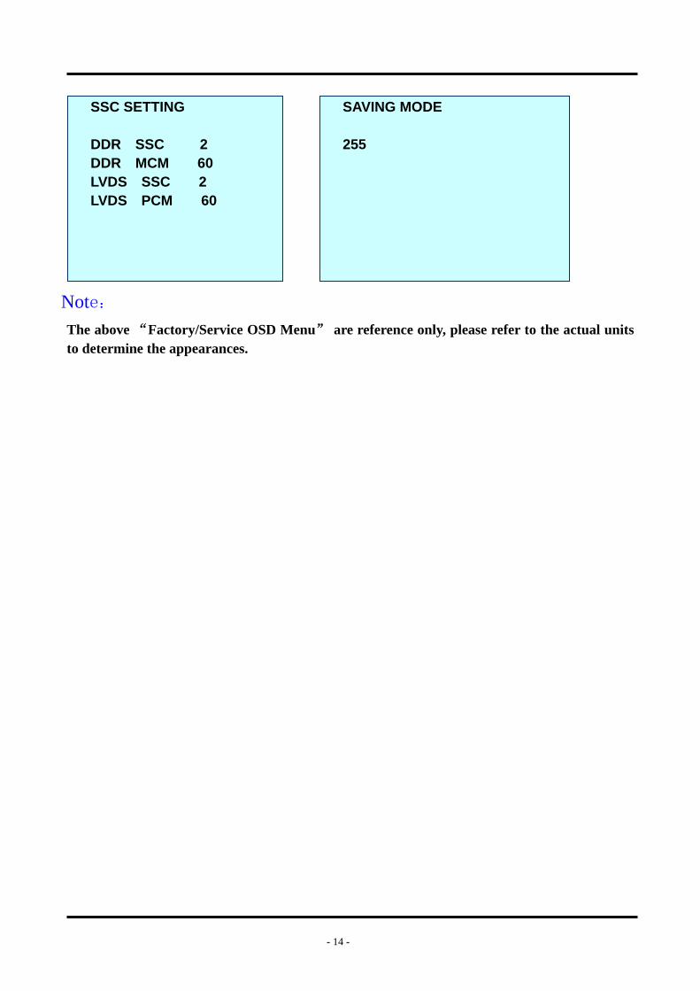
DESIGN MENU PICTURE MODE SOUND MODE PICTURE CURVE AUDIO CURVE SSC SETTING SAVING MODE
- 14 -
Note:
The above “Factory/Service OSD Menu” are reference only, please refer to the actual units to determine the appearances.
SAVING MODE 255
SSC SETTING DDR SSC 2 DDR MCM 60 LVDS SSC 2 LVDS PCM 60

- 15 -
3. Software Upgrading
Before upgrading, read the following.
1、Before upgrading,Write down the ADC Calibration values of the channel of VGA and component。
2、Upgrade the software. 3、To clear the EEPROM . A Select the item “Clear Unprotected”. B Press VOL+ button to clear the EEPROM data. C Close the OSD menu after 5 seconds. D Restart the TV. 4 Write the ADC Calibration values copied just now into the the channels of VGA and
component. 5、After the operation above all, necessarily, Renew search the channels for the users.
3.1 Get ready for upgrading
The software is upgraded by a burning tool- ISP_TOOL4.0.9, which can burn the program file“*.bin” to the main board of the unit
3.1.1 Install the ISP_TOOL4.0.9-------only for the first time update. 1、 Port Setting:

- 16 -
Choose “system”option from the “control panel”
Click the “system” icon as the following
Choose the “hardware” option from the dialog window
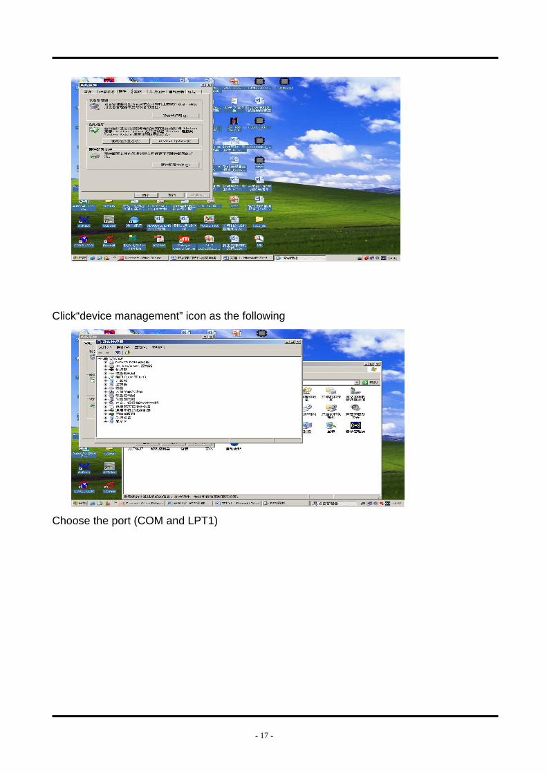
- 17 -
Click“device management” icon as the following
Choose the port (COM and LPT1)
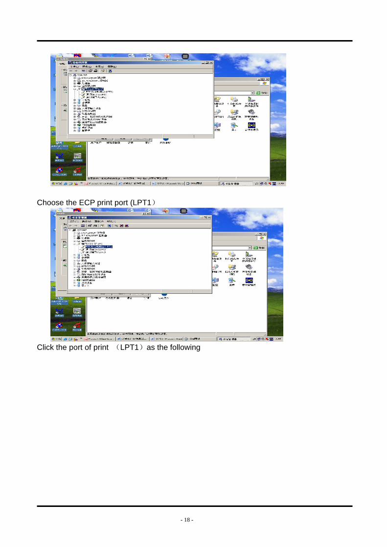
- 18 -
Choose the ECP print port (LPT1)
Click the port of print (LPT1)as the following

- 19 -
Choose “port setting”option as the following

- 20 -
2、 Find the folder where the ISP_TOOL4.0.9 lies in. There are three folders/files in this folder together. DLPORTIO.dll and FTD2XX.DLL must be in the same folder
Double click the ISP_TOOL4.0.9 icon, and then a dialog window will show as below.
- 21 -
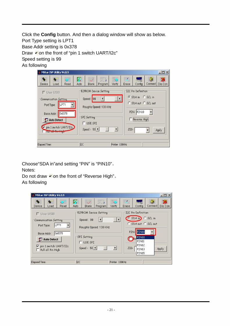
Click the Config button. And then a dialog window will show as below. Port Type setting is LPT1 Base Addr setting is 0x378 Draw on the front of “pin 1 switch UART/I2c” Speed setting is 99 As following
Choose“SDA in”and setting “PIN” is “PIN10”。 Notes: Do not draw on the front of “Reverse High”。 As following

- 22 -
Choose “SCL in”and setting “PIN” is “PIN11”。 Notes: Do not draw on the front of “Reverse High”。 As following
Choose “SDA out”and setting “PIN” is “PIN4” Notes: Draw on the front of “Reverse High”。 As following。
Choose “SCL out”and setting “PIN” is “PIN2” Notes: Draw on the front of “Reverse High” As following

- 23 -
After having finished all above, clicking the “Apply ”button to complete the configuration。
3.1.2 Hardware connecting
You can update the software through a special tool (as following)
Connect the Debug board to the TV use VGA interface, the other parallel port to the

- 24 -
computer, just as the following。

- 25 -
3.2 Upgrading with the ISP_TOOL4.0.9
3.2.1 Double click the ISP_TOOL4.0.9 icon and a dialog window will show as following。
Click the“Read ”button。

- 26 -
Choose the update file from the folder。
- 27 -
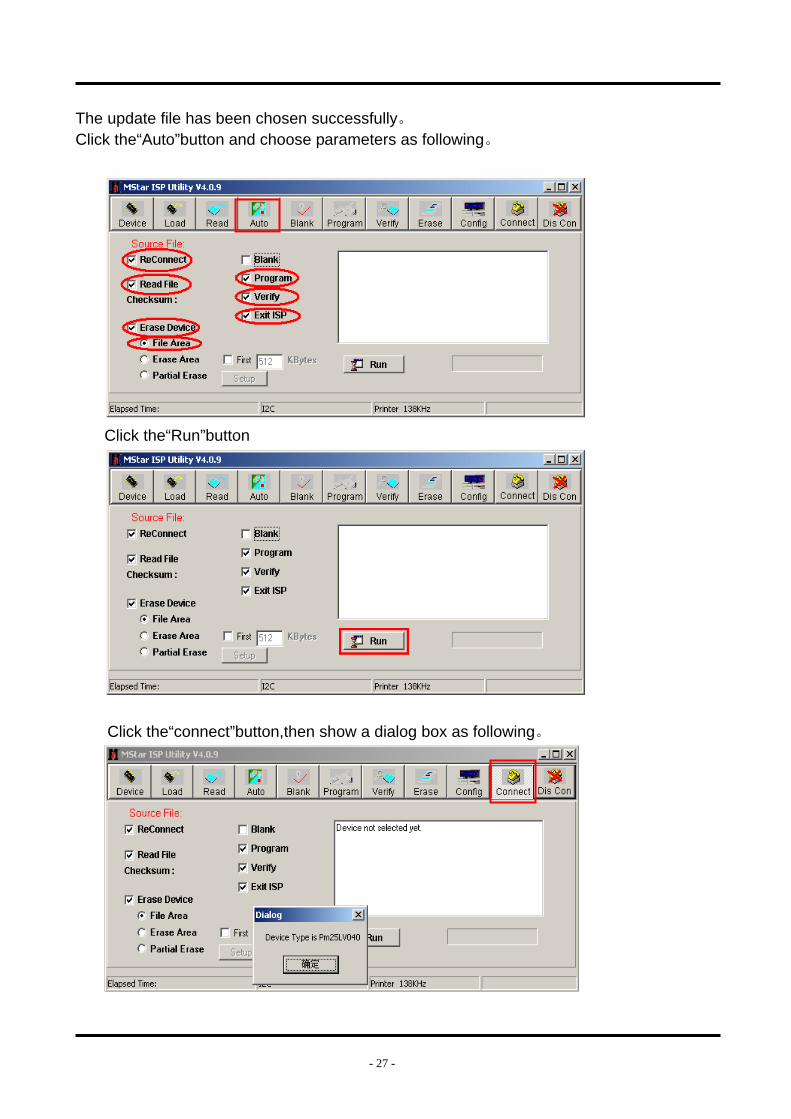
The update file has been chosen successfully。 Click the“Auto”button and choose parameters as following。
Click the“Run”button
Click the“connect”button,then show a dialog box as following。
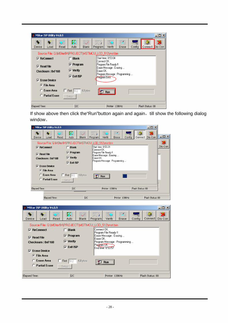
- 28 -
If show above then click the“Run”button again and again,till show the following dialog window。

- 29 -
The above appears on the screen-the word “program ok”shows in the information displaying window,indicating upgrading is over。
3.2.2 After the update is over. Must Confirm the software Version in the Version Menu. If the update is successful, enter Factory Init Menu and select “Clear Unprotectly” a. Press VOL+ button to clear the EEPROM data. b. When the “Clear Unprotectly ” button becomes white, turn off the power. c. Restart the TV.
3.3 USB Software upgrading
3.3.1、Copy the Updating software to the USB root directory, the software named *.bin. for example the TV LCD19W58AM(30) named LCD19W58AM.bin. If the TV has internet function, Insert the USB disk to the interface nearly the Tuner.
- 30 -
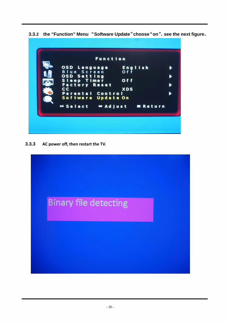
3.3.2 the “Function” Menu “Software Update”choose“on”,see the next figure。
3.3.3 AC power off, then restart the TV.

- 31 -

- 32 -
3.3.4 After update success, AC power off, and restart the TV. If only appear the figure:“Binary file detecting”,the last three figures not. Please modify the
name of sotrware.
3.3.5、 After the update is over. Must confirm the software Version in the Version Menu. If the update is successful, enter Factory Init Menu and select “Clear Unprotectly” d. Press VOL+ button to clear the EEPROM data. e. When the “Clear Unprotectly ” button becomes white, turn off the power. f. Restart the TV.
- 33 -
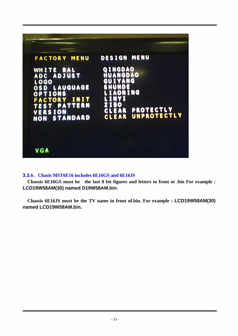
3.3.6、Chasis MST6E16 includes 6E16GS and 6E16JS Chassis 6E16GS must be the last 8 bit figures and letters in front ot .bin For example :
LCD19W58AM(30) named D19W58AM.bin.
Chassis 6E16JS must be the TV name in front of.bin. For example : LCD19W58AM(30) named LCD19W58AM.bin.

- 34 -
4. Circuit instruction
4.1 Main board Power assign and block diagram
Power assign:
The Powerd only has 12V output ,other voltages are converted from 12V.
a. 5Vstb is converted by U10 from 12V,5VAIN and +5V_USB are converted by U7 from 5Vstb.
b. +3.3Vstb that standby power supply for main IC (U41)、Flash (U42)、EEPROM (U43)、HDCP EEPROM
(U21)、Key is converted by 5Vstb from U5.
c. U28 and U30 power supply from 5VAIN
d. +3.3AVDD supply power for main is converted by U6 from 5VAIN; +2.6VM supply power for DDR is
converted by U8 from 5VAIN; VCC-1.26V supply power for main IC(core voltage) is converted by U9
from 5VAIN;
e +12V supply power for audio amplify is converted by U6 from +12V_IN; 5V-IN supply power for Tuner
is converted by U24from +12V_IN;
f VCC-Panel supply power for Panel is converted by U4 from 5VAIN or +12V_IN
Block diagram:
- 35 -
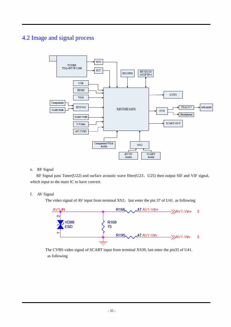
4.2 Image and signal process
e. RF Signal
RF Signal pass Tuner(U22) and surface acoustic wave filter(U23、U25) then output SIF and VIF signal,
which input to the main IC to have convert.
f. AV Signal
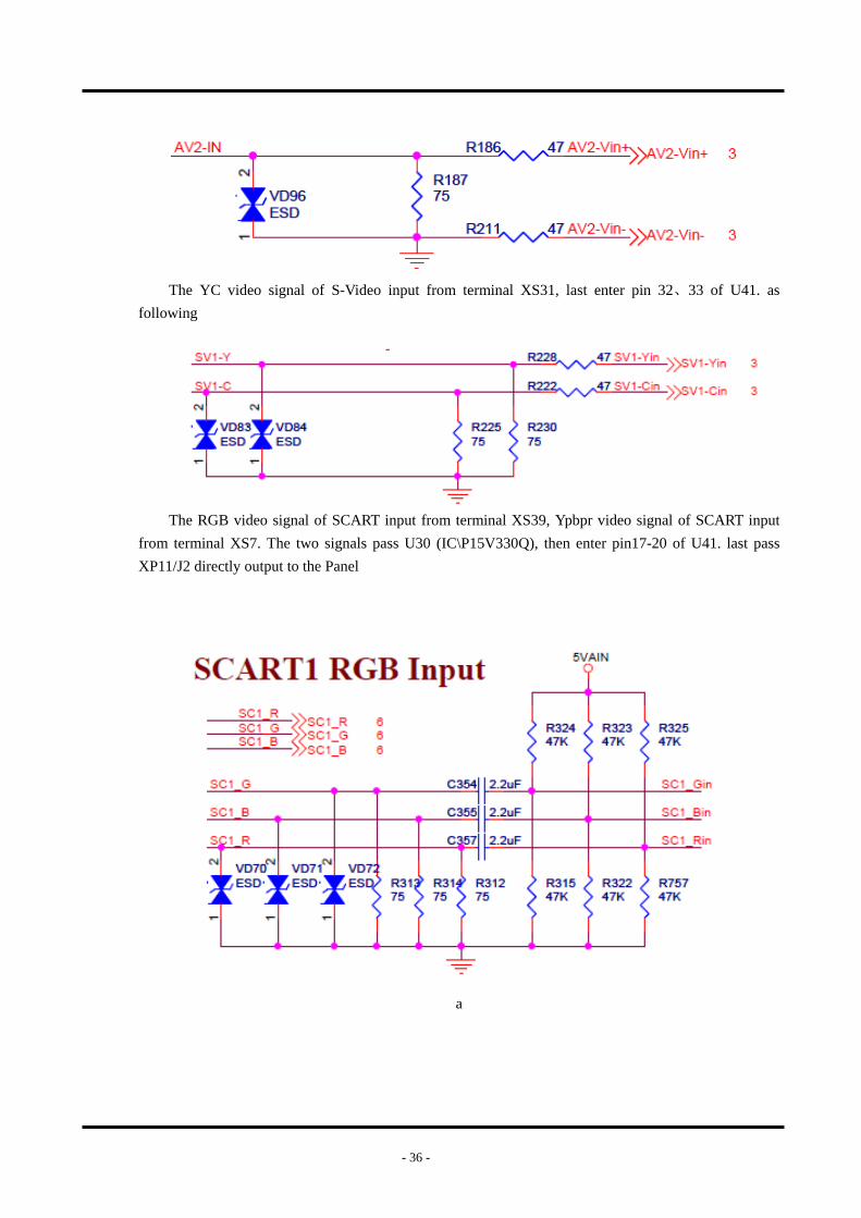
The video signal of AV input from terminal XS2,last enter the pin 37 of U41. as following
The CVBS video signal of SCART input from terminal XS39, last enter the pin35 of U41.
as following
- 36 -
The YC video signal of S-Video input from terminal XS31, last enter pin 32、33 of U41. as
following
The RGB video signal of SCART input from terminal XS39, Ypbpr video signal of SCART input
from terminal XS7. The two signals pass U30 (IC\P15V330Q), then enter pin17-20 of U41. last pass
XP11/J2 directly output to the Panel
a

- 37 -
b
PC(VGA)signal input from Terminal XS39, after having converted,. last enter the pin 22、24、
25、26 of U41.
Audio signal of HDMI and USB directly input IC U41.
Output of Scart (owning to have CANAL+ function , only output RF Signal)which by Pin 40 of
U41, As the following amplified circuit.. Output from terminal XS39.
g. Audio Signal (except HDMI and USB)
Audio Signal of TV is that the SIF signal pass through Tuner(U22) and surface acoustic wave
filter(U23、U25) was converted by U41.

- 38 -
Audio XS7(YPbPr and VGA mutual the channel) Audio XS2 (AV and SV mutual the channel)
2. Control Process:
The Power only has 12V output ,other voltages are converted from 12V. U4 and U7 can interrupt other
voltages while standby, only reserve standby 5V. as following. When TV Power on , Standby Signal is High
level, 5VAIN Power suppluy normally ; When TV standby , the U7 tuner switch is shut off , 5VAIN Power
suppluy is low.
+12V standby signal control as similar as +5V

- 39 -
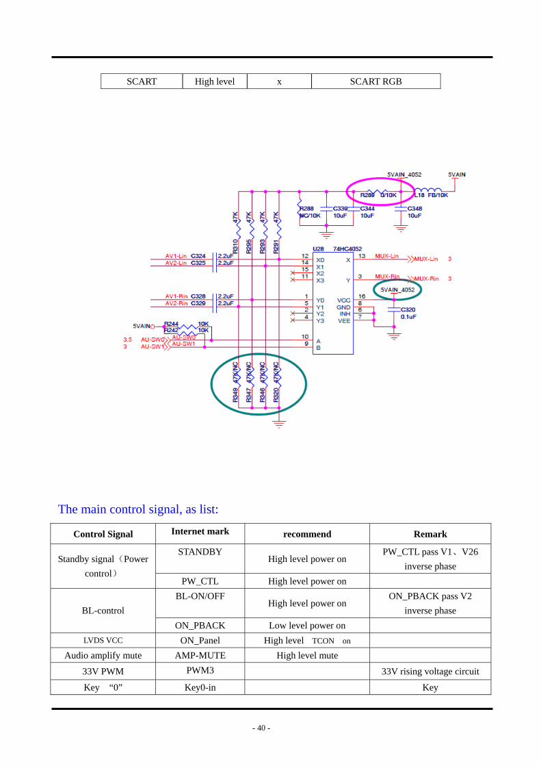
The video input signal of SCART RGB and Component was converted by U30, controlled by AU-SW0
signal. According current signal choose one channel output from 4、7、9 of U30
The control method as following:
Current channel AU-SW0 Switch output signal
Component Low level Component YPbPr
SCART High level SCART RGB
The audio input signal of SCART and AV was converted by U28, controlled by AU-SW0、AU-SW1
signal. According current signal choose one channel output from 3、13 of U U28
The control method as following:
Current channel AU-SW0 AU-SW1 Switch output signal
AV/SV Low level x AV/SV L/R
- 40 -
SCART High level x SCART RGB
The main control signal, as list:
Control Signal Internet mark recommend Remark
STANDBY High level power on
PW_CTL pass V1、V26
inverse phase Standby signal(Power
control) PW_CTL High level power on
BL-ON/OFF High level power on
ON_PBACK pass V2
inverse phase BL-control
ON_PBACK Low level power on
LVDS VCC ON_Panel High level TCON on
Audio amplify mute AMP-MUTE High level mute
33V PWM PWM3 33V rising voltage circuit
Key “0” Key0-in Key
- 41 -
Key “1” Key1-in Key
Remote control signal IR-SYNC IR
4.3 The main IC description
74HC4052D:

- 42 -

- 43 -
AOZ1021
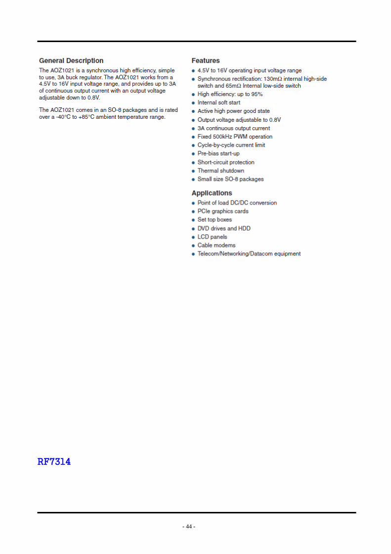
- 44 -
RF7314
- 45 -

- 46 -
MP1482
- 47 -
TPA1517

- 48 -

- 49 -
4.4 Troubleshooting
4.4.1 Troubleshooting for Remote Control
Remote control does not work
Try new batteries
Replace RC
Check IR receiver
Change Led & IR board
Change Led & IR cable
Replace main board
Replace battery
Replace remote control
Replace Led & IR BD
Replace Led & IR cable
YES
YES
NO
YES
NO
YES
NO
- 50 -
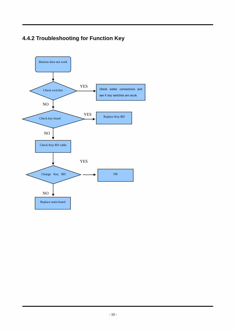
4.4.2 Troubleshooting for Function Key
Buttons does not work
Check switches
Check key board
Check Key BD cable
Change Key BD
Replace main board
Check solder connections and
see if any switches are stuck.
Replace Key BD
OK
YES
YES
NO
YES
NO
NO

- 51 -
4.4.3 TV won’t Power On
Make Sure Power
source is live
Replace
Power Cord
Check/replace IR
BD or Keypad
PCA
TV won’t power on
Is LED
light?
NO
YES
Check Power
Output
YES
NO
Check Power
Cord
Only
one works
Replace Main
BD
Try Power on by
RC and Button
Neither
works Both
Work
Power on OK YES
NO
Replace Power BD
YES
NO
RED BLUE
Panel Bright
NO
Replace Main BD
NO
YES Check signal
Source
YES
NO
YES
Replace Panel
(to contact Hisense tech support.)
OK
- 52 -
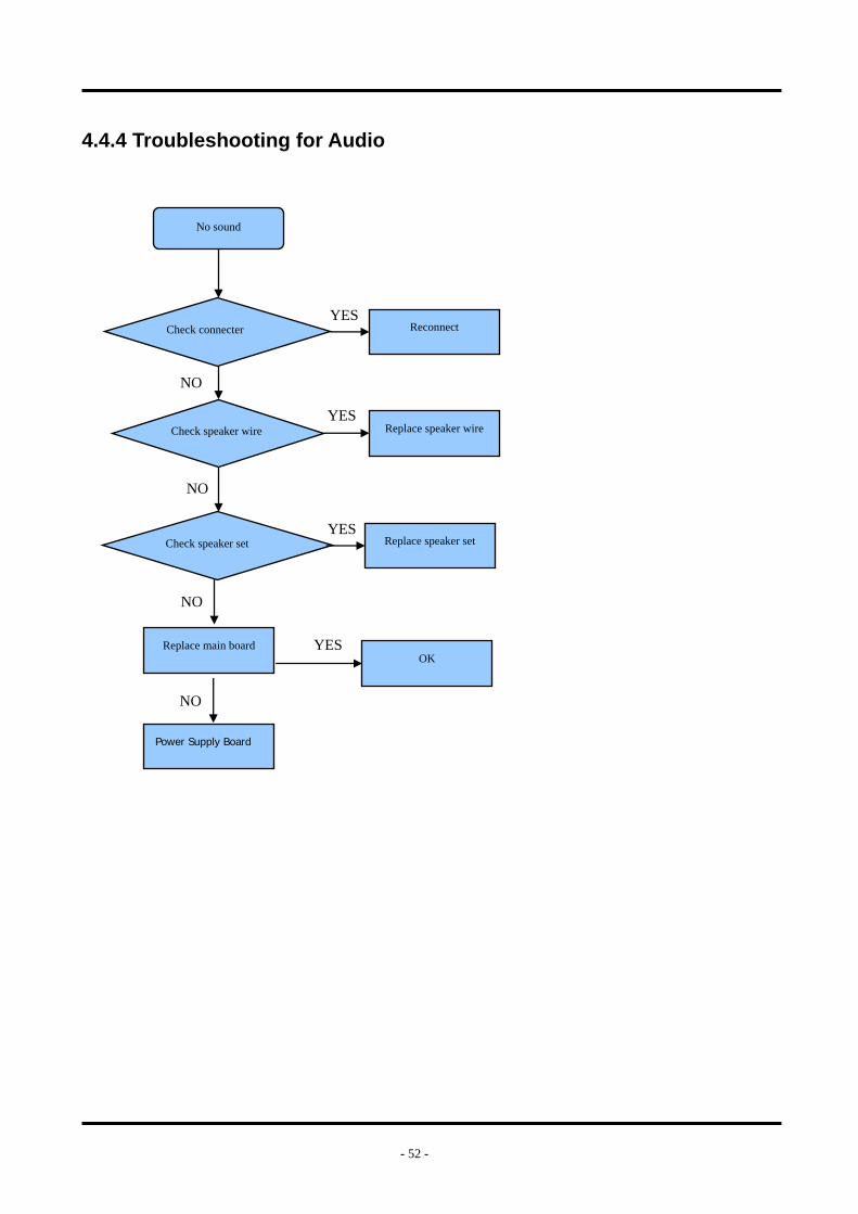
4.4.4 Troubleshooting for Audio
No sound
Check connecter
Check speaker wire
Replace main board
Reconnect
Replace speaker wire
YES
YES
NO
NO
Check speaker set Replace speaker set YES
NO
OK YES
NO
Power Supply Board

- 53 -
4.4.5 Troubleshooting for TV/VGA/HDMI input
No picture on the screen
Check Signal Source
Check connect
Check cable
Replace main board
Make sure signal
source is available
Reconnect
Replace cable
NO
YES
YES
NO
NO
- 54 -
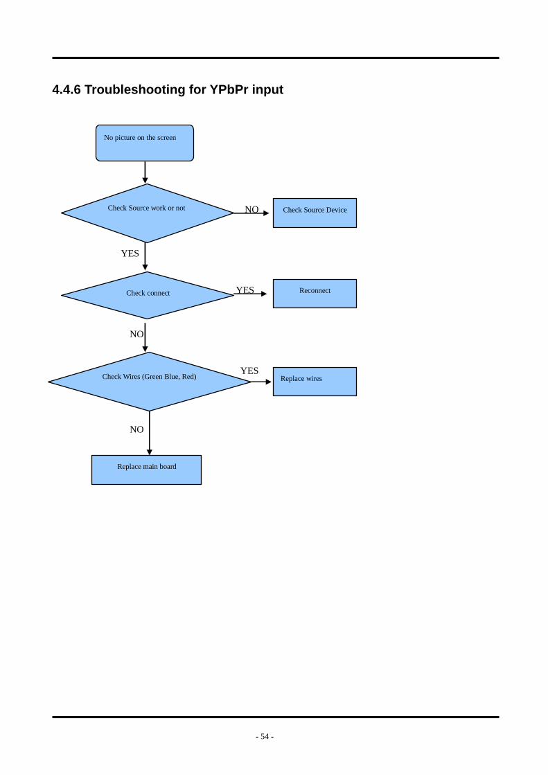
4.4.6 Troubleshooting for YPbPr input
No picture on the screen
Check Source work or not
Check connect
Check Wires (Green Blue, Red)
Replace main board
Check Source Device
Reconnect
Replace wires
NO
YES
YES
NO
YES
NO
- 55 -
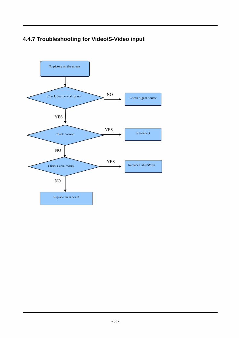
4.4.7 Troubleshooting for Video/S-Video input
No picture on the screen
Check Source work or not
Check connect
Check Cable/ Wires
Replace main board
Check Signal Source
Reconnect
Replace Cable/Wires
NO
YES
YES
NO
YES
NO

- 56 -
5. Schematic circuit diagram
5
5
4
4
3
3
2
2
1
1
D D
C C
B B
A A
2222
12v
ON/OFF
DIM
16
A
DIMON/OFF
12v
16
A
AC1 AC2
AC1 AC2
A
Title
Size Document Number Rev
Date: Sheet of
DCustom
Thursday, September 02, 2010
<Doc>
<Title>
1 1
Title
Size Document Number Rev
Date: Sheet of
DCustom
Thursday, September 02, 2010
<Doc>
<Title>
1 1
Title
Size Document Number Rev
Date: Sheet of
DCustom
Thursday, September 02, 2010
<Doc>
<Title>
1 1
M2
MARK
M2
MARK
C804CAP-HXC804CAP-HX
R834 100KR834 100K
R808
0
R808
0
VD8174148VD8174148
12
R8473M3R8473M3
R87710KR87710K
T802
TRANSFORMER-8-HX
T802
TRANSFORMER-8-HX
1
82
3
7
6
5
4
C8
59
C8
59
VD
81
6
VD
-KG
-HX
VD
81
6
VD
-KG
-HX
12
C856C856
C824105C824105
C814
25V 2200u
C814
25V 2200u
VD807VD807
12
C842 561C842 561
C803CAP-HX
C803CAP-HX
R88122KR88122K
H803H803
1
R81410KR81410K
R812 75RR812 75R
R818R818
C889
104
C889
104
R8900R8900
F801
FUSE-HX
F801
FUSE-HX R801680KR801680K
R862560RR862560R
VD805VD805
12
C812
CAP-HX
C812
CAP-HX
VD801VD801
12
W822W822
R828 1KR828 1K
W812W812
C838
10P
C838
10PR889560RR889560R
C8114.7uFC8114.7uF
VD835VD83512
R8643K9R8643K9
R8313K9R8313K9
R806R806
C886
CAP-HX
C886
CAP-HX
C896
225
C896
225
R886 56RR886 56R
C849104C849104
VD8374148VD8374148
12
R891100RR891100R
C816104C816104
W818W818
L801
L2-EMC-HX
L801
L2-EMC-HX1 2
34
C892103C892103
C80822uFC80822uF
C843 561C843 561
C818104
C818104
W817W817
N805ao4616 N805ao4616
S11
G12
S23
G24
D2_75
D26
D1_67
D18
W813W813
C887
CAP-HX
C887
CAP-HX
N807ao4616 N807ao4616
S11
G12
S23
G24
D2_75
D26
D1_67
D18
R876 10KR876 10K
R887 120RR887 120R
QR804QR804123
R8261KR8261K
W819W819
R8220.47RR8220.47R
R82715KR82715K
VZ812VZ812
12
R8303K9R8303K9
XP808XP808
1234
R882 56RR882 56R
R8930R8930
R8881K5R8881K5
C848105C848105
C919103C919103
R86722KR86722K
C822 104C822 104
C835 561C835 561
V8082907V8082907
3
1
2
R815680RR815680R
VD808VD8081
2
R838100KR838100K
R823NAR823NA
R804R804
T803T803
561
0
7
8
9
3
2
14
C832 224C832 224
R85510K
R85510K
R856 36KR856 36K
VD833VD833
1 2
R865
680K
R865
680K
V8182222
V8182222
1
23
C802C802
C839
10P
C839
10P
C8
20
C8
20
C825
104
C825
104
T801
S-ER-3534-HX
T801
S-ER-3534-HX
1
23
12111098
6 7
45
H802H802
1
VD8154148VD8154148
12
V801V801
1
23
VD812VD8121
23
R883 120RR883 120R
R821100KR821100K
V8072222V8072222
1
23
M3
MARK
M3
MARK
C826103/1KVC826103/1KV
VD836 4148VD836 4148
1 2
C8
07
C8
07
VD804VD804
12
R86310KR86310K
RT801RT801
V819
2907
V819
2907
3
1
2
W801W801
R807R807
R824
270K
R824
270K
R809
0
R809
0
R8540R8540
C8
19
C8
19
VD840VD840
12
C873CAP-HX
C873CAP-HX
R858 680R858 680
VD834VD834
12
VD803VD803
12
R816270K
R816270K
V809
2907
V809
2907
3
1
2
C888
104
C888
104
V804
2907
V804
29073
1
2
C890CAP-HXC890CAP-HX
C806C806
R83568KR83568K
R802680KR802680K
QR803QR803123
R88522KR88522K
R894 0R894 0
R848
33K
R848
33K
W814W814
R836 2KR836 2K
C817
104
C817
104
C828105C828105
R873 10KR873 10K
V803V8031
23
R880 10KR880 10K
VD802VD802
12
M1
MARK
M1
MARK
W820W820
C847 102C847 102
R841100KR841100K
V8202222V8202222
1
23
C830561C830561
R90020KR90020K
R870 680R870 680
QR801QR801
1
R842
270K
R842
270K
N806KA7500C N806KA7500C
+IN11
-IN
12
FB
3
DT
4
CT
5
RT
6G
ND
7
C1
8
E1
9
E2
10
C2
11
VC
C1
2
OC
13
VR
EF
14
-IN
21
5+
IN2
16
N802TL431
N802TL431
1
23
R8962.2KR8962.2K
VD806VD806
12
R805 10RR805 10R
C801C801
R899
0R
R899
0R
W815W815
V8212655V8212655
1
2 3
VD852VD852
12
3
R829270KR829270K
XP805XP805
123456
VD832VD83212
R87424KR87424K
VD811VD811
12
R85710K
R85710K
N803
PC817
N803
PC817
1
23
4
R859 680R859 680
R845300KR845300K
C858C858
R868
680K
R868
680K
C809331C809331
XP801XP801
12
R852120KR852120K
W821W821
RV801RV801
N801
OB2269
N801
OB2269
GN
D1
FB2
Vin
_4
3
RI4
RT5
Sense_76
VDD7
Gate_68
R892 0R892 0
R872 680R872 680
VD8414148VD8414148
1 2
VD809VD809
12
R843
270K
R843
270K
QR802QR8021
R849 NAR849 NA
R897 0RR897 0R
R811 47RR811 47R
R833 100KR833 100K
C813
25V 2200u
C813
25V 2200u C81525V 470uC81525V 470u
L803
L-HX
L803
L-HX
XP807XP807
1234
R84618KR84618K
R832 100KR832 100K
R817R817
R837 100KR837 100K
R840R-HXR840R-HX
C8
21
C8
21
R875 10KR875 10KR89820KR89820K
C836
10P
C836
10P
R87920K
R87920K
R803680KR803680K
C823
104
C823
104
R825
1K
R825
1K
L802
L2-EMC-HX
L802
L2-EMC-HX1 2
34
C850104C850104
C810C810
R844
680K
R844
680K
C837
10P
C837
10P
V8057002V805
70021
23
VD831VD831
12
R8841K5R8841K5
R853 100KR853 100K
C834 561C834 561
C831101C831101

5
5
4
4
3
3
2
2
1
1
D D
C C
B B
A A
HIGH NORMALLOW STANDBY
HIGH NORMALLOW STANDBY
Note: 1.Left C6 NC if want output PWM puls;2.V3-PWM调光,3904偶尔质量问题导致PWM无法实现,后续新板建议使用1815。
TO Inverter Board
STANDBY
BL-ON/OFFBL-ADJUSTBL-ADJUST
PW_CTL
STANDBY
ON_PANEL
BL-ADJUST
BL-ON/OFF
PW_CTLSTANDBY
5VAIN
+5V_USB
5Vstb
5Vstb
5Vstb
+12V_IN
+12V_IN 5Vstb
+12V+12V_IN
VCC-Panel
+12V_IN
5VAIN
5Vstb
5VAIN
5Vstb
ON_USB13
PW_CTL 3
ON_PANEL3
PWMB3
ON_PBACK3
STANDBY3
Title
Size Document Number Rev
Date: Sheet of
MST6E16 A
System Power
A4
1 9Thursday, July 23, 2009
Title
Size Document Number Rev
Date: Sheet of
MST6E16 A
System Power
A4
1 9Thursday, July 23, 2009
Title
Size Document Number Rev
Date: Sheet of
MST6E16 A
System Power
A4
1 9Thursday, July 23, 2009
C1480.1uFC1480.1uF
R37 4.7KR37 4.7K
C9
NC
/0.1
uF
C9
NC
/0.1
uF
U4 AO4801U4 AO4801
S11
G12
S23
G24
D18
D17
D26
D25
V113904V113904
CA4
22
0u
F/1
6V
CA4
22
0u
F/1
6V
V23904V2
39041
23
R47622KR47622K
C288
0.1
uF
C288
0.1
uF
R34010KR34010K
C81uFC81uF
R39 NCR39 NC
V33904/NCV33904/NC
1
23
L17 15uHL17 15uH
V63904V63904
U7 AO4801U7 AO4801
S11
G12
S23
G24
D18
D17
D26
D25
L65 FBL65 FB
R1122KR1122K
R72 4.7KR72 4.7K
CA2
22
0u
F/2
5V
CA2
22
0u
F/2
5V
R4
NC/10K
R4
NC/10K
R21 22KR21 22K
L3 BLM31PGL3 BLM31PG
V43904V43904
1
23
C1460.1uFC1460.1uF
R6 4.7KR6 4.7K
L1 BLM31PGL1 BLM31PG
C289
NC
C289
NC
F1 1.5AF1 1.5A
AOZ1021
U10
AOZ1021
U10
VIN2
FB4 AGND3
EN6
LX281
PGNDLX1
7
COMP5
R34 4.7KR34 4.7K
C141uFC141uF
C345
10
uF
C345
10
uF
C17
22
uF
C17
22
uF
L64 FBL64 FB
R33 10KR33 10K
R2010K/NCR20
10K/NC
C70.1uFC70.1uF
R71 10KR71 10K
R203
4.7K
R203
4.7K
C181uFC181uF
R183 100R183 100
V263904/NC
V263904/NC
1
23
+CA5
100uF/16V+CA5
100uF/16V
R8
4.7K/NC
R8
4.7K/NC
C1470.1uFC1470.1uF
R45
10K
R45
10K
C286
0.1
uF
C286
0.1
uF
C290
NC
C290
NC
R34252.3KR34252.3K
C101uFC101uF
R46 4.7KR46 4.7K
R339100KR339100K
R54 10KR54 10K
XP26
Power
XP26
Power
112233445566
R36 10KR36 10K
R294.7KR294.7K
R350RR350R
C62.2uF/0R
C62.2uF/0R
V1043904V1043904
1
23
R16
22K
R16
22K
C16
NC
/22
uF
C16
NC
/22
uF
C13
NC
/0.1
uF
C13
NC
/0.1
uF
R38 NC/0R38 NC/0
V5NC/3904V5NC/3904
1
23
C19
22
uF
C19
22
uF
R7
4.7K
R7
4.7K
C291
2.2nF
C291
2.2nF
R434.7K/NC
R434.7K/NC
R47422KR47422K
+CA9
NC
/10
0u
F+CA9
NC
/10
0u
F
C50.1uFC50.1uF
R18 1K/NCR18 1K/NC
V13904V13904
1
23
R1210KR1210K
+CA6
10
0u
F/1
6V
+CA6
10
0u
F/1
6V
C285
2.2nF
C285
2.2nF
R1784.7KR1784.7K
main board pcb 1861

5
5
4
4
3
3
2
2
1
1
D D
C C
B B
A A
+3.3Vstb forVDD_MPLL
+3.3Vstb for VDDP_PM
Pin5, Pin27, Pin39,Pin205
+3.3Vstb for AVDD_33
262mA 10mA
Pin45
For standby read EDID
Pin56、Pin61
30mA
?mAPin47
?mAPin54
?mAPin141
MST6E16GS L48=FB,U6=NCMST6E16JS L48=NC,U6=1117
Close To IC Pin
2.6V for MST6E16 and DDRAM
+2.6V for MST6E16
30mA
Pin91, Pin107,Pin111, Pin117, Pin122,Pin128,Pin133
FOR use DDR,+2.6VM must be 2.6V
1.26V
3.3_Stb1084
3.3V
2.6V_DDR1117
111712V
DC/DCAOZ1021
5V USB
5V_Stb
5V PanelPMOS
PMOS
5V Tuner7805
12V Audio(Scart, Phone)
33V_TunerPWM
5VA
12V 预中放PMOS
DC/DCMPS1482
12V Amplifier
PMOS
Vcc 1.26V for MST6E16 Core power
Pin78, Pin89, Pin151,Pin171, Pin202
注意:L7电流要大,直流电阻要小,保证VDDC到MST6E16GS的电压在1.26V
1.32V>VDDC>1.26V,最好在ICPIN脚有1.26V以上
MST Core Voltage need to set 1.28V
Low ESR
600mA
Pin145,Pin164
Close To IC Pin
Pin1084mA
Pin76, Pin167, Pin184, Pin198
PWM1
5Vstb
+3.3Vstb
+3.3Vstb AVDD_MPLL_PMAVDD_33_PM+3.3Vstb AVDD_RXS AVDD_RXV
AVDD_USB
5VAIN
+3.3AVDD +3.3Vstb
+3.3AVDD
+3.3AVDD +3.3AVDD
+2.6VM
+2.6MVDD+2.6VM
5VAIN
VDDCVCC-1.26V
VCC-1.26V
5Vstb
5VAIN
+3.3Vstb
VDDP_PM
+3.3AVDD
AVDD_MemPLL AVDD_AU
VDDP
+3.3Vstb
+3.3AVDD
PM_CTL3
Title
Size Document Number Rev
Date: Sheet of
深圳市高新区南区科技南十路国际技术创新研究院C座4楼
TEL:0755-26996895 FAX:0755-26996830
MST6E16 A
Power
A3
2 9Wednesday, January 06, 2010
Title
Size Document Number Rev
Date: Sheet of
深圳市高新区南区科技南十路国际技术创新研究院C座4楼
TEL:0755-26996895 FAX:0755-26996830
MST6E16 A
Power
A3
2 9Wednesday, January 06, 2010
Title
Size Document Number Rev
Date: Sheet of
深圳市高新区南区科技南十路国际技术创新研究院C座4楼
TEL:0755-26996895 FAX:0755-26996830
MST6E16 A
Power
A3
2 9Wednesday, January 06, 2010
+CA46470uF/16V
+CA46470uF/16V
C61
0.1uF
C61
0.1uF
AD
J
OU
T
IN
U8AMS1117-ADJ
AD
J
OU
T
IN
U8AMS1117-ADJ
321
4
C730.1uFC730.1uF
C28
0.1uF
C28
0.1uF
C44
0.1uF
C44
0.1uF
C330.1uF
C330.1uF
C66
0.1uF
C66
0.1uF
R27013K_1%R27013K_1%
L15 FBL15 FB
C2020.1uFC2020.1uF
R73220R73220
C1040.1uFC1040.1uF
R271NCR271NC
C27
0.1uF
C27
0.1uF
C42
0.1uF
C42
0.1uF
C700.1uFC700.1uF
C510.1uFC510.1uF
L19 FBL19 FB
C38822uF
C38822uF
C2870.1uFC2870.1uF
L14 NC/FBL14 NC/FB
L8 10uH 2.5AL8 10uH 2.5A
R306 100K/NCR306 100K/NC
C57
0.1uF
C57
0.1uF
C3802.2uFC3802.2uF
C230.1uFC230.1uF
C3962.2uFC3962.2uF
OU
T
AD
J
IN
U51084-3.3
OU
T
AD
J
IN
U51084-3.3
321
4
MP1482U9MP1482U9
COMP6
SW3
FB5
SS8
IN2
GND4
EN7
BS1
C35
0.1uF
C35
0.1uF
C43
0.1uF
C43
0.1uF
C29610uFC29610uF
L48 FBL48 FB
C240.1uFC240.1uF
C30
0.1uF
C30
0.1uF
CA94100uF/16VCA94100uF/16V
C990.1uFC990.1uF
C362NCC362NC
C3862.2uFC3862.2uF
C36
0.1uF
C36
0.1uF
C470.1uFC470.1uF
C29
0.1uF
C29
0.1uF
L21 NCL21 NC
C37
0.1uF
C37
0.1uF
C970.1uFC970.1uF
C68
0.1uF
C68
0.1uF
L16 NCL16 NC
R304 NC/100R304 NC/100 C2840.1uFC2840.1uF
C38
0.1uF
C38
0.1uF
C880.1uFC880.1uF
C69
0.1uF
C69
0.1uF
C620.1uFC620.1uF
C26
0.1uF
C26
0.1uF
C3842.2uFC3842.2uF
L51 FBL51 FB
C3602.2uFC3602.2uF
C670.1uFC670.1uF
C2980.1uFC2980.1uF
C3523.3nFC3523.3nF
C3702.2uFC3702.2uF
C3742.2uFC3742.2uF
C340.1uFC340.1uF
+CA79
100uF/16V
+CA79
100uF/16V
L50 FBL50 FB
C45010nFC45010nF
C210.1uFC210.1uF
C250.1uFC250.1uF
+CA7100uF/16V
+CA7100uF/16V
R74200R74200
C890.1uFC890.1uF
R2695.1K_1%R2695.1K_1%
C580.1uFC580.1uF C395
2.2uFC3952.2uF
C39
0.1uF
C39
0.1uF
R2922.2KR2922.2K
C38522uF
C38522uF
L13 FBL13 FB
C3712.2uFC3712.2uF C45
0.1uF
C45
0.1uF
AD
J
OU
T
IN
U6NC/AMS1117-3.3
AD
J
OU
T
IN
U6NC/AMS1117-3.3
321
4
main board pcb 1861
5
5
4
4
3
3
2
2
1
1
D D
C C
B B
A A
Y,Pb
,Pr
INPU
TAU
DIO
INPU
T
PANELINTERFACE
CL=20pf of XTAL
VIDE
OIN
PUT
AUDI
OOUT
PUT
Please closeto chip.
WARNING !!!
HDM
I IN
PUT
Mode SelectionPWM1PWM0=10
Not 5V-tolerant
FOR U12,+2.6V_DMQ,+2.6V_DMC must be 2.6V
Not 5V-tolerant
PWM0 PWM10 0 --> serial bus0 1 --> direct busx 1 --> internal MCU
(4.75V---5.25V)
VGA
INPU
T
Not 5V-tolerant
GPIO[2:0] Not 5V-tolerant
AD[0-2] Not 5V-tolerant
AD[0-2] Not 5V-tolerant
5V-tolerant
5V-tolerant5V-tolerant5V-tolerant5V-tolerant
5V-tolerant5V-tolerant
SAR0 PM
Flash WP PIN:PWM0,PWM3,SAR3
SDRAM删除
Not 5V-tolerant
LVDS接口、FFC接口屏的SEL分别通过(R300/R303/C438)、(R305/R307/C439)匹配,注意网络不同,C9、C13分别位于两种插座VCC处
PWMB:如果确实需要,优先选择PWM0,便于频率调整;
MST6E16GS:采用R296;MST6E16JS:采用R350;MST6E16GS采用R418、R683MST6E16JS采用R680、R427
AD[0-2] Not 5V-tolerant
SPI_CZ
SPI_CK
SPI_DO
SPI_DIPWM1PWM0
MCU_I2C_SCLMCU_I2C_SDA
MCU_I2C_SCLMCU_I2C_SDA
WP_EEP
WP_FLASHWP_FLASHWP_FLASHWP_FLASH
LED_CTL
CASZ
LDQM
FSVREF
CKEMCLK+MCLK-
DQS1
UDQM
BA0
RASZ
DQS0
WEZ
AR4AR3AR2 AR5
AR6AR1
AR10AR7AR8
AR0
AR11BA1 AR9
FSVREF MVREF
WP_KEY
SAR0
DQM0
MCLKMCLKZDQM1
MDQS0
MDQS1
MCLKEMVREF
MADR0
MADR4
MADR8
MADR2MADR1
MADR6
MADR11
MADR5
MADR10MADR9
MADR7
MADR3
MDATA1
MDATA15
MDATA12
MDATA7
MDATA9
MDATA4
MDATA2MDATA3
MDATA10
MDATA13
MDATA0
MDATA14
MDATA5
MDATA11
MDATA6
MDATA8
BA1
MRASZMCASZMWEZ
BA0
SAR1
SYS_RST
USB1_OC_DET
RXE1-
RXE0-
RXE1+RXE2-RXE2+
RXE0+
RXEC+RXEC-
RXE3+RXE3-
RXE4-RXE4+
RXO0-
RXO4+RXO4-
RXOC+
RXO1+RXO2-RXO2+
RXO3+RXO3-
RXOC-
RXO1-RXO0+
DQS0
DQS1
CASZRASZ
WEZ
MCLK-MCLK+
DATA11
DATA13
DATA4
DATA7
DATA1
DATA8
DATA15DATA14
DATA2
DATA5DATA6
DATA9
DATA0
DATA12
DATA3
DATA10
UDQM
AR8
AR0
AR10
AR4
AR9
AR3AR2
AR5
AR1
AR6AR7
AR11
LDQM
CVBSOut
AUVRADN
AUVREFAUVRADP
AUL0AUR0AUL1AUR1
PC-Lin
AUCOM
PC-RinMUX-LinMUX-Rin
LINE_OUT_1LLINE_OUT_1RDAC_OUT_0LDAC_OUT_0R
VR27
SIFM
VIFP
SIFP
VIFM
TAGC
KEY1-inKEY0-in
SP
I_C
KS
DI
SD
OS
CZ
SC
KS
PI_
DI
SP
I_C
ZS
PI_
DO
IR_
SY
NC
USB1_OC_DETLED_Originally
TAGC
VIFPVIFMSIFPSIFM
DATA9
DATA11
DATA8
DATA13DATA14
DATA10
DATA12
DATA15
DATA1
DATA7
DATA2
DATA4DATA3
DATA0
DATA5DATA6
CKE
AV2-Vin-AV2-Vin+
AV1-Vin-AV1-Vin+
CVBS1VCOM1CVBS0VCOM0
Y1SV1-CinSV1-Yin
C1
RIN2PGIN2PSOGIN2BIN2P
Y+SOY
PR+
PB+VCOM3VCOM2
SOGIN1GIN1P
HS_RGB
SOGGIN+
BIN+
RIN+
VS_RGB
RIN1P
BIN1P
REFPREFM
VCLAMP
HDMIA_HPDCTRL
HDMIA-RXC-
HDMIA-DDC-SDA
HDMIA-RX1+
HDMIA-RXC+
HDMIA-DDC-SCL
HDMIA-RX2-
HDMIA-RX0-
HDMIA-RX2+
HDMIA-RX0+
HDMIA_HPDCTRL
HDMIA-RX1-
Power_CTL
AMP-MUTE
USB1_D+USB1_D-
SIF_SWON_PBACK
PW
M2
PW
M3
PW
M1
WP_EEP
AMP-LAMP-R
SC1-LSC1-R
WP_EEPPW_CTLON_PBACKAMP-MUTE
SAR3
AU-SW0AU-SW1
GAIN_SW
GAIN_SWVIF_SW
USB1_D-USB1_D+
RXD0TXD0
SAR3
RXE3-
RXE2-RXEC-
RXE3+
RXE2+RXEC+
RXE0+ RXE0-
RXE4-RXE4+
RXE1+ RXE1-
RXO3+ RXO3-RXO4-
RXO0+RXO1-RXO1+
RXOC+RXO2+ RXO2-
RXO0-
RXOC-
RXO4+
LVDS_SL_L
LVDS_SL_L
LED
KEY1-in
KEY0-in
IR-in
LED_CTL
I2C_SCLI2C_SDAMSDA
MSCL
IR_SYNC
MSCL
SC_FB
SC_FS
MCU_I2C_SCL
MCU_I2C_SDAMCU_I2C_SCL
RXE0-RXE0+
RXE1-
VCC-Panel
RXE1+
VCC-PanelVCC-Panel
RXE2-
VCC-Panel
RXE2+
VCC-Panel
RXEC-RXEC+
RXE3-RXE3+
LVDS_SL_F
I2C_SCL
I2C_SDAMCU_I2C_SDA
RXD0TXD0
PWM1
LVDS_SL_F
PWM2
PW
M0
PWM0 HDMI_CECPWM0
LEDPWM2PWMB
PWMBPWM0
PWM2
LEDLED_Originally
WP_FLASHWP_FLASHWP_FLASHWP_FLASH
ON_PANELON_USB1
PW_CTL
VIF_SW
PW_CTLPower_CTL
PWM1
GAIN_SWVIF_SW
WP_EEP
AMP-MUTEON_PBACK
VCC-Panel1,9
+3.3Vstb
+3.3Vstb
+3.3Vstb
5Vstb
+2.6V_DMQ +2.6MVDD
+2.6V_DMC +2.6V_DMQ
+2.6V_DMQ+2.6V_DMC
AV
DD
_A
U
AVDD_33_PM AV
DD
_Mem
PLL
VDDPVDDC
AV
DD
_US
B
AV
DD
_MP
LL
_P
M
AV
DD
_RX
V
AV
DD
_RX
S
+2.6MVDD
5V-IF
+5V_USB
AVDD_33_PM
+3.3Vstb
+5V_USB
5Vstb
+2.6VM +2.6VM
5Vstb
VDDP_PM
+3.3Vstb
VCC-Panel
VCC-Panel
+3.3Vstb
5Vstb
+3.3Vstb
VCC-Panel
+3.3Vstb
5Vstb
5Vstb
5Vstb+3.3Vstb
+3.3Vstb
+3.3AVDD
5Vstb
+3.3AVDD
CVBSOut6
PC-Lin5PC-Rin5MUX-Lin6MUX-Rin6
TAGC7
VIFP7VIFM7SIFP7SIFM7
AV2-Vin+6AV2-Vin-6
SV1-Cin6SV1-Yin6
PR+5
SOY5Y+5
PB+5
HS_RGB5VS_RGB5BIN+5SOG5GIN+5RIN+5
HDMIA-RXC-4
HDMIA-DDC-SDA4
HDMIA-RX1+4
HDMIA-RXC+4
HDMIA-DDC-SCL4
HDMIA-RX2-4
HDMIA-RX0-4
HDMIA-RX2+4
HDMIA-RX0+4
HDMIA_HPDCTRL4
HDMIA-RX1-4
AMP-MUTE 8
ON_PBACK 1
PWM3 7
AV1-Vin+6AV1-Vin-6
AMP-R8AMP-L8
SC1-L6SC1-R6
SIF_SW 7
TXD05RXD05
AU-SW0 5,6AU-SW1 6
ON_USB1 1ON_PANEL 1
PM_CTL 2
VIF_SW 7
SC_FB6
SC_FS6
GAIN_SW 7
I2C_SDA 7
I2C_SCL 7
HDMI_CEC4
PWMB 1
PWMB 1PW_CTL 1
PW_CTL 1
Title
Size Document Number Rev
Date: Sheet of
MST6E16 A
Main
A2
3 9Wednesday, December 02, 2009
Title
Size Document Number Rev
Date: Sheet of
MST6E16 A
Main
A2
3 9Wednesday, December 02, 2009
Title
Size Document Number Rev
Date: Sheet of
MST6E16 A
Main
A2
3 9Wednesday, December 02, 2009
V182N7002V182N7002
1
32
R42710K/NCR42710K/NC
R386 100R386 100
C25647pFC25647pF
V73906V73906
1
32
R447 NC/0RR447 NC/0R
R683 NC/0R683 NC/0
C363
0.1uF
C363
0.1uF
R350 100R350 100
L5
6N
C/F
BL
56
NC
/FB
R153
22K
R153
22K
C367100pFC367100pF
R379 100R379 100
R462NCR462NC
R428
10K
R428
10K
C141
0.1uF
C141
0.1uF
R449 100R449 100
R456
4.7K
R456
4.7K
R438
4.7K
R438
4.7K R426NCR426NC
C35627pFC35627pF
R40 100R40 100
C123
0.1uF
C123
0.1uF
R388 100R388 100
C152
10nF
C152
10nF
R27 1KR27 1K
R662 NC/100R662 NC/100
R102 NC/4.7KR102 NC/4.7K
R701100KR701100K
C316 47nFC316 47nF
C816 0.1uFC816 0.1uF
C137
0.1uF
C137
0.1uF
R26100KR26100K
R473 4.7KR473 4.7K
R120220R120220
C156 47nFC156 47nF
R171 100R171 100
R290 100R290 100
R454 390_1%R454 390_1%
R299 100R299 100
C8140.1uF
C8140.1uF
XP24Debug1XP24Debug1
1234
R221 100R221 100
C4381uFC4381uF
C3060.1uFC3060.1uF
L5
3N
C/F
BL
53
NC
/FB
R17222KR17222K U43
24C64
U43
24C64
A01
A12
A23
GND4
SDA5SCL6WP7VCC8
C176
10nF
C176
10nF
VD5
INPAQ_EGA
VD5
INPAQ_EGA12
L52 FBL52 FB
C140
0.1uF
C140
0.1uF
R44 100R44 100
R208 150_1%R208 150_1%
R478 910_1%R478 910_1%
R135 4.7KR135 4.7K
C38
7N
C/1
0pF
C38
7N
C/1
0pF
L54 FBL54 FBR666 5.1R666 5.1
C158 47nFC158 47nF
C214 47nFC214 47nF
V172N7002V172N7002
1
32
C139
0.1uF
C139
0.1uF
R294 100R294 100
R149
22K
R149
22K
R435
4.7K
R435
4.7K
Y114.318MHZY114.318MHZ
12
C26327pFC26327pF
R192 100R192 100
C400
0.1uF
C400
0.1uF
R682 NC/0R682 NC/0
R4430RR4430R
R453
4.7K
R453
4.7K
C309 47nFC309 47nF
R42310KR42310K
R158 4.7KR158 4.7K
43
21
56
78RP31
100
43
21
56
78RP31
100
R104 4.7KR104 4.7K
R4461MR4461M
U12 HY5DU281622ET-4U12 HY5DU281622ET-4
A029
A130
A231
A332
A435A536A637A738A839A940
A10/AP28
A1141
DQ02
DQ14
DQ25
DQ37
DQ48
DQ510
DQ611
DQ713
DQ854
DQ956DQ1057
DQ1159DQ1260
DQ1362DQ1463
DQ1565
BA026
BA127
CS24 RAS23 CAS22 WE21 LDM20
UDM47
LDQS16
UDQS51
CKE44CLK45CLK46
MVDD1
MVDD18
MVDD33
VDDQ3
VDDQ9
VDDQ15
VDDQ55
VDDQ61
VSS34
VSS48
VSS66
VSSQ6
VSSQ12
VSSQ58
VSSQ64
VREF49
VSSQ52NC
14
NC17
NC19
NC25 NC
43
NC53
NC50
NC42
C241 22pFC241 22pF
R429
4.7K
R429
4.7K
R103 NC/4.7KR103 NC/4.7K
VD1BAV99VD1BAV99
3
2
1
R5233KR5233K
C142
0.1uF
C142
0.1uF
U41
MST6E16
U41
MST6E16
GN
D28
RXACKP2
GN
D42
RXACKN1
TAGC55
RXA0N3
RXA0P4
AV
DD
_33
39
RXA1N6
RXA1P7
HOTPLUGA10
REXT11
DDCDA_SDA12
DDCDA_SCL13
HSYNC029
VSYNC030
VCLAMP14
REFP15
REFM16
BIN0P22
SOGIN025
GIN0P24
RIN0P26
BIN0M21
BIN1P17 GIN0M23
RIN1P20
AV
DD
_33
27
CVBS432
CVBS333
CVBS234
CVBS135
VCOM136
CVBS037
VCOM038
AV
DD
_33
5
GPIOD0/RXD173GPIOD1/TXD174GPIOD[2]75
VR2746
GN
D53
DQS[1]134
MDATA[15]132
MDATA[14]131
GN
D57
MDATA[12]129
AV
DD
_M
I122
MDATA[11]127
MDATA[10]126
BADR[1]86
GN
D90
AV
DD
_M
I117
MDATA[7]121
MDATA[6]120
MDATA[4]118
AV
DD
_M
I111
MDATA[3]116
MDATA[2]115
MDATA[1]113
MDATA[0]112
DQS[0]110
DQM0109
MVREF139
MCLKE138
MCLKZ136MCLK137
GN
D114
AV
DD
_M
I107
AV
DD
_M
IPLL
108
CASZ92WEZ93
MADR[0]105
MADR[1]104
MADR[2]103
MADR[3]102
MADR[4]101
AV
DD
_M
I91
VD
DC
171
MADR[8]97
SP
I_S
CK
146
ALE/SOFTWARE SDA85
VD
DC
151
SP
I_S
DI
147
SP
I_S
CZ
148
SP
I_S
DO
149
SA
R1
153
SA
R2
154
PW
M0
156
MADR[6]99
VD
DP
184
SA
R3
155
GN
D144
VD
DP
145
PW
M3
166
VD
DC
89
VD
DP
167
LVA3P174LVA3M175LVACKP176LVACKM177LVA2P178LVA2M179LVA1P180LVA1M181LVA0P182LVA0M183
VD
DP
164
INT
162
LVB3P188LVB3M189LVBCKP190LVBCKM191LVB2P192LVB2M193LVB1P194LVB1M195LVB0P196LVB0M197
RDZ//SOFTWARE SCL84
VD
DP
76
RXB1P210
RXB2P213
HOTPLUGB214
VD
DC
78
HW
RE
SE
T169
XO
UT
43
XIN
44
AV
DD
_M
PLL
45
VIFP52
RXA2P9 RXA2N8
PW
M2
165
GPIOM[0]200GPIOM[1]/HDMI_CEC201
GIN1P19 SOGIN118
CVBSOUT041
SIFP49
AV
DD
_33
56
VIFM51
SIFM50
AUVRM58 AUVRP59 AUVAG60
AV
DD
_A
U61
LINE_IN_0L62
LINE_IN_0R63
LINE_IN_1L64
LINE_IN_1R65
AUCOM66
LINE_OUT_3L67
LINE_OUT_3R68
LINE_OUT_1L71
LINE_OUT_1R72
LINE_OUT_2L69
LINE_OUT_2R70
PW
M1
157
SA
R0
152
IRIN
163
GN
D125
GN
D170
GN
D185
GN
D208
WRZ/SPDIFO83
AD[1]80AD[2]81AD[3]/SPDIF IN82
MADR[5]100
MADR[7]98
MADR[9]96
MADR[10]95
MADR[11]94
BADR[0]87RASZ88
MDATA[13]130
MDATA[9]124
MDATA[8]123
MDATA[5]119
LVA4P172LA4M173
LVB4P186LVB4M187
VD
DP
198
GN
D199
RXB2N212
RXBCKN203
RXBCKP204
DQM1135
GP
IOT
[1]/U
SB
_D
RV
VB
US
168
RXB0N206
RXB0P207
RXB1N209 A
VD
D_R
XS
47
AV
DD
_R
XV
54
AV
DD
_M
I128
AV
DD
_M
I133
VD
DC
202
GN
D77
GN
D106
AD[0]79
GN
D150
USB2_REXT140
AV
DD
_U
SB
141
USB20_DM142USB20_DP143
GN
DP
AD
217
GN
D48
AV
DD
_33
205
GN
D211
DDCDB_SDA215
DDCDB_SCL216
VSYNC231
CVBSOUT140
DDCR_SDA158
DDCR_SCL159
DDCA_SDA160
DDCA_SCL161
43
21
56
78RP30
100
43
21
56
78RP30
100
C379
10uF
C379
10uF
C150
1nF
C150
1nF
R389 100R389 100
U42
KH25L1605D
U42
KH25L1605D
CE#1
SO2
WP#3
VSS4
SI5
SCK6
HOLD#7
VDD8
R448 NC/0RR448 NC/0R
R424NCR424NC
C366100pFC366100pF
R308 47R308 47
R217 100R217 100
C439
1uF
C439
1uF
C3130.1uFC3130.1uF
C36
510
0pF
C36
510
0pF
R450 100R450 100
R380 100R380 100
4321
5678
RP19 100
4321
5678
RP19 100
C20710uFC20710uF
C26547pFC26547pF
R661 5.1R661 5.1
R65510KR65510K
R30012KR30012K
R378 100R378 100
R486 22R486 22
R358 47R358 47R664 100R664 100
C122
0.1uF
C122
0.1uF
C435
1uF
C435
1uF
XP15
KEY
KEYXP15
KEY
KEY
1234
R1704.7KR1704.7K
43
21
56
78 RP29
100
43
21
56
78 RP29
100
C3120.1uFC3120.1uF
R30322KR30322K
R65410KR65410K
C3381nFC3381nF
R440 4.7KR440 4.7K
R359 47R359 47
C813
NC
C813
NC
C368
0.1uF
C368
0.1uF
R309 47R309 47
R2642.2KR2642.2K
R479 4.7KR479 4.7K
C335 2.2uFC335 2.2uF
C310 47nFC310 47nFR483 100R483 100
XP11 LVDSXP11 LVDS
VCC2
VCC1
VCC4
VCC3
GND6
GND5
GND8
GND7
LVDS_SL/SCL10
AI/SDA9
BRI_OUT12
BRI_EXT/DIS11
GND14
GND13
TXA0+16
TXA0-15
TXA1+18
TXA1-17
TXA2+20
TXA2-19
TXAC+22
TXAC-21
TXA3+24
TXA3-23
TXA4+26
TXA4-25
GND28
GND27
TXB0+30
TXB0-29
TXB1+32
TXB1-31
TXB2+34
TXB2-33
TXBC+36
TXBC-35
TXB3+38
TXB4+40 TXB3-
37
TXB4-39
R4420RR4420R
R431
4.7K
R431
4.7K
XP4IR&LEDXP4IR&LED
12345678
43
21
56
78 RP40
22R
43
21
56
78 RP40
22R
R207 100R207 100
C317 47nFC317 47nF
C1201nFC1201nF
R452 100R452 100
C135 47nFC135 47nF
R480
4.7K
R480
4.7K
R2662.2KR2662.2K
R30712KR30712K
VD3INP
AQ
_V
PO
RT
VD3INP
AQ
_V
PO
RT
R477 4.7KR477 4.7K
C2062.2uFC2062.2uF
R444
10K
R444
10K
R127 1KR127 1K
R681 NC/0R681 NC/0
R460NCR460NC
R4251KR4251K
R475
4.7K
R475
4.7K
R377 100R377 100
C240 22pFC240 22pF
R457
4.7K
R457
4.7K
R432
4.7K
R432
4.7K
R24310KR24310K
R485 22R485 22
C213
10uF
C213
10uF
U21
24C04
U21
24C04
A01
A12
A23
GND4
SDA5SCL6WP7VCC8
R434
4.7K
R434
4.7K
C134 47nFC134 47nF
VD6INPAQ_VPORTVD6INPAQ_VPORT
VD4
INPAQ_EGA
VD4
INPAQ_EGA
12
C332 2.2uFC332 2.2uF
R30522KR30522K
43
21
56
78 RP32
33R
43
21
56
78 RP32
33R
VD2INP
AQ
_V
PO
RT
VD2INP
AQ
_V
PO
RT
R451
4.7K
R451
4.7K
L55 FBL55 FB
43
21
56
78 RP41
22R
43
21
56
78 RP41
22R
R487 22R487 22
R445
4.7K
R445
4.7K
C138
0.1uF
C138
0.1uF
R341
4.7K
R341
4.7K
R159 NC/4.7KR159 NC/4.7K
C231 22pFC231 22pF
C815 0.1uFC815 0.1uF
C437
0.1uF
C437
0.1uF C334 2.2uFC334 2.2uF
4321
567
8 RP3922R
4321
567
8 RP3922R
C3641nFC3641nF
R663 0R663 0
C159 1nFC159 1nF
R4844.7KR4844.7K
R20910KR20910K
C153
10nF
C153
10nF
R24510KR24510K
C1210.1uFC1210.1uF
C6840.1uFC6840.1uF
R430N
C/4
.7K
R430N
C/4
.7K
R4134.7KR4134.7K
C333 2.2uFC333 2.2uF
C239 22pFC239 22pF
C358 0.1uFC358 0.1uF
R680 0/NCR680 0/NC
J2CMO 18.5&21.6 J2CMO 18.5&21.6
123456789
101112131415161718192021222324252627282930
31
32
V83904V83904
1
23
C812 0.1uFC812 0.1uF
C6851nFC6851nF
C136 1nFC136 1nF
L49FBL49FB
R351
22K
R351
22K
C133 47nFC133 47nF
R128 1KR128 1K
C434 0.1uFC434 0.1uF
C154
10nF
C154
10nF
R42 100R42 100
C436
4.7uF
C436
4.7uF
R41 100R41 100
R418 NC/4.7KR418 NC/4.7K
R272
22K
R272
22K
R70751KR70751K
C308 47nFC308 47nF
C157 47nFC157 47nF
4321
567
8 RP28100
4321
567
8 RP28100
R296 100R296 100
XP23USBXP23USB
123456
main board pcb 1861
5
5
4
4
3
3
2
2
1
1
D D
C C
B B
A A
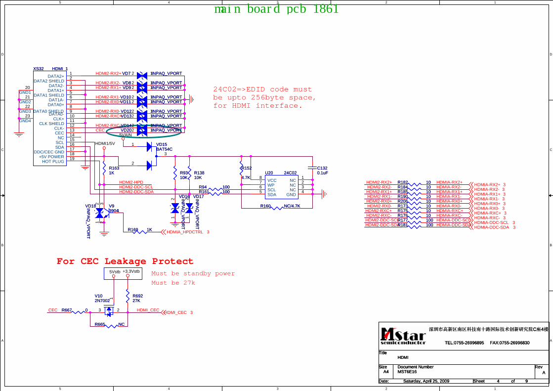
24C02=>EDID code mustbe upto 256byte space,for HDMI interface.
Must be 27k
For CEC Leakage ProtectMust be standby power
HDMI2-RX1+HDMI2-RX2-
HDMI2-RX1-HDMI2-RX0+
HDMI2-RX0-HDMI2-RXC+
HDMI2-RXC-
HDMI2-DDC-SDAHDMI2-DDC-SCL
HDMI2-RX2+
CEC
HDMI2-HPD
HDMIA-DDC-SCLHDMIA-DDC-SDA
HDMI2-DDC-SCLHDMI2-DDC-SDA
HDMI2-RX1+HDMI2-RX2-
HDMI2-RX1-HDMI2-RX0+HDMI2-RX0-
HDMI2-RXC+HDMI2-RXC-
HDMI2-RX2+
HDMIA-RX1+HDMIA-RX2-
HDMIA-RX1-HDMIA-RX0+HDMIA-RX0-HDMIA-RXC+HDMIA-RXC-
HDMIA-RX2+
HDMI_CECCEC
5VAIN
HDMI1/5V
+3.3Vstb5Vstb
HDMIA_HPDCTRL 3
HDMIA-RX2+ 3HDMIA-RX2- 3HDMIA-RX1+ 3HDMIA-RX1- 3
HDMIA-DDC-SDA 3HDMIA-DDC-SCL 3
HDMIA-RX0+ 3HDMIA-RX0- 3HDMIA-RXC+ 3HDMIA-RXC- 3
HDMI_CEC 3
Title
Size Document Number Rev
Date: Sheet of
深圳市高新区南区科技南十路国际技术创新研究院C座4楼
TEL:0755-26996895 FAX:0755-26996830
MST6E16 A
HDMI
A4
4 9Saturday, April 25, 2009
Title
Size Document Number Rev
Date: Sheet of
深圳市高新区南区科技南十路国际技术创新研究院C座4楼
TEL:0755-26996895 FAX:0755-26996830
MST6E16 A
HDMI
A4
4 9Saturday, April 25, 2009
Title
Size Document Number Rev
Date: Sheet of
深圳市高新区南区科技南十路国际技术创新研究院C座4楼
TEL:0755-26996895 FAX:0755-26996830
MST6E16 A
HDMI
A4
4 9Saturday, April 25, 2009
R1631KR1631K
R185 10R185 10
VD9 INPAQ_VPORTVD9 INPAQ_VPORT12
R175 10R175 10
R152
4.7K
R152
4.7K
C1320.1uFC1320.1uF
XS32 HDMI_1XS32 HDMI_1
DATA2+1
DATA2 SHIELD2
DATA2-3
DATA1+4
DATA1 SHIELD5
DAT1A-6
DATA0+78
DATA0 SHIELDDATA0-
9
CLK+10
CLK SHIELD11
CLK-12
CEC13
NC14
SCL15
SDA16
DDC/CEC GND17
+5V POWER18
HOT PLUG19
20GND1
21GND2
22GND3
23GND4
VD15BAT54CVD15BAT54C
3
1
2
R13810KR13810K
R667 0R667 0
VD12 INPAQ_VPORTVD12 INPAQ_VPORT12
R160 NC/4.7KR160 NC/4.7K R173 10R173 10R206 10R206 10
R181 100R181 100R169 1KR169 1K
VD14 INPAQ_VPORTVD14 INPAQ_VPORT12
R184 10R184 10
VD18INP
AQ
_V
PO
RT
VD18INP
AQ
_V
PO
RT
12
R190 10R190 10
R177 100R177 100
VD10 INPAQ_VPORTVD10 INPAQ_VPORT12
R161 100R161 100
VD11 INPAQ_VPORTVD11 INPAQ_VPORT12
U20 24C02U20 24C02
NC1
NC2
NC3
GND4
SDA5 SCL6 WP7 VCC8
R9310KR9310K
VD17INP
AQ
_V
PO
RT
VD17INP
AQ
_V
PO
RT
12
R94 100R94 100
V102N7002V102N7002
1
3 2
R665 NCR665 NC
VD16INP
AQ
_V
PO
RT
VD16INP
AQ
_V
PO
RT
12
VD20 INPAQ_VPORTVD20 INPAQ_VPORT12
R176 10R176 10
R182 10R182 10
V93904V939041
23
VD13 INPAQ_VPORTVD13 INPAQ_VPORT12
VD7 INPAQ_VPORTVD7 INPAQ_VPORT12
VD8 INPAQ_VPORTVD8 INPAQ_VPORT12
R69227KR69227K
main board pcb 1861
5
5
4
4
3
3
2
2
1
1
D D
C C
B B
A A
YPbPr
SCART1 RGB Input
VGA-SCL
VGA-Rin
VGA-SDA
VS_RGB
HS_RGB
TXD0
RXD0
VGA-Bin
VGA-Gin
VGA-HS
VGA-VS
VGA-SCLVGA-SDA
RIN+
GIN+SOG
BIN+
PC-Rin
PC-Lin
HD1_Yin
HD1_Prin
AU-SW0
HD1_Pbin
SC1_GinSC1_BinSC1_Rin
SC1_GSC1_B
SC1_R
SC1_Rin
SC1_Gin
SC1_Bin
SC1_R
SC1_B
SC1_G
HD1_Yin
HD1_Prin
SC1_Gin
SC1_Bin
SC1_Rin
HD1_Pbin
HD1_Yin
HD1_Pbin
HD1_Prin
HD1_YinHD1_PbinHD1_Prin
PC_R
PC_L
VGA/5V
5VAIN
VGA/5V VGA-DDC-5V
5VAIN
5VAIN
5VAIN
5VAIN 5VAIN
RXD0 3
TXD0 3
HS_RGB 3
VS_RGB 3
BIN+ 3
GIN+ 3
RIN+ 3SOG 3
SOY 3
PB+ 3PR+ 3
Y+ 3
PC-Lin 3
PC-Rin 3
SC1_G 6SC1_B 6
SC1_R 6
AU-SW03,6
Title
Size Document Number Rev
Date: Sheet of
深圳市高新区南区科技南十路国际技术创新研究院C座4楼
TEL:0755-26996895 FAX:0755-26996830
MST6E16 A
VGA&Component
A3
5 9Friday, July 24, 2009
Title
Size Document Number Rev
Date: Sheet of
深圳市高新区南区科技南十路国际技术创新研究院C座4楼
TEL:0755-26996895 FAX:0755-26996830
MST6E16 A
VGA&Component
A3
5 9Friday, July 24, 2009
Title
Size Document Number Rev
Date: Sheet of
深圳市高新区南区科技南十路国际技术创新研究院C座4楼
TEL:0755-26996895 FAX:0755-26996830
MST6E16 A
VGA&Component
A3
5 9Friday, July 24, 2009
C355 2.2uFC355 2.2uF
R32547KR32547K
R31547KR31547K
R111 100R111 100
VD59ESD
VD59ESD
12
C124560pFC124560pF
R97 47R97 47
R31375R31375
VD58ESD
VD58ESD
12
R96 47R96 47
R213 10KR213 10K
R32847KR32847K
R9975R9975
VD131BAV99VD131BAV99
3
2
1
VD62INP
AQ
_VP
OR
T
VD62INP
AQ
_VP
OR
T
12
R10175R10175
R210 10KR210 10K
C375 2.2uFC375 2.2uF
R56 47R56 47
R32447KR32447K
R32647KR32647KR50
75R5075
R116 NCR116 NC
VD64ESD
VD64ESD
12
VD129BAV99VD129BAV99
3
2
1
R33047KR33047K
VD116BAV99VD116BAV99
3
2
1
R343 1KR343 1K
R49 47R49 47
R114 100R114 100
R1104.7KR1104.7K
VD60ESDVD60ESD
12
R113 100R113 100
VD321
ESD
VD321
ESD
VD65ESDVD65ESD
12 C382 2.2uFC382 2.2uF
VD67BAT54CVD67BAT54C
3
1
2
C1450.1uFC1450.1uF
VD319
ESD
VD319
ESD
R5575R5575
R32347KR32347K
R115 100R115 100
R59 470R59 470
R106 100R106 100
XS36VGAXS36VGA
5104938271
15
14
13
12
116
16
17
R1124.7KR1124.7K
VD72ESDVD72ESD
12
R348 22R348 22
R98 470R98 470
VD71ESDVD71ESD
12
C354 2.2uFC354 2.2uF
VD70ESDVD70ESD
12
C112560pFC112560pF
R89 NC/0R89 NC/0
VD115BAV99VD115BAV99
3
2
1
R1072.2KR1072.2K
R1082.2KR1082.2K
U30 PI5V330/NCU30 PI5V330/NC
S1A2
S1B5
S1C11
S1D14
S2A3
S2B6
S2C10
S2D13
IN1
DA4
DB7
DC9
DD12
VCC16
GND8
EN15
R31475R31475
R31275R31275
U16 24C02U16 24C02
NC1
NC2
NC3
GND4
SDA5SCL6VCLK7VCC8
C1290.1uFC1290.1uF
C376 2.2uFC376 2.2uF
VD66ESDVD66ESD
12
R143 0/NCR143 0/NC
R32747KR32747K
R105 100R105 100
R16410KR16410K
R144 0/NCR144 0/NC
R34447KR34447K
R58 47R58 47
R32947KR32947K
VD318
ESD
VD318
ESDR1094.7KR1094.7K
R82 NC/0R82 NC/0
R145 0/NCR145 0/NC
R142 0/NCR142 0/NC
VD322
ESD
VD322
ESD
VD117BAV99VD117BAV99
3
2
1
R146 0/NCR146 0/NC
R95 47R95 47
R141 0/NCR141 0/NC
R5775R5775
C357 2.2uFC357 2.2uF
VD130BAV99VD130BAV99
3
2
1
R
L
Y
Pb
Pr
XS7
AV1
R
L
Y
Pb
Pr
XS7
AV1
1
3
5
66
8
1212
22
44
99
1313
1414
1515
77
1616
1010
1111
1717
1818
1919
2020
VD63ESDVD63ESD
12
VD320
ESD
VD320
ESD
R81 NC/0R81 NC/0
R75747KR75747K
R32247KR32247K
R10075R10075
R16210KR16210K
VD61INP
AQ
_VP
OR
T
VD61INP
AQ
_VP
OR
T
12
main board pcb 1861

5
5
4
4
3
3
2
2
1
1
D D
C C
B B
A A
S-Video Input
AV2 Input
LocationNear RCA.
AU-SW1 AU-SW0 Output0
1 110 1
0
0 AV1_L/RAV2_L/R
AV OutputSCART1 Input
Blanking I/O
Switch
AV1 Input
0: AV mode 1: TV mode
C193调至C194,解决Kp、Kr及黑电平相关
AV1-Rin
AV1-IN AV1-Vin+
AV1-Lin
Scart1_Lout
AV2-IN AV2-Vin+
AV1-L
AV1-R
SV1-C SV1-Cin
SV1-YinSV1-Y
AV2-Vin-
Scart1_R
Scart1_L
Scart1_Rout
AV1-Vin-
AU-SW1
AV2-Lin
AV2-Rin
MUX-Rin
MUX-Lin
AU-SW0
AV1-Lin
AV1-Rin
SV1-YSV1-C
AV2-IN
AV2-L
AV2-R
Scart1_Vout
Scart1_Lout
Scart1_Rout
SC1-L
Scart1_L
SC1-R
Scart1_R
AV2-L
AV2-Rin
AV2-Lin
AV2-R
AV1-IN
AV1-L
AV1-R
SC1_GSC1_B
SC1_R
Scart1_Rout
AV2-LSC1_B
AV2-INScart1_VOUT
AV2-R
SC1_RSC_FB
SC1_G
SC_FS
Scart1_Lout
GAIN_SW
GAIN_SW
CVBSOut
Scart1_VOUT
5VAIN_4052
5VAIN
+12V +12V
5VAIN
+12V
5VAIN_4052
AV1-Vin+ 3
SV1-Cin 3
SV1-Yin 3
AV2-Vin+ 3
AV2-Vin- 3
AV1-Vin- 3
AU-SW13AU-SW03,5
MUX-Lin 3
MUX-Rin 3
SC1-L 3 SC1-R 3
SC1_G 5SC1_B 5
SC_FS 3
SC_FB 3
SC1_R 5
GAIN_SW 3
GAIN_SW 3
CVBSOut 3
Title
Size Document Number Rev
Date: Sheet of
深圳市高新区南区科技南十路国际技术创新研究院C座4楼
TEL:0755-26996895 FAX:0755-26996830
MST6E16 A
Video input
A3
6 9Friday, July 24, 2009
Title
Size Document Number Rev
Date: Sheet of
深圳市高新区南区科技南十路国际技术创新研究院C座4楼
TEL:0755-26996895 FAX:0755-26996830
MST6E16 A
Video input
A3
6 9Friday, July 24, 2009
Title
Size Document Number Rev
Date: Sheet of
深圳市高新区南区科技南十路国际技术创新研究院C座4楼
TEL:0755-26996895 FAX:0755-26996830
MST6E16 A
Video input
A3
6 9Friday, July 24, 2009
C8170.1uFC8170.1uF
R20127KR20127K
R18812KR18812K
R675 47R675 47
C34410uFC34410uF
R19312KR19312K
R186 47R186 47
黄
白
红
左
中
右
下AV_INXS1B
黄
白
红
左
中
右
下AV_INXS1B
8
9
11
13
10
1214
R375 10KR375 10K
R669 47R669 47
VD90ESDVD90ESD
12
C328 2.2uFC328 2.2uF
R671 10kR671 10k
R228 47R228 47
C5201nFC5201nF
R6684.7KR6684.7K
R3
49
47
K/N
CR
34
94
7K
/NC
R3
46
47
K/N
CR
34
64
7K
/NC
R288NC/10KR288NC/10K
R408 100R408 100
C276 2.2uFC276 2.2uF
VD89ESDVD89ESD
12
R6744.7KR6744.7K
V143904V143904
1
23
R67847R67847
R18775R18775
R2
91
47
KR
29
14
7K
VD88ESDVD88ESD
12
VD95ESDVD95ESD
12
R28575R28575
V163904V163904
1
23
R3
10
47
KR
31
04
7K
V133904V133904
1
23
R23075R23075
C1920.1uFC1920.1uF
C3200.1uFC3200.1uF
R198220
R198220
R2
95
47
KR
29
54
7K
R281 27KR281 27K
C346
10
uF
C346
10
uF
VD93ESDVD93ESD
12
GND
YinCin
GNDGND
XS31 S-Video
GND
YinCin
GNDGND
XS31 S-Video3124567
R17912KR17912K
R211 47R211 47
C193NCC193NC
白
红
下左
右
XS2BSIDE_AV_IN/AV2
白
红
下左
右
XS2BSIDE_AV_IN/AV2
+CA8 100uF/16V+CA8 100uF/16VR311 0R311 0
VD86ESDVD86ESD
12
C218 2.2uFC218 2.2uF
VD85ESDVD85ESD
12
VD92ESDVD92ESD
12
U28 74HC4052U28 74HC4052
X012
X114
X215
X311
Y01
Y15
Y22
Y34
A10
B9
X13
Y3
VCC16
GND8
INH6
VEE7
C34810uFC34810uF
R289 0/10KR289 0/10K
R22575R22575
R196100KR196100K
C190560pFC190560pF
VD94ESDVD94ESD
12
R407 100R407 100
V123906V123906
1
32
R6798.2KR6798.2K
R19975R19975
C347
10
uF
C347
10
uF
R677 10kR677 10k
R268 4.7KR268 4.7K
R20510KR20510K
R195 47R195 47R67247R67247
R67047KR67047K
R374 10KR374 10K
R242 10KR242 10K
R67647KR67647K
R3
47
47
K/N
CR
34
74
7K
/NC
C194560pFC194560pF
C216 2.2uFC216 2.2uF
R3
20
47
K/N
CR
32
04
7K
/NC
VD84ESDVD84ESD
12
R287 8.2KR287 8.2K
黄
白
红
左
中
右
上AV_OUTXS1A
黄
白
红
左
中
右
上AV_OUTXS1A
1
2
4
6
3
57
C329 2.2uFC329 2.2uF
V153904V153904
1
23
XS39SCART1XS39SCART1
2
4
6
8
10
12
14
16
18
20
1
3
5
7
9
11
13
15
17
19
24
25
21
23
22
R6738.2KR6738.2K
C277 2.2uFC277 2.2uF
VD83ESDVD83ESD
12
C33910uFC33910uF
C5191nFC5191nF
R20410KR20410K
R194330R194330
黄
上左
XS2ASIDE_AV_IN/AV2
黄
上左
XS2ASIDE_AV_IN/AV2
R223 4.7KR223 4.7K
VD96ESDVD96ESD
12
R202150R202150
R200
220
R200
220
L18 FB/10KL18 FB/10K
R17412KR17412K
R2861.5KR2861.5K
R166 47R166 47
V19
3904
V19
39041
23
R222 47R222 47
C187560pFC187560pF
VD91ESDVD91ESD
12
R218 47R218 47
C324 2.2uFC324 2.2uF
C185560pFC185560pF
C184560pFC184560pF
R2
93
47
KR
29
34
7K
C325 2.2uFC325 2.2uF
R244 10KR244 10K
R373 10KR373 10K
R385 10KR385 10K
R16875R16875
main board pcb 1861
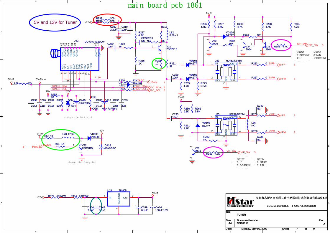
5
5
4
4
3
3
2
2
1
1
D D
C C
B B
A A
5V and 12V for Tuner
change the footprint
change the footprintN62740: NTSC1: PAL
N94550: M/N1: BG/DK/I
N94530: BG/DK/I/L1: L'
N62570: L'1: BG/DK/I/L
SIF_SW
I2C_SDAI2C_SCL
SIFM
SIFP
VIFM
VIFP
TUNER_SCLTUNER_SDA
TAGCIF_TV
PWM3
VIF_SW
5V-IF
33V40V
5V-IF
5V-IF
+12V
5V-Tuner
+12V
+12V40V
5V-IF
TAGC 3
I2C_SDA 3I2C_SCL 3
SIF_SW 3
SIFP 3
SIFM 3
VIFP 3
VIFM 3
PWM33
VIF_SW 3
Title
Size Document Number Rev
Date: Sheet of
深圳市高新区南区科技南十路国际技术创新研究院C座4楼
TEL:0755-26996895 FAX:0755-26996830
MST6E16 A
TUNER
A4
7 9Tuesday, May 05, 2009
Title
Size Document Number Rev
Date: Sheet of
深圳市高新区南区科技南十路国际技术创新研究院C座4楼
TEL:0755-26996895 FAX:0755-26996830
MST6E16 A
TUNER
A4
7 9Tuesday, May 05, 2009
Title
Size Document Number Rev
Date: Sheet of
深圳市高新区南区科技南十路国际技术创新研究院C座4楼
TEL:0755-26996895 FAX:0755-26996830
MST6E16 A
TUNER
A4
7 9Tuesday, May 05, 2009
C2490.1uFC2490.1uF
R362
100K
R362
100K
R263NCR263NC
R233 300R233 300
D66
UP574
D66
UP574
R241
NC/75
R241
NC/75
CA14100uF/16VCA14100uF/16V
R259 0R259 0
R250 12KR250 12K
CA13
NC/47uF/16V
CA13
NC/47uF/16V R2626.8KR2626.8K
R2584.7KR2584.7K
L820.82uHL820.82uH
C23510nFC23510nF
C2480.1uFC2480.1uF
R319NCR319NC
R2554.7KR2554.7K
R353 4.7KR353 4.7K
C230
22pF
C230
22pF
R2364.7KR2364.7K
R3314.7KR3314.7K
R376 10R/2WR376 10R/2W
R29810R29810
R260 0R260 0
C21910nFC21910nF
R38210KR38210K
R2974.7KR2974.7K
R2612.2KR2612.2K
R51 1KR51 1K
R251 47R251 47
C222NCC222NC
R2384.7KR2384.7K
R273NC/0R273NC/0
R2541KR2541K
R284 NCR284 NC
C242NCC242NC
C233
22pF
C233
22pF
V253904V253904
1
23
C238
0.1uF
C238
0.1uF
C236NCC236NC
V222SC1815V222SC1815
1
23
R2566.8KR2566.8K
C234
0.1uF
C234
0.1uF
R253 0R253 0
C226
0.1uF
C226
0.1uF
+ CA1810uF/50V
+ CA1810uF/50V
VD106BA277VD106BA277
R53 10R53 10
VD107 1N4148VD107 1N4148
U22 TDQ-6F6/T126CWU22 TDQ-6F6/T126CW
AG
C1
NC
12
AS
3
SC
L4
SD
A5
5V
A6
5V
B7
NC
38
33
V9
NC
41
0
IFo
ut
11
GN
D3
12
GN
D2
13
GN
D1
14
GN
D4
15
GN
D5
16
GN
D6
17
GN
D7
18
GN
D8
19
R317
680
R317
680
R257 0R257 0
U24 78M05U24 78M05
IN1
OUT2
TA
B/G
ND
3
V233904V2339041
23
C22910nFC22910nF
R31856R31856
R32139R32139
V212SC2216V212SC2216
1
2
3
SAWU23 N9453/N9455
SAWU23 N9453/N9455
2ING
4OUT1G
ND
3
5OUT21 IN
R2374.7KR2374.7K
R234 300R234 300
VD104BA277VD104BA277
R3161KR3161K
C22010nFC22010nF
R352 4.7KR352 4.7K
V243904V243904
1
23
VD108BA277VD108BA277
R252 47R252 47
C299
2.2uF
C299
2.2uF
R384 10R/2WR384 10R/2W
+ CA1910uF/50V
+ CA1910uF/50V
L66NCL66NC
L81 FBL81 FB
L20 470uHL20 470uH
C3042.2uFC3042.2uF
VD105BA277VD105BA277
VD1091N4148VD1091N4148
V203904V2039041
23
SAWU25 N6257/N6274
SAWU25 N6257/N6274
2ING
4OUT1G
ND
3
5OUT21 IN
C3002.2uFC3002.2uF
main board pcb 1861

5
5
4
4
3
3
2
2
1
1
D D
C C
B B
A A
TPA1517(可兼容TDA1517P,10、11NC即可)
AMP-L
OP_VCC1
OP_VCC1
AMP-RPH-Rin
PH-Lin
PH-Lout
PH-Rout
PH-Lout PH-Lin
PH-RinPH-Rout
HP_MUTE_AMP
AMP-LOUT
AMP-L
AMP-R
PH-Lin
PH-Rin
PWD_MT
AMP-ROUT
HP_MUTE_AMP
+12V
6VBuf1
5VAIN +12V
+12V
+12V +12V_IN+12V +12V+12V_IN+12V_IN
AMP-L3
AMP-R3
AMP-R3
AMP-L3
AMP-MUTE3
Title
Size Document Number Rev
Date: Sheet of
深圳市高新区南区科技南十路国际技术创新研究院C座4楼
TEL:0755-26996895 FAX:0755-26996830
MST6E16 A
Amplifier
A3
8 9Monday, April 27, 2009
Title
Size Document Number Rev
Date: Sheet of
深圳市高新区南区科技南十路国际技术创新研究院C座4楼
TEL:0755-26996895 FAX:0755-26996830
MST6E16 A
Amplifier
A3
8 9Monday, April 27, 2009
Title
Size Document Number Rev
Date: Sheet of
深圳市高新区南区科技南十路国际技术创新研究院C座4楼
TEL:0755-26996895 FAX:0755-26996830
MST6E16 A
Amplifier
A3
8 9Monday, April 27, 2009
L31 FBL31 FB
V7033904V7033904
1
23
C480 225C480 225
+ CA24100uF/16V
+ CA24100uF/16V
-
+
U45ATL062
-
+
U45ATL0623
21
84
R282 470R282 470
VD114NC/1N4148VD114NC/1N4148
Q2Q2
+CA29
470uF/16V
+CA29
470uF/16VR455 33KR455 33K
R2802.2KR2802.2K
R3874.7KR3874.7K
R338
NC
R338
NC
C340 2.2uFC340 2.2uF
M2
CONN RECT 1
M2
CONN RECT 1
1
H5
NC/HOLE-V8
H5
NC/HOLE-V8
1
2
3
4
5
6
7
8
CA93 100uF/16VCA93 100uF/16V
+CA28 470uF/16V+CA28 470uF/16V
R2272.2MR2272.2M
-
+
U45BTL062
-
+
U45BTL0625
67
84
R332
0R
R332
0R
VD1111N4148VD1111N4148
R43910KR43910K
R2
77
22
KR
27
72
2K
H2
NC/HOLE-V8
H2
NC/HOLE-V8
1
2
3
4
5
6
7
8
R267 10KR267 10KC343 2.2uFC343 2.2uF
R459 33KR459 33K
R40347KR40347K
+CA2122uF
+CA2122uF
R302470R302470
C3421nFC3421nF
C183 2.2uFC183 2.2uF
R275 NCR275 NC
H4
NC/HOLE-V8
H4
NC/HOLE-V8
1
2
3
4
5
6
7
8
TPA1517U26 TPA1517U26
IN11
SGND2
SVRR3
OUT14
PGND5
OUT26
VCC7
M_SB8
IN29
GND12GND13GND14GND15GND16GND17GND18GND19GND20
GND10
GND11
Q5Q5
VD19BAV99VD19BAV99
3
2
1
VD1121N4148VD1121N4148
C1
88
1n
FC
18
81
nF
H6
NC/HOLE-V8
H6
NC/HOLE-V8
1
2
3
4
5
6
7
8
R278 2.2KR278 2.2K
R337
0R
R337
0R
R239 1KR239 1K
XS41HeadPhoneXS41HeadPhone
R3
WR4
WL2
L1
AGND5
R40247KR40247K
R437100R437100
C1791nFC1791nF
Q9Q9
H1
NC/HOLE-V8
H1
NC/HOLE-V8
1
2
3
4
5
6
7
8
R34510RR34510R
R41210KR41210K
R3340RR3340R
XP25ShieldXP25Shield
123456
M3
CONN RECT 1
M3
CONN RECT 1
1
V7023904V7023904
1
23
R2658k2R2658k2
XP28XP28
1234
C3410.1uFC3410.1uF
R301470R301470
+
CA22220uF/25V+
CA22220uF/25V
C1600.1uFC1600.1uF
+CA26 470uF/16V+CA26 470uF/16V
R41533KR41533K
V273904V273904
1
23
R24022KR24022K
R44110KR44110K
H3
NC/HOLE-V8
H3
NC/HOLE-V8
1
2
3
4
5
6
7
8
R41610KR41610K
C1
91
1n
FC
19
11
nF
M1
CONN RECT 1
M1
CONN RECT 1
1
R226 10R226 10
VD1101N4148VD1101N4148
C478 100pFC478 100pF
+CA83100uF/16V
+CA83100uF/16V
R2
76
22
KR
27
62
2K
R246 1KR246 1K
CA92 100uF/16VCA92 100uF/16V
C189 2.2uFC189 2.2uF
R333
NC
R333
NC
V7013906V7013906
C479 100pFC479 100pF
R2792.2KR2792.2K
C11NCC11NC
R335NCR335NC
R274 NCR274 NC
+CA84 100uF/16V+CA84 100uF/16V
Q3Q3
R283 470R283 470
D703 NC/BA240D703 NC/BA240
R2242.2MR2242.2M
R360100KR360100K
+CA20
470uF/25V
+CA20
470uF/25V
R414 33KR414 33K
R336
100K
R336
100K
R247 NC/0R247 NC/0
VD701BAV99VD701BAV99
3
12
main board pcb 1861

5
5
4
4
3
3
2
2
1
1
D D
C C
B B
A A
Version A:在LCD22W57DEU_ZB_1701_C的基础上更改。
Page11、STANDBY部分待机低功耗IC电路,注意采用原芯片增加R37、R38 0R;2、BL_ON/OFF、BL_ADJUST上拉电压预留;3、USB滤波电容位置预留;Page21、DCDC部分待机低功耗IC电路,L8物料更换(成本),注意采用原芯片增加L16、更换L8;2、VDDP、VDDP_PM调整,注意涉及电容排布,建议丝印依照原理图;Page31、LED、PWMB、HDMI_CEC等网络调整,注意采用原芯片增加R683;2、ON_USB1、ON_PANEL上拉增加;3、PW_CTL调整,注意IC差异;4、部分GPIO上拉电压更改,参照紫红标注部分;Page61、4052 VCC电路优化,兼容原板增加R289 0R;2、CVBSout VCC滤波电容,增加C346、C347;Page4-6压敏电阻封装更改为0402,注意兼容原板定额更改;Page7增加R352、R353,注意兼容原板定额更改。
Version B:在MST6E16JS_ZB_1861_A的基础上更改。
Page11、CA6位置调整,避免部分屏掉电残影等问题;Page21、删除L19、L21;//改板方便,不再更改;Page31、删除R456、R480;//改板方便,不再更改;2、调整LED网络,删除R684,增加R427;3、PCB增加主芯片散热焊盘;Page61、增加C194;
Title
Size Document Number Rev
Date: Sheet of
深圳市高新区南区科技南十路国际技术创新研究院C座4楼
TEL:0755-26996895 FAX:0755-26996830
MST6E16 A
Revision
A4
9 9Thursday, July 30, 2009
Title
Size Document Number Rev
Date: Sheet of
深圳市高新区南区科技南十路国际技术创新研究院C座4楼
TEL:0755-26996895 FAX:0755-26996830
MST6E16 A
Revision
A4
9 9Thursday, July 30, 2009
Title
Size Document Number Rev
Date: Sheet of
深圳市高新区南区科技南十路国际技术创新研究院C座4楼
TEL:0755-26996895 FAX:0755-26996830
MST6E16 A
Revision
A4
9 9Thursday, July 30, 2009
main board pcb 1861


