John H. Lau, Stephen H. Pan, and Chris ChangExpress Packaging Systems, Inc.1705 Junction CourtSan Jose, Calfornia 95112Phone: 408-435-4836Fax: 408-435-6983e-mail: [email protected]
Abstract
An empirical equation for predicting the thermal-fatigue life of wafer level chip scale package (WLCSP) solder joints on PrintedCircuit Board (PCB) is presented in this work. The solder joints are subjected to thermal cycling and their crack lengths at differentthermal cycles are measured. Also, the J-integrals at the crack tip of different crack lengths in the corner solder joint are determinedby nonlinear fracture mechanics with Finite Element method.
One of the unique feature of most WLCSPs is the use of ametal layer to redistribute the very fine-pitch peripheral-arrayedpads on the chip to much larger-pitch area-arrayed pads withmuch taller solder joints on the PCB 1-5. In general, with WLCSPs,the underfill encapsulant may not be necessary. However, due tothe very large thermal expansion mismatch between the siliconchip and the FR-4 epoxy PCB, WLCSP’s solder joint reliabilityis one of the critical issues in the applications of WLCSPs onPCB without underfill encapsulant.
In Reference 4, an empirical equation for predicting the ther-mal-fatigue life of WLCSP solder joints has been presented. How-
ever, it was based on linear fracture mechanics and the resultingequation was in terms of the stress intensity factors at the cracktip of the solder joint. In this work, the solder is assumed to be anelastic-plastic material with temperature dependent, and the re-sulting equation is in terms of the J-integrals at the crack tip ofthe solder joint.
In the present approach, the crack length of a WLCSP solderjoint is measured as a function of the number of thermal cycles.By combining the nonlinear fracture characteristics such as theJ-integrals at the crack tip of different crack lengths, an empiri-cal equation for predicting the thermal-fatigue life of WLCSPsolder joints is proposed.
2. WLCSP Assembly
2.1. The Wafer
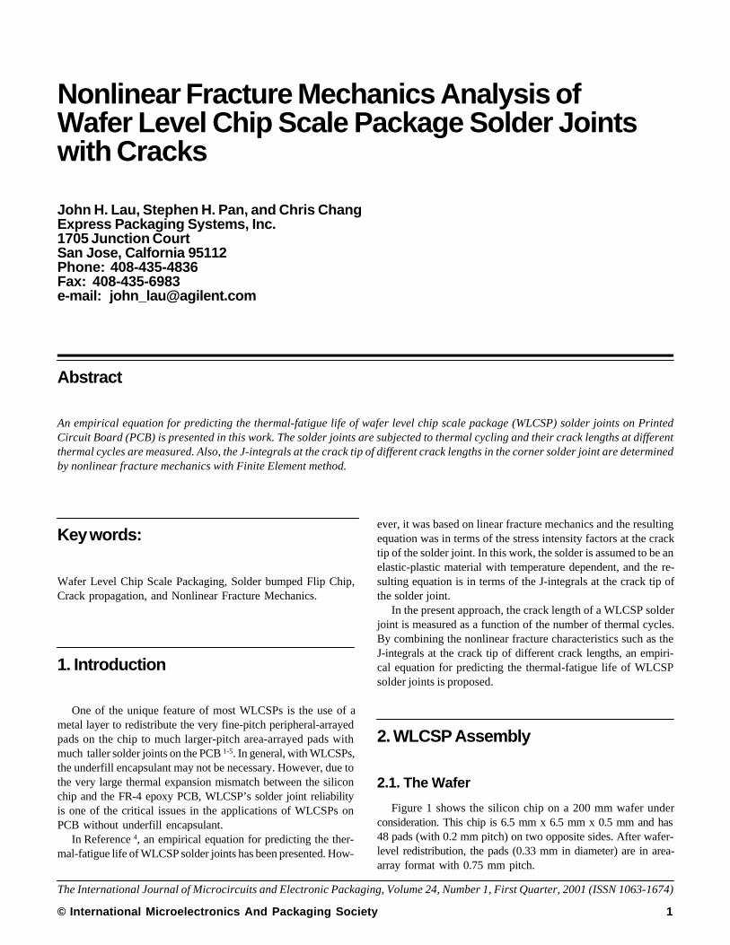
Figure 1 shows the silicon chip on a 200 mm wafer underconsideration. This chip is 6.5 mm x 6.5 mm x 0.5 mm and has48 pads (with 0.2 mm pitch) on two opposite sides. After wafer-level redistribution, the pads (0.33 mm in diameter) are in area-array format with 0.75 mm pitch.
The International Journal of Microcircuits and Electronic Packaging, Volume 24, Number 1, First Quarter, 2001 (ISSN 1063-1674)
Intl. Journal of Microcircuits and Electronic Packaging
2
1
2
3
4
5
6
7
8
9
10
11
12
13
14
15
16
17
18
19
20
21
22
23
24
25
26
27
28
29
30
31
32
33
34
35
36
37
38
39
40 48
47
46
45
44
43
42
41
Figure 1. A memory chip with redistribution pads.
2.2. The WLCSP
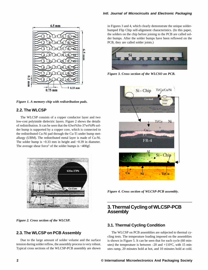
The WLCSP consists of a copper conductor layer and twolow-cost polyimide dielectric layers. Figure 2 shows the detailsof redistribution. It can be seen that the 63wt%Sn-37wt%Pb sol-der bump is supported by a copper core, which is connected tothe redistributed Cu-Ni pad through the Cu-Ti under bump met-allurgy (UBM). The redistributed metal layer is made of Cu-Ni.The solder bump is ~0.33 mm in height and ~0.39 in diameter.The average shear force5 of the solder bumps is ~400gf.
Figure 2. Cross section of the WLCSP.
2.3. The WLCSP on PCB Assembly
Due to the large amount of solder volume and the surfacetension during solder reflow, the assembly process is very robust.Typical cross sections of the WLCSP-PCB assembly are shown
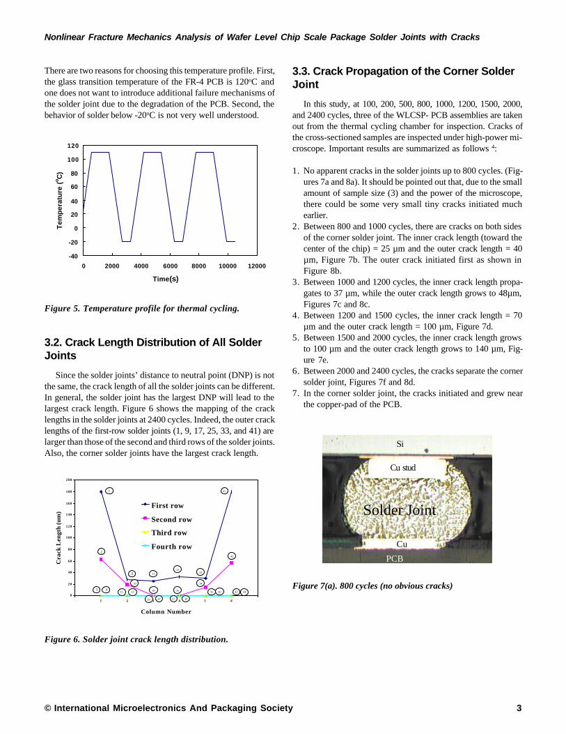
in Figures 3 and 4, which clearly demonstrate the unique solder-bumped Flip Chip self-alignment characteristics. (In this paper,the solders on the chip before joining to the PCB are called sol-der bumps. After the solder bumps have been reflowed on thePCB, they are called solder joints.)
Figure 3. Cross section of the WLCSO on PCB.
Al
Cu PI
Si - Chip
Ni Ti/Cu
Si - Chip
Ti/Cu Ni Cu
Solder Joint
Si - Chip Ti/Cu/Cu/Ni
Cu stud
FR-4 Cu
Figure 4. Cross section of WLCSP-PCB assembly.
3. Thermal Cycling of WLCSP-PCBAssembly
3.1. Thermal Cycling Condition
The WLCSP on PCB assemblies are subjected to thermal cy-cling tests. The temperature loading imposed on the assembliesis shown in Figure 5. It can be seen that for each cycle (60 min-utes) the temperature is between –20 and +110oC, with 15 min-utes ramp, 20 minutes hold at hot, and 10 minutes hold at cold.
63Sn-37Pb
Si
Nonlinear Fracture Mechanics Analysis of Wafer Level Chip Scale Package Solder Joints with Cracks
The International Journal of Microcircuits and Electronic Packaging, Volume 24, Number 1, First Quarter, 2001 (ISSN 1063-1674)
There are two reasons for choosing this temperature profile. First,the glass transition temperature of the FR-4 PCB is 120oC andone does not want to introduce additional failure mechanisms ofthe solder joint due to the degradation of the PCB. Second, thebehavior of solder below -20oC is not very well understood.
-40
-20
0
20
40
60
80
100
120
0 2000 4000 6000 8000 10000 12000
Time (sec)
Tem
per
atu
re (
o C)
Figure 5. Temperature profile for thermal cycling.
3.2. Crack Length Distribution of All SolderJoints
Since the solder joints’ distance to neutral point (DNP) is notthe same, the crack length of all the solder joints can be different.In general, the solder joint has the largest DNP will lead to thelargest crack length. Figure 6 shows the mapping of the cracklengths in the solder joints at 2400 cycles. Indeed, the outer cracklengths of the first-row solder joints (1, 9, 17, 25, 33, and 41) arelarger than those of the second and third rows of the solder joints.Also, the corner solder joints have the largest crack length.
0
20
40
60
80
100
120
140
160
180
200
0 1 2 3 4 5 6 7
Column Number
Cra
ck L
engt
h (u
m)
First row
Second row
Third row
Fourth row
1
9
2
312
4
17
25
41
33
42
18
10
26
34
11 35 36 43 44
282719 20
Figure 6. Solder joint crack length distribution.
3.3. Crack Propagation of the Corner SolderJoint
In this study, at 100, 200, 500, 800, 1000, 1200, 1500, 2000,and 2400 cycles, three of the WLCSP- PCB assemblies are takenout from the thermal cycling chamber for inspection. Cracks ofthe cross-sectioned samples are inspected under high-power mi-croscope. Important results are summarized as follows 4:
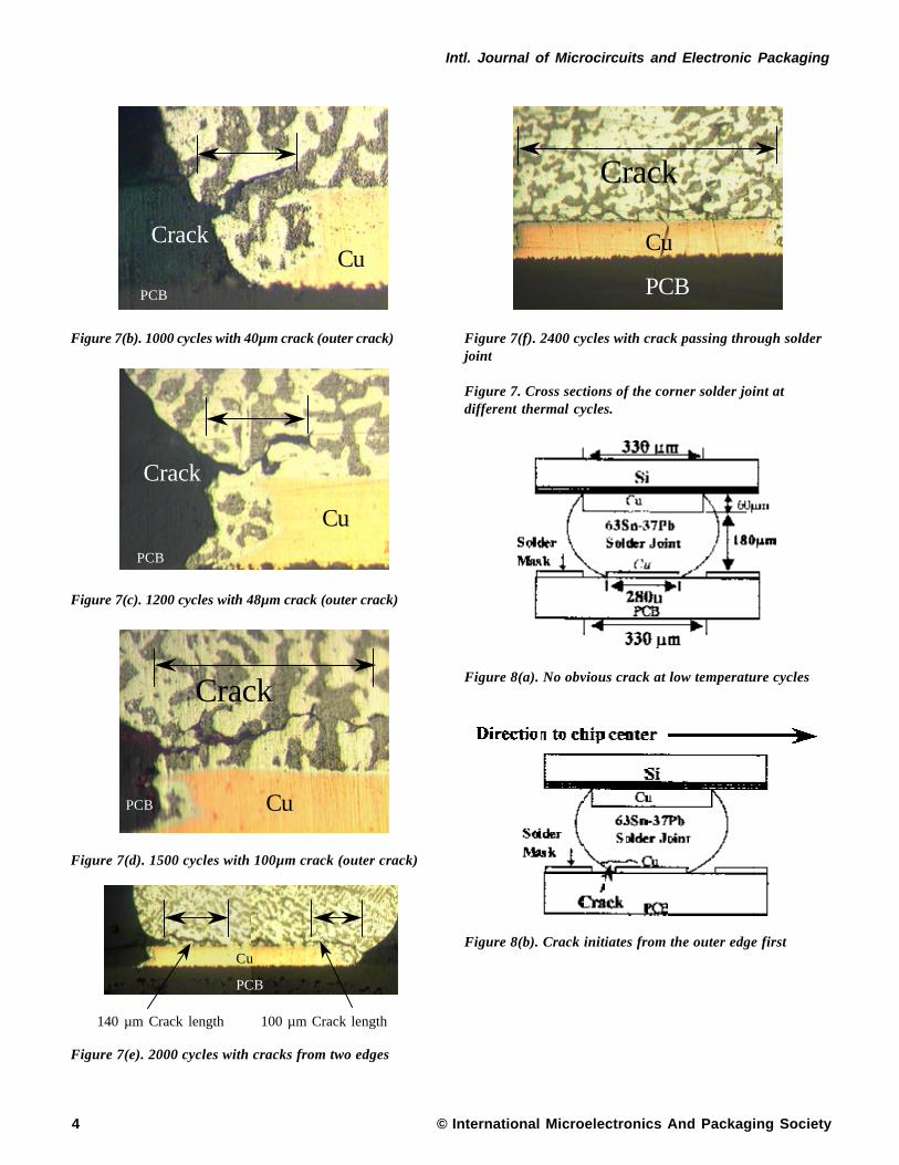
1. No apparent cracks in the solder joints up to 800 cycles. (Fig-ures 7a and 8a). It should be pointed out that, due to the smallamount of sample size (3) and the power of the microscope,there could be some very small tiny cracks initiated muchearlier.
2. Between 800 and 1000 cycles, there are cracks on both sidesof the corner solder joint. The inner crack length (toward thecenter of the chip) = 25 µm and the outer crack length = 40µm, Figure 7b. The outer crack initiated first as shown inFigure 8b.
3. Between 1000 and 1200 cycles, the inner crack length propa-gates to 37 µm, while the outer crack length grows to 48µm,Figures 7c and 8c.
4. Between 1200 and 1500 cycles, the inner crack length = 70µm and the outer crack length = 100 µm, Figure 7d.
5. Between 1500 and 2000 cycles, the inner crack length growsto 100 µm and the outer crack length grows to 140 µm, Fig-ure 7e.
6. Between 2000 and 2400 cycles, the cracks separate the cornersolder joint, Figures 7f and 8d.
7. In the corner solder joint, the cracks initiated and grew nearthe copper-pad of the PCB.
Figure 8(c). Crack initiates from the inner edge later
Figure 8(d). Cracks grow through the whole solder joint
Figure 8. Schematic of the corner solder joint at differentstages of thermal cycles.
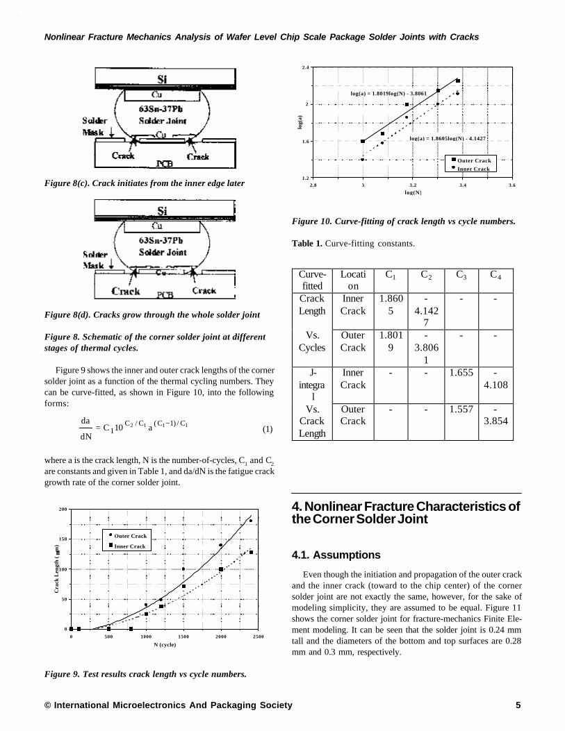
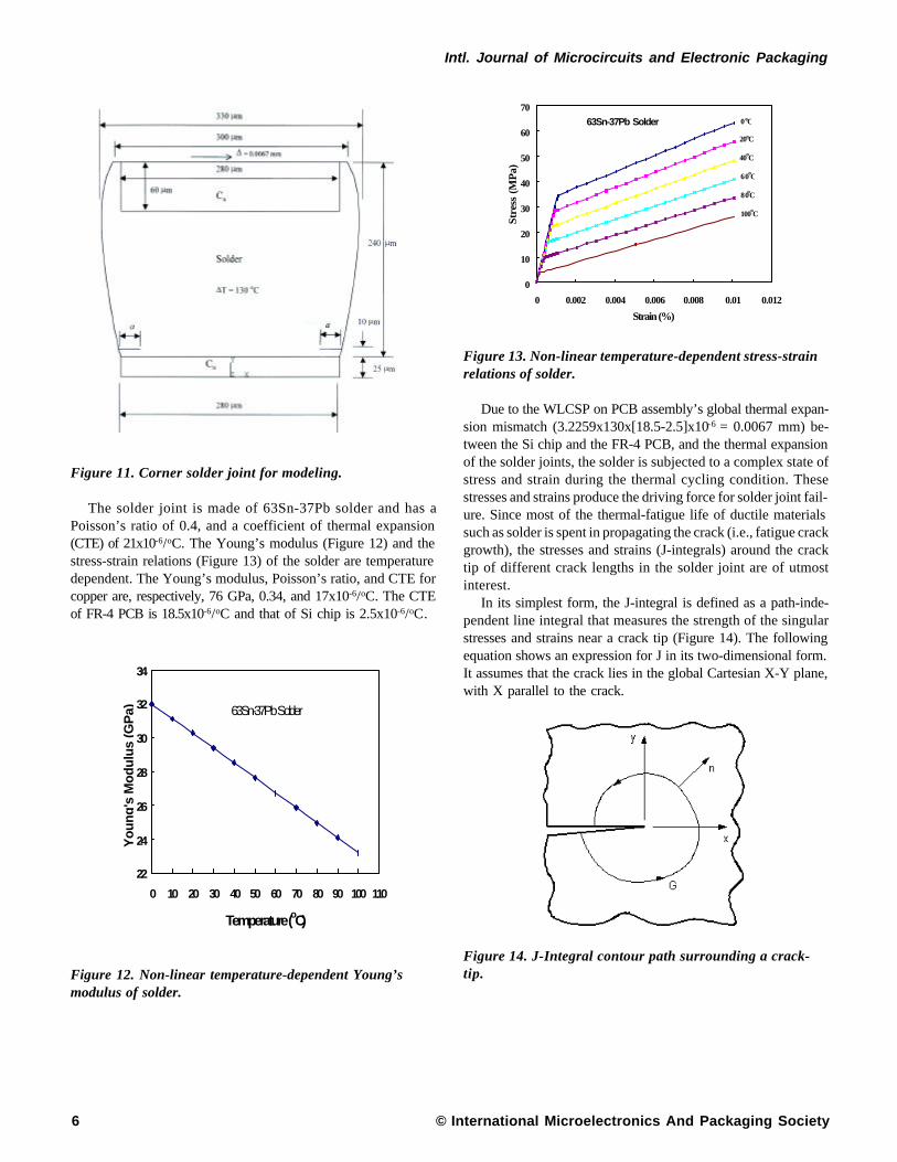
Figure 9 shows the inner and outer crack lengths of the cornersolder joint as a function of the thermal cycling numbers. Theycan be curve-fitted, as shown in Figure 10, into the followingforms:
1112 C/)1C(C/C1 a10C
dN
da −= (1)
where a is the crack length, N is the number-of-cycles, C1 and C2
are constants and given in Table 1, and da/dN is the fatigue crackgrowth rate of the corner solder joint.
0
50
100
150
200
0 500 1000 1500 2000 2500
N (cycle)
Cra
ck L
engt
h (
µµm)
Outer Crack
Inner Crack
Figure 9. Test results crack length vs cycle numbers.
log(a) = 1.8605log(N) - 4.1427
log(a) = 1.8019log(N) - 3.8061
1.2
1.6
2
2.4
2.8 3 3.2 3.4 3.6
log(N)
log(
a)
Outer Crack
Inner Crack
Figure 10. Curve-fitting of crack length vs cycle numbers.
Even though the initiation and propagation of the outer crackand the inner crack (toward to the chip center) of the cornersolder joint are not exactly the same, however, for the sake ofmodeling simplicity, they are assumed to be equal. Figure 11shows the corner solder joint for fracture-mechanics Finite Ele-ment modeling. It can be seen that the solder joint is 0.24 mmtall and the diameters of the bottom and top surfaces are 0.28mm and 0.3 mm, respectively.
The International Journal of Microcircuits and Electronic Packaging, Volume 24, Number 1, First Quarter, 2001 (ISSN 1063-1674)
Intl. Journal of Microcircuits and Electronic Packaging
6
Figure 11. Corner solder joint for modeling.
The solder joint is made of 63Sn-37Pb solder and has aPoisson’s ratio of 0.4, and a coefficient of thermal expansion(CTE) of 21x10-6/oC. The Young’s modulus (Figure 12) and thestress-strain relations (Figure 13) of the solder are temperaturedependent. The Young’s modulus, Poisson’s ratio, and CTE forcopper are, respectively, 76 GPa, 0.34, and 17x10-6/oC. The CTEof FR-4 PCB is 18.5x10⁻⁶/oC and that of Si chip is 2.5x10⁻⁶/oC.
22
24
26
28
30
32
34
0 10 20 30 40 50 60 70 80 90 100 110
Temperature (oC)
You
ng's
Mod
ulus
(GP
a) 63Sn-37Pb Solder
Figure 12. Non-linear temperature-dependent Young’smodulus of solder.
0
10
20
30
40
50
60
70
0 0.002 0.004 0.006 0.008 0.01 0.012
Strain (%)
Stre
ss (
MP
a)
0oC
20oC
40oC
60oC
80oC
100oC
63Sn-37Pb Solder
Figure 13. Non-linear temperature-dependent stress-strainrelations of solder.
Due to the WLCSP on PCB assembly’s global thermal expan-sion mismatch (3.2259x130x[18.5-2.5]x10-6 = 0.0067 mm) be-tween the Si chip and the FR-4 PCB, and the thermal expansionof the solder joints, the solder is subjected to a complex state ofstress and strain during the thermal cycling condition. Thesestresses and strains produce the driving force for solder joint fail-ure. Since most of the thermal-fatigue life of ductile materialssuch as solder is spent in propagating the crack (i.e., fatigue crackgrowth), the stresses and strains (J-integrals) around the cracktip of different crack lengths in the solder joint are of utmostinterest.
In its simplest form, the J-integral is defined as a path-inde-pendent line integral that measures the strength of the singularstresses and strains near a crack tip (Figure 14). The followingequation shows an expression for J in its two-dimensional form.It assumes that the crack lies in the global Cartesian X-Y plane,with X parallel to the crack.
Figure 14. J-Integral contour path surrounding a crack-tip.
Nonlinear Fracture Mechanics Analysis of Wafer Level Chip Scale Package Solder Joints with Cracks
The International Journal of Microcircuits and Electronic Packaging, Volume 24, Number 1, First Quarter, 2001 (ISSN 1063-1674)
where:G = any path surrounding the crack tip,W = strain energy density,tx = traction along x axis = sxnx +sxy ny,
ty = traction along y axis = syny + sxy nx,
s = stress component,n = unit outward normal to path,u = displacement, ands = distance along the path.
In this study, five different crack lengths are considered. Thesecracks are located symmetrically 10 mm above the copper pad onthe PCB. The 8-node plain strain element is used in this studyand the units are in Newton and mm. At the crack tip, the mid-side nodes are placed at the quarter points to capture the singu-larity in the stresses.
4.2. Boundary Conditions
The boundary conditions imposed on the corner solder jointare shown in Figure 11, where the bottom surface is fixed, thetop surface (nodes) of the solder joint is subjected to a 0.0067mm displacement, and the whole solder joint is subjected to atemperature change of 130oC. The top surface is also restrainedfrom rotation by specifying nodal couplings of vertical displace-ment to those nodes in order for the vertical displacements to bethe same.
With the prescribed loadings, the left crack in Figure 11 isexpected to pop open and the right crack should remain close.Instead of using contact elements, nodal couplings are conve-niently used to simulate the closing and sliding of the right cracksurfaces. In ANSYS (a commercial Finite Element code) 6, thenodes on the right crack surfaces are nodal-coupled in the verti-cal direction at the coincident nodes, while free to slide in thehorizontal direction. Using nodal couplings, there is no penetra-tion of the crack surfaces when the crack is closed.
Figures 15 through 19 show the deformed (with Finite Ele-ment meshes) and un-deformed shapes of the corner solder jointwith different crack lengths: 0.056, 0.084, 0.112, 0.1225, and0.133 mm. The typical von Mises stress contours around the cracktips (with a crack length = 0.112 mm) are shown in Figure 20. Itcan be seen that, due to stress concentration, the stresses at thecrack tip are very large. The J-integrals at the inner and outercrack tips for different crack lengths of the corner solder joint areshown in Figure 21.
Figure 15. Deformed shape of the corner solder joint (cracklength = 0.056 mm, DDJ_inner crack = 0.0704 MPa-mm,DDJ_outer crack = 0.0791 MPa-mm).
Figure 16. Deformed shape of the corner solder joint(crack length = 0.084 mm, DDJ_inner crack = 0.0918 MPa-mm, DDJ_outer crack = 0.126 MPa-mm).
Figure 17. Deformed shape of the corner solder joint(crack length = 0.112 mm, DDJ_inner crack = 0.175 MPa-mm, DDJ_outer crack = 0.183 MPa-mm).
Figure 21. J-Integral range of different crack length in thecorner solder joint.
5. Thermal-Fatigue Life PredictionModel
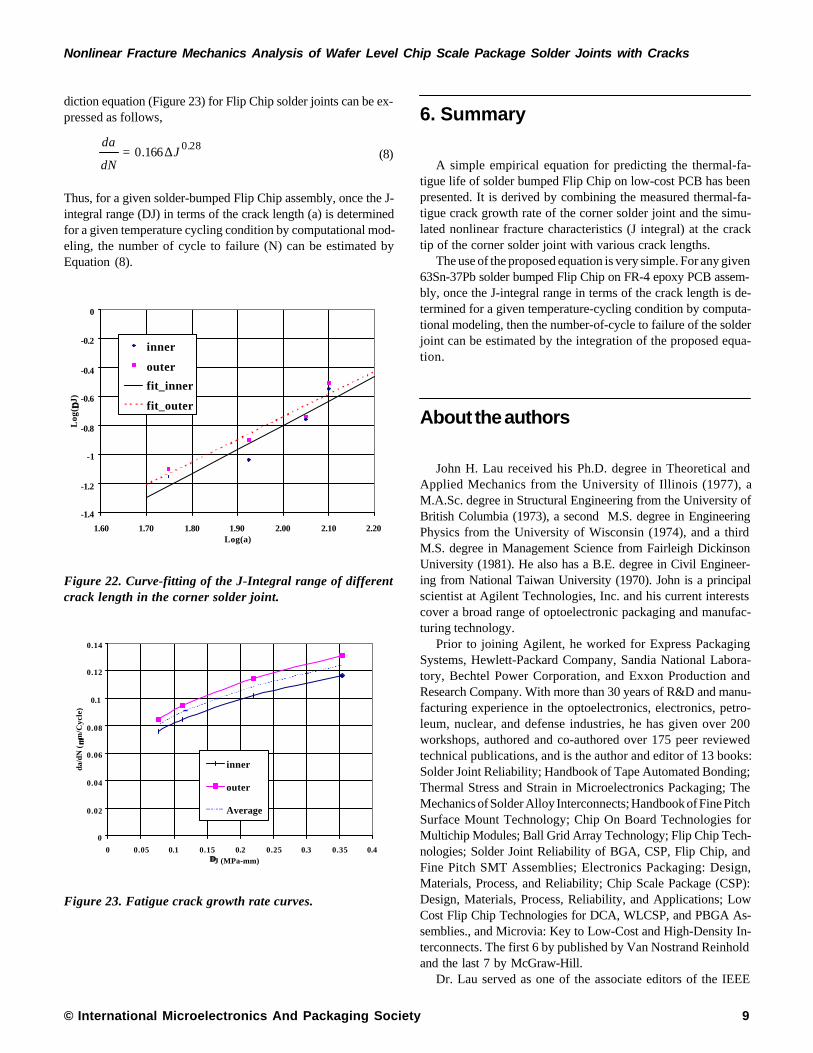
The curves in Figure 21 can be curve-fitted, as shown in Fig-ure 22 [only four points are used since the solder joint fracture(near the fifth point) is not stable], into the following forms:
43 )log()log( CaCJ +=∆ (3)
or
334/1/10
CCCJa ∆−= (4)
The constants C3 and C4 are given in Table 1. Substituting Equa-tion (4) into Equation (1) yields,
3113144132/)1(/)(
110CCCCCCCCCC
JCdN
da −+−∆= (5)
Thus, for the inner crack, C1 = 1.8606; C2 = -4.1427; C3 = 1.655;C4 = -4.108, and Equation (5) becomes,
279.0155.0 J
dN
da∆= (6)
For the outer crack, C1 = 1.8019; C2 = -3.8061; C3 = 1.557; C4 =-3.854, and Equation (5) becomes,
286.0176.0 J
dN
da∆= (7)
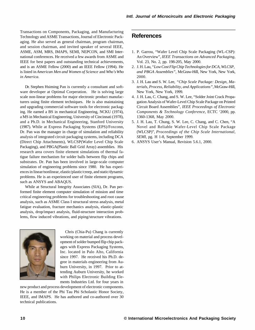
Equations (6) and (7) are shown in Figure 23. By averaging thecoefficients of Equations (6) and (7), the thermal-fatigue life pre-
Nonlinear Fracture Mechanics Analysis of Wafer Level Chip Scale Package Solder Joints with Cracks
The International Journal of Microcircuits and Electronic Packaging, Volume 24, Number 1, First Quarter, 2001 (ISSN 1063-1674)
diction equation (Figure 23) for Flip Chip solder joints can be ex-pressed as follows,
28.0166.0 J
dN
da∆= (8)
Thus, for a given solder-bumped Flip Chip assembly, once the J-integral range (DJ) in terms of the crack length (a) is determinedfor a given temperature cycling condition by computational mod-eling, the number of cycle to failure (N) can be estimated byEquation (8).
-1.4
-1.2
-1
-0.8
-0.6
-0.4
-0.2
0
1.60 1.70 1.80 1.90 2.00 2.10 2.20Log(a)
Log
( ∆∆J)
inner
outer
fit_inner
fit_outer
Figure 22. Curve-fitting of the J-Integral range of differentcrack length in the corner solder joint.
0
0.02
0.04
0.06
0.08
0.1
0.12
0.14
0 0.05 0.1 0.15 0.2 0.25 0.3 0.35 0.4∆∆J (MPa-mm)
da/d
N (
µµm/C
ycle
)
inner
outer
Average
Figure 23. Fatigue crack growth rate curves.
6. Summary
A simple empirical equation for predicting the thermal-fa-tigue life of solder bumped Flip Chip on low-cost PCB has beenpresented. It is derived by combining the measured thermal-fa-tigue crack growth rate of the corner solder joint and the simu-lated nonlinear fracture characteristics (J integral) at the cracktip of the corner solder joint with various crack lengths.
The use of the proposed equation is very simple. For any given63Sn-37Pb solder bumped Flip Chip on FR-4 epoxy PCB assem-bly, once the J-integral range in terms of the crack length is de-termined for a given temperature-cycling condition by computa-tional modeling, then the number-of-cycle to failure of the solderjoint can be estimated by the integration of the proposed equa-tion.
About the authors
John H. Lau received his Ph.D. degree in Theoretical andApplied Mechanics from the University of Illinois (1977), aM.A.Sc. degree in Structural Engineering from the University ofBritish Columbia (1973), a second M.S. degree in EngineeringPhysics from the University of Wisconsin (1974), and a thirdM.S. degree in Management Science from Fairleigh DickinsonUniversity (1981). He also has a B.E. degree in Civil Engineer-ing from National Taiwan University (1970). John is a principalscientist at Agilent Technologies, Inc. and his current interestscover a broad range of optoelectronic packaging and manufac-turing technology.
Prior to joining Agilent, he worked for Express PackagingSystems, Hewlett-Packard Company, Sandia National Labora-tory, Bechtel Power Corporation, and Exxon Production andResearch Company. With more than 30 years of R&D and manu-facturing experience in the optoelectronics, electronics, petro-leum, nuclear, and defense industries, he has given over 200workshops, authored and co-authored over 175 peer reviewedtechnical publications, and is the author and editor of 13 books:Solder Joint Reliability; Handbook of Tape Automated Bonding;Thermal Stress and Strain in Microelectronics Packaging; TheMechanics of Solder Alloy Interconnects; Handbook of Fine PitchSurface Mount Technology; Chip On Board Technologies forMultichip Modules; Ball Grid Array Technology; Flip Chip Tech-nologies; Solder Joint Reliability of BGA, CSP, Flip Chip, andFine Pitch SMT Assemblies; Electronics Packaging: Design,Materials, Process, and Reliability; Chip Scale Package (CSP):Design, Materials, Process, Reliability, and Applications; LowCost Flip Chip Technologies for DCA, WLCSP, and PBGA As-semblies., and Microvia: Key to Low-Cost and High-Density In-terconnects. The first 6 by published by Van Nostrand Reinholdand the last 7 by McGraw-Hill.
Dr. Lau served as one of the associate editors of the IEEE
The International Journal of Microcircuits and Electronic Packaging, Volume 24, Number 1, First Quarter, 2001 (ISSN 1063-1674)
Intl. Journal of Microcircuits and Electronic Packaging
10
References
1. P. Garrou, “Wafer Level Chip Scale Packaging (WL-CSP):An Overview”, IEEE Transactions on Advanced Packaging,Vol. 23, No. 2, pp. 198-205, May 2000.
2. J. H. Lau, “Low Cost Flip Chip Technologies for DCA, WLCSP,and PBGA Assemblies”, McGraw-Hill, New York, New York,2000.
3. J. H. Lau and S. W. Lee, “Chip Scale Package: Design, Ma-terials, Process, Reliability, and Applications”, McGraw-Hill,New York, New York, 1999.
4. J. H. Lau, C. Chang, and S. W. Lee, “Solder Joint Crack Propa-gation Analysis of Wafer-Level Chip Scale Package on PrintedCircuit Board Assemblies”, IEEE Proceedings of ElectronicComponents & Technology Conference, ECTC ‘2000, pp.1360-1368, May 2000.
5. J. H. Lau, T. Chung, S. W. Lee, C. Chang, and C. Chen, “ANovel and Reliable Wafer-Level Chip Scale Package(WLCSP)”, Proceedings of the Chip Scale International,SEMI, pg. H 1-8, September 1999.
6. ANSYS User’s Manual, Revision 5.6.1, 2000.
Transactions on Components, Packaging, and ManufacturingTechnology and ASME Transactions, Journal of Electronic Pack-aging. He also served as general chairman, program chairman,and session chairman, and invited speaker of several IEEE,ASME, ASM, MRS, IMAPS, SEMI, NEPCON, and SMI Inter-national conferences. He received a few awards from ASME andIEEE for best papers and outstanding technical achievements,and is an ASME Fellow (2000) and an IEEE Fellow (1994). Heis listed in American Men and Women of Science and Who’s Whoin America.
Dr. Stephen Hsiming Pan is currently a consultant and soft-ware developer at Optimal Corperation. He is solving largescale non-linear problems for major electronic product manufac-turers using finite element techniques. He is also maintainingand upgrading commercial software tools for electronic packag-ing. He earned a BS in mechanical Engineering, NCKU (1974),a MS in Mechanical Engineering, University of Cincinnati (1978),and a Ph.D. in Mechanical Engineering, Stanford University(1987). While at Express Packaging Systems (EPS)/Foxconn,Dr. Pan was the manager in charge of simulation and reliabilityanalysis of integrated circuit packaging systems, including DCA(Direct Chip Attachments), WLCSP(Wafer Level Chip ScalePackaging), and PBGA(Plastic Ball Grid Array) assemblies. Hisresearch area covers finite element simulations of thermal fa-tigue failure mechanism for solder balls between flip chips andsubstrates. Dr. Pan has been involved in large-scale computersimulation of engineering problems since 1980. He has experi-ences in linear/nonlinear, elastic/plastic/creep, and static/dynamicproblems. He is an experienced user of finite element programs,such as ANSYS and ABAQUS.
While at Structural Integrity Associates (SIA), Dr. Pan per-formed finite element computer simulation of mission and timecritical engineering problems for troubleshooting and root causeanalysis, such as ASME Class I structural stress analysis, metalfatigue evaluation, fracture mechanics analysis, elastic-plasticanalysis, drop/impact analysis, fluid-structure interaction prob-lems, flow induced vibrations, and piping/structure vibrations.
Chris (Chia-Pu) Chang is currentlyworking on material and process devel-opment of solder bumped flip chip pack-ages with Express Packaging Systems,Inc. located in Palo Alto, Californiasince 1997. He received his Ph.D. de-gree in materials engineering from Au-burn University, in 1997. Prior to at-tending Auburn University, he workedwith Philips Electronic Building Ele-ments Industries Ltd. for four years in
new product and process development of electronic components.He is a member of the Phi Tau Phi Scholastic Honor Society,IEEE, and IMAPS. He has authored and co-authored over 30technical publications.