Novel piezoelectric actuation mechanism for a gimbal-less mirror in 2D raster scanning applications This article has been downloaded from IOPscience. Please scroll down to see the full text article. 2011 J. Micromech. Microeng. 21 075001 (http://iopscience.iop.org/0960-1317/21/7/075001) Download details: IP Address: 122.126.116.119 The article was downloaded on 02/06/2011 at 03:33 Please note that terms and conditions apply. View the table of contents for this issue, or go to the journal homepage for more Home Search Collections Journals About Contact us My IOPscience
Transcript
Novel piezoelectric actuation mechanism for a gimbal-less mirror in 2D raster scanning
applications
This article has been downloaded from IOPscience. Please scroll down to see the full text article.
2011 J. Micromech. Microeng. 21 075001
(http://iopscience.iop.org/0960-1317/21/7/075001)
Download details:
IP Address: 122.126.116.119
The article was downloaded on 02/06/2011 at 03:33
Please note that terms and conditions apply.
View the table of contents for this issue, or go to the journal homepage for more
Home Search Collections Journals About Contact us My IOPscience
IOP PUBLISHING JOURNAL OF MICROMECHANICS AND MICROENGINEERING
J. Micromech. Microeng. 21 (2011) 075001 (9pp) doi:10.1088/0960-1317/21/7/075001
Novel piezoelectric actuation mechanismfor a gimbal-less mirror in 2D rasterscanning applicationsKah How Koh1, Takeshi Kobayashi2, Jin Xie3, Aibin Yu4 andChengkuo Lee1,5
1 Department of Electrical & Computer Engineering, National University of Singapore, 4 EngineeringDrive 3, Singapore 1175762 National Institute of Advanced Industrial Science and Technology (AIST), 1-2-1 Namiki, Tsukuba,Ibaraki 305-8564, Japan3 Institute of Microelectronics (IME), Agency for Science, Technology and Research (A∗STAR),11 Science Park Road, Singapore 1176854 Micron Semiconductor Asia Pte Ltd, 990 Bendemeer Road, Singapore 339942
Received 22 August 2010, in final form 14 April 2011Published 1 June 2011Online at stacks.iop.org/JMM/21/075001
AbstractIn this paper, we present the design, fabrication and measurement results of a 2D scanningmirror actuated by 1 × 10 piezoelectric Pb(Zr,Ti)O3 (PZT) cantilever actuators integrated on athin silicon beam. A combination of bulk silicon micromachining based on asilicon-on-insulator (SOI) substrate and thin-film surface micromachining on a 5 μm thick Sidevice layer is used to fabricate the device. Multi-layers of Pt/Ti/PZT/Pt/Ti are deposited aselectrode materials. A large silicon mirror plate (5 mm × 5 mm) and a 1 × 10 PZT cantileverarray arranged in parallel are formed after the backside release process. The ten PZTcantilever actuators are electrically isolated from one another. The device can operate in threemodes: bending, torsional and mixed (or combinational) modes. In bending mode, the firstresonant frequency was measured to be 30 Hz and an optical deflection angle of ±8◦ wasobtained when all ten cantilevers were actuated at 9 Vpp. In torsional mode, the resonantfrequency was measured to be 89 Hz and an optical deflection angle of ±4.6◦ was obtained byapplying a gradually declining ac voltage started at 8 Vpp to two sets of actuators, where eachset comprises five cantilever actuators of the said 1 × 10 array, i.e. 1–5 and 6–10. A 2D rasterscanning pattern was achieved in the mixed mode when the bending mode was carried out bycantilever actuators of 4–7 and the torsional modes were exercised by two different sets ofcantilever actuators, i.e. 1–3 and 8–10, under opposite biasing direction. This mixed modeoperation mechanism demonstrates the first 2D raster scanning mirror-driven beam actuators.
(Some figures in this article are in colour only in the electronic version)
1. Introduction
Micro-opto-electro-mechanical systems (MOEMS) have beenpromising candidates in a wide variety of applications.These include various modules deployed in fiber opticcommunication networks such as tunable lasers [1],
5 Author to whom any correspondence should be addressed.
optical switches [2–5], variable optical attenuators [6–10],reconfigurable add/drop multiplexers [11]. In addition,MOEMS devices have also been conceptualized for a largerange of image display applications such as projection displays[12–14], biomedical imaging [15, 16] and retinal scanning[17, 18]. In recent years, micro-electro-mechanical systems(MEMS) display have formed a circle of growing interest,with the development of handheld pico-projectors based on
J. Micromech. Microeng. 21 (2011) 075001 K H Koh et al
scanning mirror technology becoming an intriguing killerapplication in consumer electronics, game consoles andautomobiles [13, 19]. The most well known commercialproduct is probably the digital micromirror device (DMD),which is the core of digital light processing (DLP) projectiontechnology developed by Texas Instrument in 1987 [20].In 1994, Solgaard et al developed the grating light valve(GLV) technology, providing an alternative technology forimplementation in commercial projectors [21].
Several research groups have successfully demonstratedscanning micromirrors using various actuation mechanisms,including electrostatic [22–27], electromagnetic [28–31],electrothermal [32–35] and piezoelectric [36–38] approaches.To achieve large mechanical rotation angles, gimbaled mirrorsusing torsion springs are the popular design for integrationwith the various actuation mechanisms. A gimbaled two-dimensional (2D) mirror [22–29, 35–38] normally consistsof two independent rotational axes placed orthogonally toeach other, allowing mechanical decoupling of the rotationof two axes and elimination of crosstalk of both drive signals.However, such a gimbaled design often requires a large portionof the die area to accommodate such structures, e.g. inner andouter frames needed for 2D scanning. In contrast, gimbal-less 2D mirrors [30, 32–34] realize two-axis scanning whileoffering advantages of single mirror and smaller footprintfor the same mirror size. The tradeoff, however, lies inthe dependence of the deflection of the mirror plate on themechanical action of all the actuators and the biasing schemeused to drive the actuators.
By having a mirror at the free end of a cantilever, Isikmanet al demonstrated 2D scanning patterns by using two sets ofac signals to oscillate this mirror which is coated with a NiFesoft magnetic film at a fundamental mode frequency (bendingmode) and second mode frequency (torsional mode) [30]. Jiaet al also reported a gimbal-less electrothermal tip-tilt-pistonmirror based on folded dual S-shaped bimorphs [32]. In thisdesign, the dual S-shaped bimorph actuators are connected tothe mirror plate by pure SiO2 joints, and this unique designallows for no lateral shift and rotation-axis shift for piston androtation scanning respectively. In another similar design by Xuet al, a circular single-crystal silicon mirror plate actuated bya folded curved thermal bimorph actuator was fabricated [33].The mirror plate was connected to the bimorphs by flexuralsprings, making the device capable of 3-DOF actuation. Amore straightforward and compact design was demonstratedby Schweizer et al [34]. In this work, the two orthogonalangular motions were given by the same ‘L’-shaped thermalbimorph cantilever beam, allowing 2D scanning to be madepossible by the simultaneous thermomechanical excitation ofthe cantilever.
A gimbal-less mirror for 2D scanning has also beenrealized by piezoelectric bending mode and torsional mode.This is illustrated in our previous reported research attempt,where a silicon micromirror driven by 1 × 10 piezoelectricPb(Zr,Ti)O3 beam actuators was fabricated and characterized[39]. In our previous work, we designed ten PZT actuatorsto be electrically connected in series and 2D Lissajousscan patterns are obtained by one-half of the actuators at a
resonant frequency corresponding to bending mode while theremaining other half of the actuators at a resonant frequencycorresponding to torsional mode. As such, the mirror in ourprevious work achieved torsional scanning solely by resonancephenomenon.
In this paper, a novel piezoelectric-driven scanningmirror using a mechanical supporting beam integrated with a1 × 10 PZT cantilever array is explored and characterized.This design is similar to that in [39], except that the electricalconnections to each of the cantilevers are now separated, henceallowing the cantilevers’ actuation behavior to be individuallymanipulated. More importantly, with the separated electricalconnections, we can now achieve torsional scanning basedon the difference in the ac biasing voltage applied to the tenpiezoelectric cantilevers. This actuation mechanism differsgreatly from that in [39] and the actuation mechanisms ofgimbaled mirror in torsional mode, i.e. the mirror rotationis generated against the torsion spring or torsion bar. Assuch, besides depending on the resonance phenomenon fortorsional scanning, the difference in the direction of cantileverdisplacement due to the 180◦ phase difference in the appliedbias also helps to magnify the torsional scanning of themirror. Although thermal bimorph beam actuators have beenwell characterized in terms of their capability of generatinglarge deflection, i.e. in bending mode, no design of torsionalmirror driven by beam actuators has been reported in thermalactuation and piezoelectric actuation schemes yet. As such,our unique design of piezoelectric cantilever beam actuator isthe first demonstration of a large torsion mirror using a beamactuator.
2. Design, modeling and fabrication
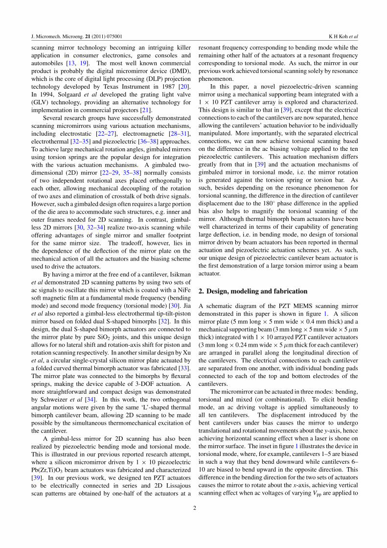
A schematic diagram of the PZT MEMS scanning mirrordemonstrated in this paper is shown in figure 1. A siliconmirror plate (5 mm long × 5 mm wide × 0.4 mm thick) and amechanical supporting beam (3 mm long × 5 mm wide × 5 μmthick) integrated with 1 × 10 arrayed PZT cantilever actuators(3 mm long × 0.24 mm wide × 5 μm thick for each cantilever)are arranged in parallel along the longitudinal direction ofthe cantilevers. The electrical connections to each cantileverare separated from one another, with individual bonding padsconnected to each of the top and bottom electrodes of thecantilevers.
The micromirror can be actuated in three modes: bending,torsional and mixed (or combinational). To elicit bendingmode, an ac driving voltage is applied simultaneously toall ten cantilevers. The displacement introduced by thebent cantilevers under bias causes the mirror to undergotranslational and rotational movements about the y-axis, henceachieving horizontal scanning effect when a laser is shone onthe mirror surface. The inset in figure 1 illustrates the device intorsional mode, where, for example, cantilevers 1–5 are biasedin such a way that they bend downward while cantilevers 6–10 are biased to bend upward in the opposite direction. Thisdifference in the bending direction for the two sets of actuatorscauses the mirror to rotate about the x-axis, achieving verticalscanning effect when ac voltages of varying Vpp are applied to
2
J. Micromech. Microeng. 21 (2011) 075001 K H Koh et al
Figure 1. Schematic diagram of a PZT 2D scanning mirror where it twists or bends when different ac voltage combinations are appliedseparately to the ten cantilevers. The inset shows torsional mode where a set of five cantilevers 1–5 bend in one direction, while the other setof five cantilevers 6–10 bend in the opposite direction.
the ten cantilevers. To obtain a 2D scan with two orthogonalscan axes, i.e. mixed mode, the ten cantilevers are biased suchthat both bending and torsional modes occur simultaneously,causing the mirror plate to rotate about the x- and y-axes at thesame time. The details of the biasing configuration to elicit a2D scan will be described in the later part of the paper.
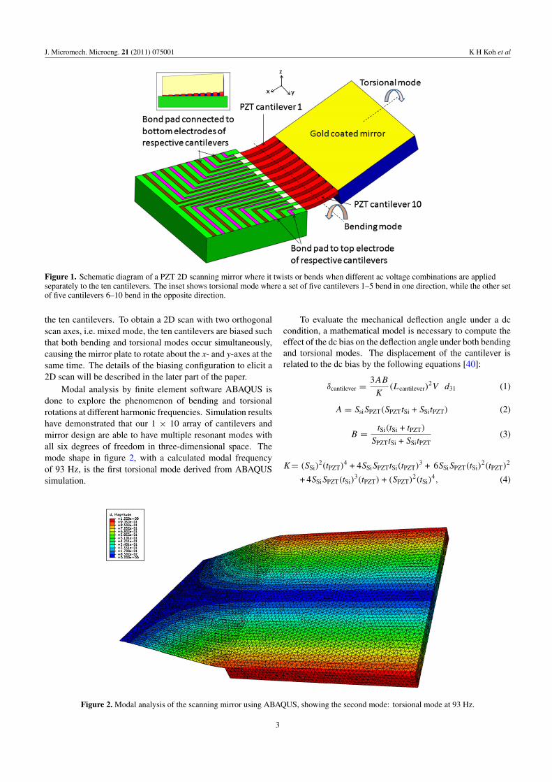
Modal analysis by finite element software ABAQUS isdone to explore the phenomenon of bending and torsionalrotations at different harmonic frequencies. Simulation resultshave demonstrated that our 1 × 10 array of cantilevers andmirror design are able to have multiple resonant modes withall six degrees of freedom in three-dimensional space. Themode shape in figure 2, with a calculated modal frequencyof 93 Hz, is the first torsional mode derived from ABAQUSsimulation.
Figure 2. Modal analysis of the scanning mirror using ABAQUS, showing the second mode: torsional mode at 93 Hz.
To evaluate the mechanical deflection angle under a dccondition, a mathematical model is necessary to compute theeffect of the dc bias on the deflection angle under both bendingand torsional modes. The displacement of the cantilever isrelated to the dc bias by the following equations [40]:
J. Micromech. Microeng. 21 (2011) 075001 K H Koh et al
(a)
(b)
Figure 3. Schematic drawing of the biased PZT cantilever with amirror plate during (a) bending mode, with a vertical displacementof δcantilever and mechanical rotation angle of θB ; (b) torsional mode,with a vertical displacement of δcantilever and mechanical rotationangle of θT .
where δ is the displacement of the actuator, Lcantilever is thelength of the cantilever (3 mm), V is the applied voltage,Ssi and SPZT are the compliances of the structural Si layer(6.0 × 10⁻¹² Pa−1) and PZT thin film (1.43 × 10⁻¹¹ Pa−1)respectively, tSi and tPZT are the respective thicknesses of thestructural silicon (5 μm) and PZT film (3 μm). The transversepiezoelectric constant, d31, may be assumed to be −100 pmV−1 when calculating the theoretical actuated displacementcaused by the piezoelectric effect.
Figure 3(a) relates the displacement of the cantilever tothe mechanical deflection angle of the mirror during bendingmode. Equation (5) can be derived from figure 3(a):
δcantilever = r − r cos θB, (5)
where δcantilever is the vertical displacement of the cantilevertip, r is the radius of curvature, θB is the mechanicaldeflection angle experienced by the cantilever under biasduring bending mode. Assuming that θB is small, by smallangle approximation,
cos θB = 1 − 12θ2
B (6)
r = Lcantilever
θB
. (7)
(a)
(b)
Figure 4. (a) Schematic diagram illustrating the cross section of thedevice after the microfabrication of PZT cantilever actuators andmirror. (b) A magnified photo showing the packaged device with agold-coated mirror surface. The bond pads are connected to thepackage via gold bond wires.
Substituting equations (1), (6) and (7) into (5) and making θB
the subject,
θB = 6ABLcantileverV d31
K. (8)
On the other hand, figure 3(b) is used to derive therelationship between the displacements of the cantilever andthe mechanical deflection angle of the mirror during torsionalmode:
sin θT = δcantilever
0.5Lmirror, (9)
where δcantilever is the vertical displacement of the cantilevertip, Lmirror is the length of the mirror, θT is the mechanicaldeflection angle experienced by the cantilever under biasduring torsional mode. Substituting equations (1) into (9)and making θT the subject,
θT = sin−1
(6ABL2
cantileverV d31
KLmirror
). (10)
Hence, from this mathematical analysis, the derivedequations (8) and (10) can be used to understand how a changein the dc bias affects the mechanical rotation angle duringbending and torsional modes respectively.
Figure 4(a) shows the schematic cross-sectionaldrawing of the PZT cantilever actuators and mirror aftermicrofabrication. The device is micromachined from a silicon-on-insulator (SOI) substrate of a 5 μm thick Si device layer,
4
J. Micromech. Microeng. 21 (2011) 075001 K H Koh et al
Figure 5. Frequency response measured for bending mode when asinusoidal ac voltage of 5 Vpp was applied to all ten PZT cantileverssimultaneously.
with multi-layers of Ti/Pt/LaNiO3/PZT/LaNiO3/Ti/Ptdeposited as electrode materials. The details of the fabricationprocess for this device can be obtained from [40, 41]. Tocompensate for the possible increase in dynamic deformationdue to a large scanning angle and frequency, a thick Sisubstrate is left beneath the mirror surface to maintain themirror flatness and rigidity. A thin film of gold was sputteredon the mirror surface using a shadow mask. This is to improvethe reflectivity of the mirror surface.
After the fabrication process, the device is assembled on adual in-line package (DIP) and the bond pads were connectedby gold bond wires to the metal pins of the DIP as shown infigure 4(b). To enhance the piezoelectric characteristics of thedevice, poling treatment is conducted on the PZT thin filmactuators at room temperature. A dc voltage of 30 V, whichis equivalent to a polarization electric field of 100 kV cm−1,was applied to each of the PZT thin film actuators for 5 min,with the poling direction from the bottom electrode to the topelectrode.
3. Results and discussion
3.1. Bending mode
In the bending mode operation of the PZT scanning mirror,the sinusoidal ac driving voltage was applied simultaneouslyto all the top electrodes of the cantilevers, while the bottomelectrodes of all the cantilevers were grounded. An He/Nelaser of wavelength 632.8 nm was shone on the mirror surface,forming a horizontal scan line trajectory on the screen. Opticaldeflection angles at different frequencies of the ac signalwere calculated using the horizontal scanned beam length andthe distance between the mircromirror and the screen. Thefrequency response for bending mode is shown in figure 5.An optical deflection angle (ODA) of ±3.8◦ was obtainedat 30 Hz when 5 Vpp was applied to all ten PZT cantilevers
Figure 6. Measured ODA versus peak-to-peak ac driving voltageapplied to all ten PZT cantilevers simultaneously during theresonance condition at 30 Hz.
simultaneously. This resonance frequency corresponds closelyto the first modal frequency of 31 Hz simulated by ABAQUS.Figure 6 shows the measured ODA for various Vpp appliedto the ten cantilevers during the resonance condition at30 Hz. The ODA increases rather linearly with increasingac driving voltage, reaching saturation for voltages above8 Vpp. An ODA of ±8◦ was obtained when an ac voltageof 10 Vpp was applied. The saturation behavior at an ODAof ±8◦ is due to the mirror plate coming into contact with thebottom of the package during the scanning operation, causingthe mirror oscillation at resonance to be damped and limited.The distance between the mirror plate and the base of the DIPhas been determined to be 500 μm using an optical microscope.
3.2. Torsional mode
Figure 7(a) illustrates the biasing configuration for torsionalmode operation. A potential divider was implemented to splitthe function generator ac output into five equal potentialsat the potential nodes between each resistor. The potentialdivider was realized by using five equal resistors of resistance20 � each connected in series. For the set of cantilevers1–5, the top electrodes for these cantilevers were connectedto the various potential nodes, while the bottom electrodesof these cantilevers were grounded. The reverse setup wasmade for the set of cantilevers 6–10, i.e. the top electrodes forthese cantilevers were grounded while the bottom electrodeswere connected to the various potential nodes. As a result,each cantilever will have a different ac bias amplitude asevident from the look-up table in figure 7(b). The results showthe largest and the smallest cantilever displacements whichare introduced at the mirror edges and center respectively.More importantly, the generated displacements for the twosets of cantilevers are toward opposite directions, resulting intorsional deflection of the mirror plate.
5
J. Micromech. Microeng. 21 (2011) 075001 K H Koh et al
(a) (b)
Figure 7. (a) Schematic drawing illustrating the electrical connections of the top and bottom electrodes of each cantilever to the functiongenerator for torsional mode operation. (b) A look-up table illustrating the individual Vpp bias driving each cantilever for the bias setupshown in (a).
Figure 8. Frequency response measured for torsional mode when asinusoidal ac voltage of 5 Vpp is applied by the function generator.
The frequency response for torsional mode is shown infigure 8. An ODA of ±4◦ was obtained when an ac voltageof 5 Vpp at 89 Hz was applied by the function generator.This resonant frequency obtained for the experimentally testeddevice corresponds closely to the simulated modal frequencyof 93 Hz obtained by ABAQUS.
Figure 9 shows the measured ODA for various Vpp appliedby the function generator during the resonance condition at89 Hz. An ODA of ±4.5◦ was obtained when an ac voltage of10 Vpp was applied. The observed saturation behavior above7 Vpp may suggest that the ODA of ±4.5◦ is the largest thatcan be achieved by the device in torsional mode operation,i.e. the torsional mechanical supporting beam has reached itsactuation limitation. In addition, for the same Vpp, a largerODA is obtained during bending mode, compared to torsionalmode. This is because of the larger torsional stiffness ofthe cantilever beam actuators as compared to their bendingstiffness. Moreover, the Vpp from the function generator was
Figure 9. Measured ODA versus peak-to-peak ac driving voltageapplied by the function generator during torsional mode.
simultaneously directly applied to all ten cantilever actuatorsin bending mode, while in torsional mode, the Vpp of thefunction generator was applied only to cantilevers 1 and 10,and the rest of the cantilever actuators 2–5 and 9–6 werebiased at a Vpp value gradually reduced and lower than that ofthe generator.
3.3. Mixed mode
In mixed (or combinational) mode operation, bending andtorsional actuations occur simultaneously to produce a 2DLissajous scanning pattern. Two functional generators wereused separately to bias cantilevers 4–7 at bending mode andcantilevers 1–3 and 8–10 at torsional mode, respectively. Asshown in figure 10(a), the sinusoidal ac driving voltage of30 Hz from the first function generator, V1,pp, was appliedsimultaneously to all the top electrodes of the cantilevers 4–7,while the bottom electrodes of the cantilevers were grounded.
6
J. Micromech. Microeng. 21 (2011) 075001 K H Koh et al
(a) (b)
Figure 10. (a) Schematic drawing illustrating the electrical connections of the top and bottom electrodes of each cantilever to the twofunction generators for mixed mode operation. (b) A look-up table illustrating the individual Vpp bias driving each cantilever for the biassetup shown in (a).
Figure 11. Measured ODA versus peak-to-peak ac driving voltageapplied to the ten PZT cantilevers. Cantilevers 4–7 were operated inbending mode and biased by the function generator V1,pp.Cantilevers 1–3 and 8–10 were operated in torsional mode andbiased by the function generator V2,pp.
The ac output of 89 Hz from the second function generator,V2,pp, was split by a potential divider into three equal potentialsat the potential nodes between each resistor. For the set ofcantilevers 1–3, the top electrodes for these cantilevers were
(a) (b)
Figure 12. Lissajous scan pattern obtained in resonance of mixed mode operation, with (a) V1 = 5 Vpp, 30 Hz and V2 = 5 Vpp, 89 Hz.Horizontal and vertical scanning angles of 1◦ and 0.8◦ are obtained respectively. (b) V1 = 10 Vpp, 30 Hz and V2 = 5 Vpp, 89 Hz. Horizontaland vertical scanning angles of 2.2◦ and 0.8◦ are obtained respectively.
connected to the various potential nodes, while the bottomelectrodes of these cantilevers were grounded. The reversesetup is made for the set of cantilevers 8–10. As a result,the generated displacement for the cantilevers 1–3 and 8–10is in opposite directions, resulting in torsional rotation of themirror plate. The look-up table in figure 10(b) indicates theindividual Vpp bias driving each cantilever for the bias setupfor mixed mode operation.
Figure 11 shows the measured ODA obtained undervarious ac driving voltages for the two sets of cantilevers 4–7and 1–3, 8–10 operating in bending and torsional actuationsrespectively. An ODA of ±2.2◦ was obtained when 10 Vpp
was applied to cantilevers 4–7 for bending actuation. Thisvalue obtained is much smaller when compared to that of ±8◦
obtained when all ten cantilevers were biased at 10 Vpp. Thisdecrease in ODA is expected as the number of cantileversinvolved in actuating the mirror is lowered from 10 to 4. Intorsional actuation, an ODA of ±1.55◦ was obtained when 10Vpp was applied by the second function generator.
2D scans using this device were demonstrated by adoptingthe bias configuration shown in figure 10(a). Figure 12(a)shows the Lissajous scan pattern obtained in resonance mixedmode operation, with V1 = 5 Vpp at 30 Hz and V2 = 5Vpp at 89 Hz. Figure 12(b) shows a Lissajous scan patternwith a larger horizontal scanning trajectory. This is due to ahigher biasing voltage V1, i.e. 10 Vpp, applied to elicit bendingactuation.
7
J. Micromech. Microeng. 21 (2011) 075001 K H Koh et al
4. Conclusions
A novel piezoelectric-driven 2D scanning micromirror usinga mechanical supporting beam integrated with 1 × 10 PZTcantilever actuators has successfully been designed, fabricatedand tested. Three modes of scanning operation have beeninvestigated: bending, torsional and mixed. By applying 8and 5 Vpp, the mirror can achieve a horizontal and verticalresonant optical scan range of ±7.8◦ and ±4.2◦ in the bendingand torsional modes respectively. In mixed mode operation, aresonant optical scan range of ±2.2◦ and ±0.8◦ was obtainedfor bending and torsional actuations respectively. Clear 2Dscanning Lissajous patterns were also obtained successfullyin mixed mode operation. These raster scanning imagesdemonstrate the potential of the device in imaging applicationsand will be explored in the near future.
Acknowledgments
The authors would like to acknowledge the financialcontributions from University Research Fund under grantno R-263-000-475-112 and Academic Research Fund undergrant no R-263-000-598-112 at the National University ofSingapore, Singapore, and the PhD scholarship grant receivedfrom GLOBALFOUNDRIES Singapore.
References
[1] Liu A Q and Zhang X M 2007 A review of MEMS externalcavity J. Micromech. Microeng. 17 R1–13
[2] Lee C and Wu C-Y 2005 Study of electrothermal V-beamactuators and latched mechanism for optical switchJ. Micromech. Microeng. 15 11–9
[3] Chen W-C, Lee C, Wu C-Y and Fang W 2005 A new latched2 × 2 optical switch using bi-directional movableelectrothermal H-beam actuators Sensors Actuators A123–124 563–9
[4] Wu M C, Solgaard O and Ford J E 2006 Optical MEMS forlightwave communication J. Lightwave Technol. 24 4433–54
[5] Liao B-T, Shen H-H, Liao H-H and Yang Y-J 2009 A bi-stable2 × 2 optical switch monolithically integrated with variableoptical attenuators Opt. Express 17 19919–25
[6] Koh K H, Lee C and Kobayashi T 2010 A piezoelectric-driventhree-dimensional MEMS VOA using attenuationmechanism with combination of rotational and translationaleffects J. Microelectromech. Syst. 18 1370–9
[7] Koh K H, Lee C and Kobayashi T 2010 Low-voltage drivenMEMS VOA using attenuation mechanism based onpiezoelectric beam actuators IEEE Photonics Lett.22 1355–7
[8] Lee C and Yeh J A 2008 Development and evolution ofMOEMS technology in variable optical attenuatorsJ. Micro/Nanolith. MEMS MOEMS 7 021003
[9] Lee C, Hsiao F-L, Kobayashi T, Koh K H, Ramana P V,Xiang W, Yang B, Tan C W and Pinjala D 2009 A 1-Voperated MEMS variable optical attenuator usingpiezoelectric PZT thin film actuators IEEE J. Sel. Top.Quantum Electron. 15 1529–36
[10] Lee C 2007 A MEMS VOA using electrothermal actuatorsJ. Lightwave Technol. 25 490–8
[11] Antoine C, Li X, Wang J-S and Solgaard O 2007Reconfigurable optical wavelength multiplexer using aMEMS tunable blazed grating J. Lightwave Technol.25 3100–7
[12] Davis W O, Sprague R and Miller J 2008 MEMS-based picoprojector display IEEE/LEOS Int. Conf. on Optical MEMSand Nanophotonics 2008 pp 31–2
[13] Gizmo L 2010 The latest video projectors can fit inside tinycameras or cellphones yet still produce big pictures IEEESpectr. 47 41–5
[14] Graham-Rowe D 2007 Projectors get personal Nat. Photon.1 667–79
[15] Sun J, Guo S, Wu L, Liu L, Choe S-W, Sorg S B and Xie H2010 3D in vivo optical coherence tomography based on alow-voltage, large-scan-range 2D MEMS mirror Opt.Express 18 12065–75
[16] Singh J, Teo J H S, Xu Y, Premachandran C S, Chen N,Kotlanka R, Olivio M and Sheppard C J R 2008 Atwo axes scanning SOI MEMS micromirror forendoscopic bioimaging J. Micromech. Microeng.18 025001
[17] Yalcinkaya A D, Urey H, Brown D, Montague T andSprague R 2006 Two-axis electromagnetic microscanner forhigh resolution displays J. Microelectromech. Syst.15 786–94
[18] Yalcinkaya A D, Urey H and Holmstrom S 2007 NiFe platedbiaxial MEMS scanner for 2D imaging IEEE Photon.Technol. Lett. 19 330–2
[19] Liao C-D and Tsai J-C 2009 The evolution of MEMS displayIEEE Trans. Ind. Electron. 56 1057–65
[20] Sampsell J B 1994 Digital micromirror device (DMD) and itsapplication to projection displays J. Vac. Sci. Technol. B12 3242–6
[21] Perry T S 2004 A dark-horse technology—the grating lightvalve—may join the competition to dethrone the CRT IEEESpectr. 41 38–41
[22] Xie H, Pan Y and Fedder G K 2003 A CMOS-MEMS mirrorwith curled-hinge comb-drives J. Microelectromech. Syst.12 450–7
[23] Piyawattanametha W, Patterson R P, Hah D, Toshiyoshi Hand Wu M C 2005 Surface- and bulk-micromachinedtwo-dimensional scanner driven by angular vertical combactuators J. Microelectromech. Syst. 14 1329–38
[24] Kim J, Christensen D and Lin L 2005 Monolithic 2-Dscanning mirror using self-aligned angular vertical combdrives IEEE Photon. Technol. Lett. 17 2307–9
[25] Lee C 2004 Design and fabrication of epitaxial siliconmicromirror devices Sensors Actuators A115 581–91
[26] Lee C, Yu A, Yan L, Wang H, He H J, Zhang Q X and Lau H J2009 Characterization of intermediate In/Ag layers of lowtemperature fluxless solder based wafer bonding for MEMSpackaging Sensors Actuators A 154 85–91
[27] Sasaki M, Fujishima M, Hane K and Miura H 2009Simultaneous realization of stabilized temperaturecharacteristics and low-voltage driving of micromirrorusing the thin-film torsion bar of tensile poly-Si IEEE J. Sel.Top. Quantum Electron. 15 1455–62
[28] Gokdel Y D, Sarioglu B, Mutlu S and Yalcinkaya A D 2009Design and fabrication of two-axis micromachined steelscanners J. Micromech. Microeng. 19 075001
[29] Ji C-H, Choi M, Kim S-C, Song K-C, Bu J-U and Ma H-J2007 Electromagnetic two-dimensional scanner usingradial magnetic field J. Microelectromech. Syst.16 989–96
[30] Isikman S O, Ergeneman O, Yalcinkaya A D and Urey H 2007Modeling and characterization of soft magnetic filmactuated 2-D scanners IEEE J. Sel. Top. Quantum Electron.12 283–9
[31] Cho I J and Yoon E 2009 A low-voltage three-axiselectromagnetically actuated micromirror for finealignment among optical devices J. Micromech. Microeng.19 085007
J. Micromech. Microeng. 21 (2011) 075001 K H Koh et al
[32] Jia K, Pal S and Xie H 2009 An electrothermal tip-tilt-pistonmicromirror based on folded dual S-shaped bimorphsJ. Microelectromech. Syst. 18 1004–15
[33] Xu Y, Singh J, Selvarantnam T and Chen N 2009 Two-axisgimbal-less electrothermal micromirror for large-anglecircumferential scanning IEEE J. Sel. Top. QuantumElectron. 15 1432–8
[34] Schweizer S, Cousseau P, Lammel G, Calmes S and Renaud P2000 Two-dimensional thermally actuated opticalmicroprojector Sensors Actuators A 85 424–9
[35] Eun Y and Kim J 2009 Thermally driven torsionalmicromirrors using pre-bent torsion bar for largestatic angular displacement J. Micromech. Microeng.19 045009
[36] Kim S-J, Cho Y-H, Nam H-J and Bu J-U 2008Piezoelectrically pushed rotational micromirrors usingdetached PZT actuators for wide-angle optical switchapplications J. Micromech. Microeng. 18 125022
[37] Yasuda Y, Akamatsu M, Tani M, Iijima T and Toshiyoshi H2005 Piezoelectric 2D-optical micro scanners with PZTthick films Integr. Ferroelectr. 76 81–91
[38] Park J-H, Akedo J and Sato H 2007 High-speed metal-basedoptical microscanners using stainless-steel substrate andpiezoelectric thick film prepared by aerosol depositionmethod Sensors Actuators A 135 86–91
[39] Koh K H, Kobayashi T, Hsiao F-L and Lee C 2010Characterization of piezoelectric PZT beam actuators fordriving 2D scanning micromirror Sensors Actuators A162 336–47
[40] Kobayashi T, Ichiki M, Kondou R, Nakamura K and Maeda R2008 Fabrication of piezoelectric microcantilevers usingLaNiO3 buffered Pb(Zr,Ti)O3 thin film J. Micromech.Microeng. 18 035007
[41] Lee C, Kawano S, Itoh T and Suga T 1996 Characteristics ofsol–gel derived PZT thin films with lead oxide cover layersand lead titanate interlayers J. Mater. Sci. 31 4559–68