Numerical Modeling of Time-Resolved Photocurrent in Organic Semiconductor Films Brian Johnson, Keshab Paudel, Mark J. Kendrick, and Oksana Ostroverkhova Department of Physics, Oregon State University, Corvallis, OR 97331 ABSTRACT We performed numerical simulations of transient photocurrents in organic thin films, in conjunction with exper- iments. This enabled us to quantify the contribution of multiple charge generation pathways to charge carrier photogeneration, as well as extract parameters that characterize charge transport, in functionalized anthra- dithiophene (ADT-TES-F) films prepared using two different deposition methods: drop casting on an untreated substrate and spin casting on a pentafluorobenzenethiol (PFBT)-treated substrate. These deposition methods yielded polycrystalline films with considerably larger grain sizes in the case of the spin cast film. In both drop cast and spin cast films, simulations revealed two competing charge photogeneration pathways: fast charge gen- eration on a picosecond (ps) or sub-ps time scale with efficiencies below 10%, and slow charge generation, on the time scale of tens of nanoseconds, with efficiencies of 11-12% in drop cast and 50-60% in spin cast films, depending on the applied electric field. The total charge photogeneration efficiency in the spin cast sample was 59-67% compared to 14-20% in the drop cast sample, whereas the remaining 33-41% and 80-86%, respectively, of the absorbed photon density did not contribute to charge carrier generation on these time scales. The spin cast film also exhibited higher hole mobilities, lower trap densities, shallower traps, and lower charge carrier recombination, as compared to the drop cast film. As a result, the spin cast film exhibited higher photocurrents despite a considerably lower film thickness (and thus reduced optical absorption and cross section of the current flow). 1. INTRODUCTION Organic semiconductors are of interest as an alternative to inorganic semiconductors for many (opto)electronic applications due to their ease of fabrication, low cost, and tunable properties. A considerable research effort has been applied to characterizing charge photogeneration and transport, as well as structure-property rela- tionships, in small-molecule and polymeric materials. 1, 2 One promising class of organic materials for a variety of (opto)electronic applications is solution-processable small-molecule organic semiconductors with high charge carrier mobilities and strong photoresponse. Examples of such materials are functionalized anthradithiophene (ADT) derivatives which display fast photoresponse, thin-film transistor (TFT) charge carrier (hole) mobilities as high as ∼ 1.5 cm 2 /(Vs), high photoconductivity under continuous wave excitation, and a solid state packing controlled by the functionalization of the molecule and by the film deposition method. 3, 4 This paper investigates variation in charge photogeneration and transport characteristics in thin films of fluorinated ADT functionalized with triethylsilylethynyl (TES) side groups (ADT-TES-F) under two different deposition methods that yield different film morphologies. One of the difficulties in establishing physical mechanisms of photoexcited charge carrier dynamics in organic films is that experimentally measured photocurrents include contributions of a variety of processes that are challenging to disentangle, so that several different experimental techniques need to be applied to the same film in order to study each process separately. Numerical modeling of the photocurrent dynamics may provide a valuable insight into the relative contribution of each process to the photocurrent, thus avoiding multiple experiments. A considerable amount of such work has been done in polymer-based films, including Monte Carlo simulations of hopping conduction of photoexcited carriers, 5–7 numerical modeling of the time-resolved photocurrent dynamics on various time scales, 8–10 and modeling of the photocurrent in solar cells. 5, 11–15 In this paper, we present numerical modeling of nanosecond (ns) time-scale time-resolved photocurrent dy- namics 16 in ADT-TES-F films deposited by drop casting onto an untreated substrate and by spin casting on a pentafluorobenzenethiol (PFBT)-treated substrate. The choice of ADT-TES-F for numerical simulations was Please verify that (1) all pages are present, (2) all figures are correct, (3) all fonts and special characters are correct, and (4) all text and figures fit within the red margin lines shown on this review document. Complete formatting information is available at http://SPIE.org/manuscripts Return to the Manage Active Submissions page at http://spie.org/app/submissions/tasks.aspx and approve or disapprove this submission. Your manuscript will not be published without this approval. Please contact [email protected] with any questions or concerns. 8830 - 67 V. 1 (p.1 of 8) / Color: No / Format: Letter / Date: 7/29/2013 1:30:34 PM SPIE USE: ____ DB Check, ____ Prod Check, Notes:
Transcript
Numerical Modeling of Time-Resolved Photocurrent inOrganic Semiconductor Films
Brian Johnson, Keshab Paudel, Mark J. Kendrick, and Oksana Ostroverkhova
Department of Physics, Oregon State University, Corvallis, OR 97331
ABSTRACT
We performed numerical simulations of transient photocurrents in organic thin films, in conjunction with exper-iments. This enabled us to quantify the contribution of multiple charge generation pathways to charge carrierphotogeneration, as well as extract parameters that characterize charge transport, in functionalized anthra-dithiophene (ADT-TES-F) films prepared using two different deposition methods: drop casting on an untreatedsubstrate and spin casting on a pentafluorobenzenethiol (PFBT)-treated substrate. These deposition methodsyielded polycrystalline films with considerably larger grain sizes in the case of the spin cast film. In both dropcast and spin cast films, simulations revealed two competing charge photogeneration pathways: fast charge gen-eration on a picosecond (ps) or sub-ps time scale with efficiencies below 10%, and slow charge generation, onthe time scale of tens of nanoseconds, with efficiencies of 11-12% in drop cast and 50-60% in spin cast films,depending on the applied electric field. The total charge photogeneration efficiency in the spin cast sample was59-67% compared to 14-20% in the drop cast sample, whereas the remaining 33-41% and 80-86%, respectively,of the absorbed photon density did not contribute to charge carrier generation on these time scales. The spincast film also exhibited higher hole mobilities, lower trap densities, shallower traps, and lower charge carrierrecombination, as compared to the drop cast film. As a result, the spin cast film exhibited higher photocurrentsdespite a considerably lower film thickness (and thus reduced optical absorption and cross section of the currentflow).
1. INTRODUCTION
Organic semiconductors are of interest as an alternative to inorganic semiconductors for many (opto)electronicapplications due to their ease of fabrication, low cost, and tunable properties. A considerable research efforthas been applied to characterizing charge photogeneration and transport, as well as structure-property rela-tionships, in small-molecule and polymeric materials.1,2 One promising class of organic materials for a varietyof (opto)electronic applications is solution-processable small-molecule organic semiconductors with high chargecarrier mobilities and strong photoresponse. Examples of such materials are functionalized anthradithiophene(ADT) derivatives which display fast photoresponse, thin-film transistor (TFT) charge carrier (hole) mobilitiesas high as ∼ 1.5 cm2/(V s), high photoconductivity under continuous wave excitation, and a solid state packingcontrolled by the functionalization of the molecule and by the film deposition method.3,4 This paper investigatesvariation in charge photogeneration and transport characteristics in thin films of fluorinated ADT functionalizedwith triethylsilylethynyl (TES) side groups (ADT-TES-F) under two different deposition methods that yielddifferent film morphologies.
One of the difficulties in establishing physical mechanisms of photoexcited charge carrier dynamics in organicfilms is that experimentally measured photocurrents include contributions of a variety of processes that arechallenging to disentangle, so that several different experimental techniques need to be applied to the same film inorder to study each process separately. Numerical modeling of the photocurrent dynamics may provide a valuableinsight into the relative contribution of each process to the photocurrent, thus avoiding multiple experiments. Aconsiderable amount of such work has been done in polymer-based films, including Monte Carlo simulations ofhopping conduction of photoexcited carriers,5–7 numerical modeling of the time-resolved photocurrent dynamicson various time scales,8–10 and modeling of the photocurrent in solar cells.5,11–15
In this paper, we present numerical modeling of nanosecond (ns) time-scale time-resolved photocurrent dy-namics16 in ADT-TES-F films deposited by drop casting onto an untreated substrate and by spin casting ona pentafluorobenzenethiol (PFBT)-treated substrate. The choice of ADT-TES-F for numerical simulations was
Please verify that (1) all pages are present, (2) all figures are correct, (3) all fonts and special characters are correct, and (4) all text and figures fit within the redmargin lines shown on this review document. Complete formatting information is available at http://SPIE.org/manuscripts
Return to the Manage Active Submissions page at http://spie.org/app/submissions/tasks.aspx and approve or disapprove this submission. Your manuscript willnot be published without this approval. Please contact [email protected] with any questions or concerns.
8830 - 67 V. 1 (p.1 of 8) / Color: No / Format: Letter / Date: 7/29/2013 1:30:34 PM
SPIE USE: ____ DB Check, ____ Prod Check, Notes:
Figure 1. The molecular structure of ADT-R-F. In our study, R=TES.
motivated by our extensive previous work with this material,4,16–18 as well as work of other groups on TFT char-acteristics and film structure and morphology of ADT-TES-F films depending on the film preparation method.3,19
This enabled us to check results of the numerical modeling against various experimentally observed trends intime-resolved photoluminescence (PL), photoconductivity, and charge carrier mobility.4,18,20,21 We quantifiedcontributions of multiple pathways of charge photogeneration to ns time-scale photocurrent which include fastformation of spatially separated charge carriers and slow charge carrier photogeneration via Frenkel excitondissociation. Additionally, we obtained parameters pertaining to subsequent transport of photoexcited chargecarriers such as charge carrier mobilities, charge trapping, and recombination properties.16,20,21
2. EXPERIMENT
ADT-TES-F films were drop cast from toluene onto glass substrates patterned with interdigitated Cr/Au elec-trodes with an L = 25 µm gap between electrodes. The details of the drop cast sample preparation have beenreported elsewhere.21 Additionally, ADT-TES-F films were spin cast at 3000 rpm for 30 seconds from 30 mMsolutions in chlorobenzene onto similar substrates that had been treated with PFBT, which has been shownto improve film crystallinity and enhance hole mobility in ADT-TES-F TFTs.3,22 Both film preparation meth-ods resulted in polycrystalline films, as confirmed by x-ray diffraction17,19,21 and optical imaging. The HOMO(LUMO) energies of ADT-TES-F measured using differential pulse voltammetry are 5.35 (3.05) eV. Voltage wasapplied to the samples and dark current was measured using a Keithley 237 source-measure unit. The averageapplied electric field (calculated as E = V/L) was kept between 20 and 80 kV/cm. The transient photocurrentswere measured using a 50 GHz digital sampling oscilloscope (Tek80E01) with a broadband amplifier (CentellaxUAOL65VM) after excitation with a 355 nm ( 3.49 eV ), 0.18 µJ/cm2 (drop cast) or 0.4 µJ/cm2 (spin cast),500 ps pulsed laser beam (cavity Q-switched frequency-tripled Nd:YAG laser, 44.6 kHz, from Nanolase, Inc.).The time resolution of the system was ∼ 0.6 ns, limited by the laser pulse width and jitter. For appropriatecomparison to simulation, the current values were converted to corresponding current densities, assuming anactive layer depth of d = 1 µm for the drop cast films and d = 200 nm for the spin cast films, based on theaverage thickness of our films.
3. THEORY
A detailed overview of the model used, which describes transient photocurrent dynamics in both pristine materialsand their donor-acceptor composites, can be found elsewhere.16 Briefly, due to the large size (L = 25 µm) ofour devices, we have assumed that the electric field and current densities can be averaged over the device. Thisreduces the common drift-diffusion model11 to a drift-only current model. We used an effective medium approachfor the mobilities with µn and µp representing the mobility of electrons and holes, respectively. We modeled bothelectron and hole trapping with trapping rates Bn and Bp into trap densities of Nn and Np, respectively. Sinceholes are the majority carriers in our devices and are more likely to encounter shallow traps, we modeled holedetrapping with a Millers-Abraham’s approach defined by an average trap depth ∆.
Please verify that (1) all pages are present, (2) all figures are correct, (3) all fonts and special characters are correct, and (4) all text and figures fit within the redmargin lines shown on this review document. Complete formatting information is available at http://SPIE.org/manuscripts
Return to the Manage Active Submissions page at http://spie.org/app/submissions/tasks.aspx and approve or disapprove this submission. Your manuscript willnot be published without this approval. Please contact [email protected] with any questions or concerns.
8830 - 67 V. 1 (p.2 of 8) / Color: No / Format: Letter / Date: 7/29/2013 1:30:34 PM
SPIE USE: ____ DB Check, ____ Prod Check, Notes:
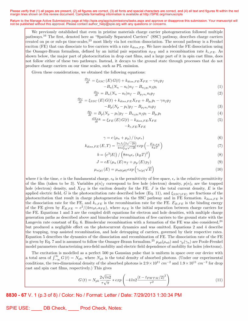
We previously established that even in pristine materials charge carrier photogeneration followed multiplepathways.16 The first, denoted here as “Spatially Separated Carriers” (SSC) pathway, describes charge carrierscreated on ps or sub-ps time-scales,23 most likely via hot exciton dissociation. The second pathway is a Frenkelexciton (FE) that can dissociate to free carriers with a rate kdiss,FE . We have modeled the FE dissociation usingthe Onsager-Braun formalism, defined by an initial pair separation aFE and a recombination rate kr,FE . Asshown below, the major part of photoexcitation in drop cast films, and a large part of it in spin cast films, doesnot follow either of these two pathways. Instead, it decays to the ground state through processes that do notproduce charge carriers on our time scales, such as PL emission.
Given these considerations, we obtained the following equations:
where t is the time, e is the fundamental charge, ε0 is the permittivity of free space, εr is the relative permittivityof the film (taken to be 3). Variables p(n)f correspond to free hole (electron) density, p(n)t are the trappedhole (electron) density, and XFE is the exciton density for the FE. J is the total current density, E is theapplied electric field, G is the photoexcitation rate described below (Eq. 11), and ξSSC(FE) are fractions of thephotoexcitation that result in charge photogeneration via the SSC pathway and in FE formation. kdiss,FE isthe dissociation rate for the FE, and kr,FE is the recombination rate for the FE. EB,FE is the binding energyof the FE given by EB,FE = e2/(4πε0εraFE), where aFE is the initial separation between charge carriers forthe FE. Equations 1 and 3 are the coupled drift equations for electron and hole densities, with multiple chargegeneration paths as described above and bimolecular recombination of free carriers to the ground state with theLangevin rate constant of Eq. 6. Bimolecular recombination with a formation of the FE was also considered,24
but produced a negligible effect on the photocurrent dynamics and was omitted. Equations 2 and 4 describethe trapping, trap assisted recombination, and hole detrapping of carriers, governed by their respective rates.Equation 5 describes the dynamics of the dissociation and recombination of FE. The dissociation rate of the FEis given by Eq. 7 and is assumed to follow the Onsager-Braun formalism.25 µp0(µn0) and γp(γn) are Poole-Frenkelmodel parameters characterizing zero-field mobility and electric field dependence of mobility for holes (electrons).
The excitation is modelled as a perfect 500 ps Gaussian pulse that is uniform in space over our device witha total area of
∫∞−∞G (t) = Nph, where Nph is the total density of absorbed photons. (Under our experimental
conditions, the two-dimensional density of the absorbed photons is 2.9×1011 cm−2 and 1.9×1011 cm−2 for dropcast and spin cast films, respectively.) This gives
G (t) = Nph2√ln2
τ√π∗ exp
(−4 ln2
(t− tFWTM/2)2
τ2
)(11)
Please verify that (1) all pages are present, (2) all figures are correct, (3) all fonts and special characters are correct, and (4) all text and figures fit within the redmargin lines shown on this review document. Complete formatting information is available at http://SPIE.org/manuscripts
Return to the Manage Active Submissions page at http://spie.org/app/submissions/tasks.aspx and approve or disapprove this submission. Your manuscript willnot be published without this approval. Please contact [email protected] with any questions or concerns.
8830 - 67 V. 1 (p.3 of 8) / Color: No / Format: Letter / Date: 7/29/2013 1:30:34 PM
SPIE USE: ____ DB Check, ____ Prod Check, Notes:
Parameter (u) Drop cast ADT-TES-F Spin cast ADT-TES-F
µn,0
(cm2 (V s)
−1)
0.093 0.12
µp,0
(cm2 (V s)
−1)
0.60 1.2
γn (cm/V )1/2
1.8× 10⁻³ 2.8× 10⁻⁴
γp (cm/V )1/2
3.1× 10⁻⁴ 5.4× 10⁻⁶
∆ (meV ) 29 24Nn
(cm−3
)7.1× 10¹⁸ 4.8× 10¹⁸
Np(cm−3
)2.8× 10¹⁸ 4.9× 10¹⁷
BnNn(s−1)
5.1× 10¹¹ 7.5× 10¹¹
BpNp(s−1)
3.9× 10¹⁰ 6.5× 10¹⁰
Bnfpt(cm3s−1
)1.4× 10⁻³ 1.8× 10⁻⁴
Bpfnt(cm3s−1
)2.1× 10⁻⁵ 3.1× 10⁻⁷
aFE (nm) 1.18 1.06Table 1. Parameter values extracted from experimental data for drop cast and spin cast ADT-TES-F films using asimulation with a system of Eqs.(1-11). Parameter descriptions are given in the text.
where tFWTM is the full width at a tenth of maximum of the Gaussian pulse and so G (t = 0) = 0.1Gmax whereGmax is the photon density at the laser pulse maximum.
In order to obtain physically meaningful simulation results, realistic initial carrier densities are necessary.16
We considered as our boundary conditions thermionic injection with image charge effects at the electrode-organicinterface.26,27 The injection barriers φpB and φnB for holes and electrons, respectively, were taken to be 0.25 eVand 2.05 eV. We then assumed that the carrier densities had reached a steady state (dp(n)/dt = 0) before thelaser pulse excitation. This allowed us to solve27 for the average densities at t = 0:16
n0f =JDark (E)
eE
e− φnBkBT
µne−
φnB
kBT + µpe−
φpB
kBT
(12)
p0f =JDark (E)
eE
e−
φpB
kBT
µne−
φnB
kBT + µpe−
φpB
kBT
(13)
n0t =(BnNnn
0f
)/(Bnn
0f +Bpfntp
0f
)(14)
p0t =(BpNpp
0f
)/(Bpp
0f +Bnfptn
0f +Bpt
)(15)
where JDark (E) is the measured dark current density at the applied electric field E.
The system of Eqs. 1-11 with initial conditions Eqs. 12-15 was solved numerically in MATLAB using thebuilt in ode15s function. The simulated transients were then fit to the data using the non-linear optimizationpackage NLOPT.28 The fitting was accomplished through minimizing one of two objective functions:
f1 (~x) =∑n
(JData (tn)− JSim (tn, ~x))2
(16)
f2 (~x) =∑m
(1− r2m) (17)
where ~x is the vector input to the simulation function that incorporates all varied parameters of the model,tn is the nth discrete time value, JData (tn) is the experimentally measured total current at tn, JSim (tn, ~x)is the simulated total current at tn, and r2m is the coefficient of determination of the simulated fit for the mthapplied electric field. Using these objective functions, we obtained sets of parameters that describe experimentallymeasured photocurrent transients at all applied electric fields in the studied range.
Please verify that (1) all pages are present, (2) all figures are correct, (3) all fonts and special characters are correct, and (4) all text and figures fit within the redmargin lines shown on this review document. Complete formatting information is available at http://SPIE.org/manuscripts
Return to the Manage Active Submissions page at http://spie.org/app/submissions/tasks.aspx and approve or disapprove this submission. Your manuscript willnot be published without this approval. Please contact [email protected] with any questions or concerns.
8830 - 67 V. 1 (p.4 of 8) / Color: No / Format: Letter / Date: 7/29/2013 1:30:34 PM
SPIE USE: ____ DB Check, ____ Prod Check, Notes:
0
10
20
30
40
50
60
0 5 10 15 20
0
10
20
30
40
50
60
70
0 5 10 15 20
Pho
tocu
rren
t (μ
A)
Time (ns) Time (ns)
80 kV/cm
60 kV/cm
40 kV/cm
50 kV/cm
40 kV/cm
30 kV/cm
(A) (B)
2 μm2 μm
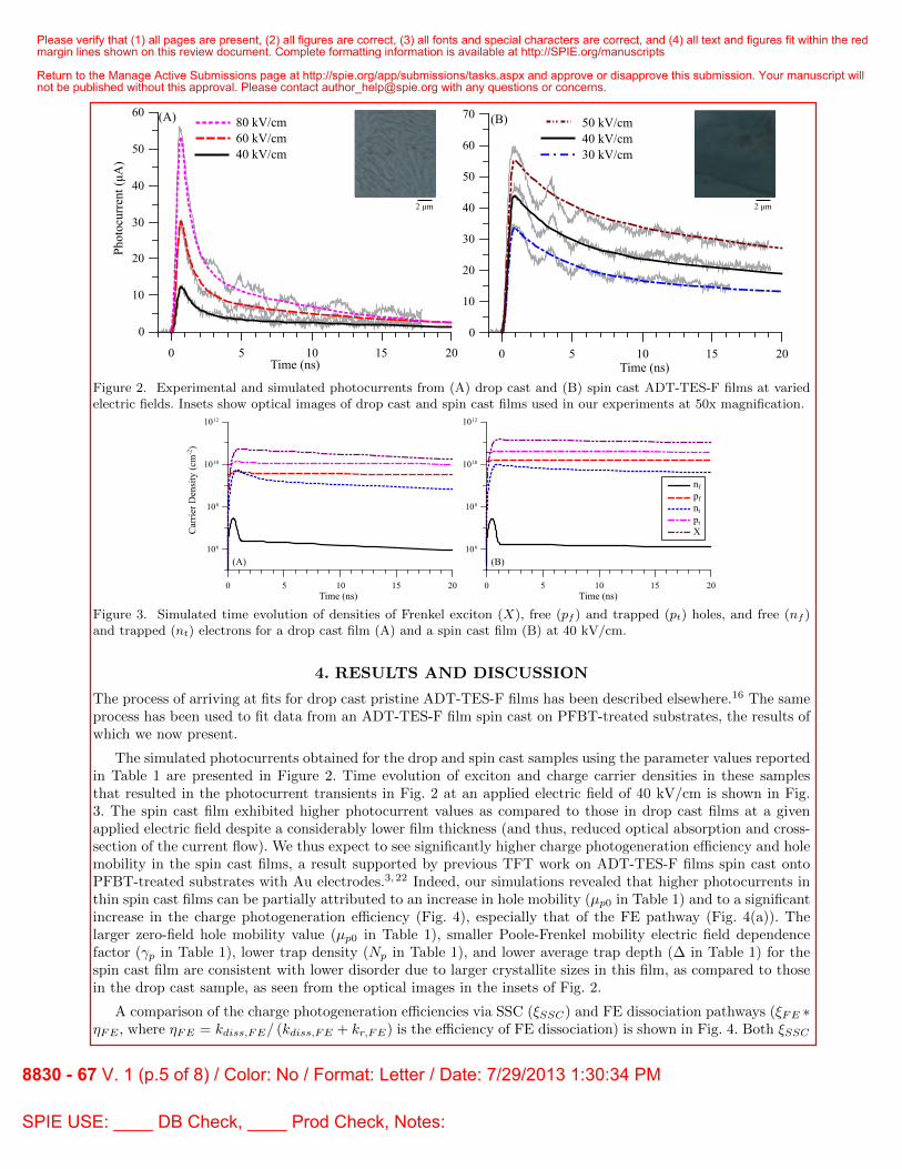
Figure 2. Experimental and simulated photocurrents from (A) drop cast and (B) spin cast ADT-TES-F films at variedelectric fields. Insets show optical images of drop cast and spin cast films used in our experiments at 50x magnification.
106
108
1010
1012
0 5 10 15 20
106
108
1010
1012
0 5 10 15 20
nf
pf
nt
pt
X
(A) (B)
Time (ns) Time (ns)
Car
rier
Den
sity
(cm
-2)
Figure 3. Simulated time evolution of densities of Frenkel exciton (X), free (pf ) and trapped (pt) holes, and free (nf )and trapped (nt) electrons for a drop cast film (A) and a spin cast film (B) at 40 kV/cm.
4. RESULTS AND DISCUSSION
The process of arriving at fits for drop cast pristine ADT-TES-F films has been described elsewhere.16 The sameprocess has been used to fit data from an ADT-TES-F film spin cast on PFBT-treated substrates, the results ofwhich we now present.
The simulated photocurrents obtained for the drop and spin cast samples using the parameter values reportedin Table 1 are presented in Figure 2. Time evolution of exciton and charge carrier densities in these samplesthat resulted in the photocurrent transients in Fig. 2 at an applied electric field of 40 kV/cm is shown in Fig.3. The spin cast film exhibited higher photocurrent values as compared to those in drop cast films at a givenapplied electric field despite a considerably lower film thickness (and thus, reduced optical absorption and cross-section of the current flow). We thus expect to see significantly higher charge photogeneration efficiency and holemobility in the spin cast films, a result supported by previous TFT work on ADT-TES-F films spin cast ontoPFBT-treated substrates with Au electrodes.3,22 Indeed, our simulations revealed that higher photocurrents inthin spin cast films can be partially attributed to an increase in hole mobility (µp0 in Table 1) and to a significantincrease in the charge photogeneration efficiency (Fig. 4), especially that of the FE pathway (Fig. 4(a)). Thelarger zero-field hole mobility value (µp0 in Table 1), smaller Poole-Frenkel mobility electric field dependencefactor (γp in Table 1), lower trap density (Np in Table 1), and lower average trap depth (∆ in Table 1) for thespin cast film are consistent with lower disorder due to larger crystallite sizes in this film, as compared to thosein the drop cast sample, as seen from the optical images in the insets of Fig. 2.
A comparison of the charge photogeneration efficiencies via SSC (ξSSC) and FE dissociation pathways (ξFE ∗ηFE , where ηFE = kdiss,FE/ (kdiss,FE + kr,FE) is the efficiency of FE dissociation) is shown in Fig. 4. Both ξSSC
Please verify that (1) all pages are present, (2) all figures are correct, (3) all fonts and special characters are correct, and (4) all text and figures fit within the redmargin lines shown on this review document. Complete formatting information is available at http://SPIE.org/manuscripts
Return to the Manage Active Submissions page at http://spie.org/app/submissions/tasks.aspx and approve or disapprove this submission. Your manuscript willnot be published without this approval. Please contact [email protected] with any questions or concerns.
8830 - 67 V. 1 (p.5 of 8) / Color: No / Format: Letter / Date: 7/29/2013 1:30:34 PM
SPIE USE: ____ DB Check, ____ Prod Check, Notes:
0.1
0.2
0.3
0.4
0.5
0.6
30 40 50 60 70 80
0.03
0.04
0.05
0.06
0.07
0.08
0.09
30 40 50 60 70 80Electric Field (kV/cm) Electric Field (kV/cm)
ηF
E*ξ F
E
ξ SS
C
Drop Cast
Spin Cast
(A) (B)
Figure 4. A comparison of the (A) FE charge generation pathway efficiency and (B) SSC charge generation pathwayefficiency in spin cast and drop cast ADT-TES-F films.
and ξFE ∗ ηFE were higher in the spin cast film; however, the most pronounced difference between the drop castand spin cast films was in the efficiency of the FE formation ξFE , which was significantly larger in the spin castfilm ( e.g. 79% in the spin cast film, as compared to 20% in the drop cast film, at 40 kV/cm, Fig. 5). Additionally,the simulations revealed that the FE dynamics differed significantly between the drop cast and spin cast films(X in Fig. 3), as the lifetime of the FE in the spin cast film (46− 67 ns, depending on the electric field) was 3-4times longer than that in the drop cast film.16 This suggests that recombination of the charge-generating FE inADT-TES-F films occurs largely at the grain boundaries; it is less efficient in our spin cast film due to its largercrystallite sizes as compared to those in a drop cast film. This is in contrast to the PL-emitting ADT-TES-Fexciton, which exhibits a considerably shorter PL lifetime in spin cast films29 as compared to drop cast films,4,21
and properties of which are related to exciton delocalization within the crystallite.17
The total amount of charge generated at ns time scales, given by ξSSC + ξFE ∗ ηFE , was higher by a factorof ∼ 3 − 4, depending on the electric field, in the spin cast film. As discussed above, this is mostly due to thedifferences in the FE formation efficiency, whereas the efficiency of FE dissociation, ηFE , was comparable in thespin cast and drop cast samples. A schematic representation of the distribution of photoexcitation among variousrelaxation pathways is shown in Figure 5.
The initial decay of the photocurrent (Fig. 2) in the spin cast sample was much slower than that in thedrop cast sample. Our simulation results indicate that this difference is primarily due to the different chargetrapping and recombination characteristics of the two films (Fig. 3). The free hole-trapped electron trap-assistedrecombination rate Bpfnt is particularly important.16 The considerably lower value of Bpfnt in the spin castfilm indicates that holes are less likely to encounter trapped electrons, and less likely to recombine if they doencounter each other, as compared to that in the drop cast film. This suggests that a large number of trapstates in ADT-TES-F films form on grain boundaries, which are considerably reduced by the PFBT treatmentof the substrate with Au electrodes combined with the spin cast deposition method.22 This manifests in thereduced trap densities Np(n) and the trap-assisted recombination rates Bpfnt(Bnfpt), as well as shallower traps(∆ in Table 1) in the spin cast film as compared to the drop cast film. This process competes with the higherhole mobility causing carriers to encounter traps more often, as evidenced by the values of bulk trapping ratesBnNn and BpNp shown in Table 1. The overall effect is an increased speed of initial charge trapping and slowerrelaxation of the free and trapped charge densities in spin cast films (Fig.3).
5. CONCLUSIONS
We applied a model16 that allows us to quantify the contribution of multiple charge generation pathways tocharge carrier photogeneration, as well as extract parameters that characterize charge transport, to organicsemiconductor films prepared using two different deposition methods: drop casting on an untreated substrateand spin casting on a PFBT-treated substrate. In both films, simulations revealed two competing charge pho-togeneration pathways: fast charge generation on a ps or sub-ps time scale with efficiencies below 10%, andslow charge generation, on the time scale of tens of nanoseconds, with efficiencies of 11-12% in drop cast and of50-60% in spin cast films, depending on the applied electric field. The total charge photogeneration efficiency inthe spin cast sample was 59-67% compared to 14-20% in the drop cast sample, whereas the remaining 33-41%and 80-86%, respectively, of the photoexcitation did not contribute to charge carrier generation on these time
Please verify that (1) all pages are present, (2) all figures are correct, (3) all fonts and special characters are correct, and (4) all text and figures fit within the redmargin lines shown on this review document. Complete formatting information is available at http://SPIE.org/manuscripts
Return to the Manage Active Submissions page at http://spie.org/app/submissions/tasks.aspx and approve or disapprove this submission. Your manuscript willnot be published without this approval. Please contact [email protected] with any questions or concerns.
8830 - 67 V. 1 (p.6 of 8) / Color: No / Format: Letter / Date: 7/29/2013 1:30:34 PM
SPIE USE: ____ DB Check, ____ Prod Check, Notes:
Ultrafast CarrierSeparation
Frenkel Exciton
Drop Cast Spin Cast
3.5% 20%
Recombination
Ultrafast CarrierSeparation
Frenkel Exciton
8.0%79%
Free Carriers Free Carriers
65%56%
Initial Excited State Initial Excited State
100%
76.5% 13%
100%
Figure 5. Flowcharts showing distribution of photoexcitation among various relaxation pathways in drop cast and spincast films. The values of each pathway efficiency are exemplars from the 40 kV/cm fits multiplied by 100%.
scales. The spin cast sample also exhibited higher hole mobilities, lower trap densities, shallower traps, and lowercharge carrier recombination, as compared to those in the drop cast sample. Because of these properties, the spincast film exhibited higher photocurrents than the drop cast film, despite its considerably lower thickness leadingto a lower absorption and cross-section of the current flow.
Acknowledgements
We thank Prof. J.E. Anthony for ADT-TES-F and J. Ward and Prof. O. D. Jurchescu for helpful tips on thePFBT treatment of the substrates. This work was supported by the NSF grants DMR-0748671 (via CAREERprogram) and DMR-1207309.
REFERENCES
1. T. Clarke and J. Durrant, “Charge photogeneration in organic solar cells,” Chem. Rev. 110(11), 6736, 2010.
2. B. Walker, C. Kim, and T.-Q. Nguyen, “Small molecule solution-processed bulk heterojunction solar cells,”Chem. Mat. 23(3), 470, 2011.
3. D. J. Gundlach, J. E. Royer, S. K. Park, S. Subramanian, O. D. Jurchescu, B. H. Hamadani, A. J. Moad, R. J.Kline, L. C. Teague, O. Kirillov, C. A. Richter, J. G. Kushmerick, L. J. Richter, S. R. Parkin, T. N. Jackson,and J. E. Anthony, “Contact-induced crystallinity for high-performance soluble acene-based transistors andcircuits,” Nature Mater. 7(3), 216, 2008.
4. A. D. Platt, J. Day, S. Subramanian, J. E. Anthony, and O. Ostroverkhova, “Optical, fluorescent, and(photo)conductive properties of high-performance functionalized pentacene and anthradithiophene deriva-tives,” J. Phys. Chem. C 113(31), 14006, 2009.
5. H. van Eersel, R. A. J. Janssen, and M. Kemerink, “Mechanism for efficient photoinduced charge separationat disordered organic heterointerfaces,” Adv. Func. Mater. 22(13), 2700, 2012.
6. M. C. Heiber and A. Dhinojwala, “Dynamic monte carlo modeling of exciton dissociation in organic donor-acceptor solar cells.,” J. Chem. Phys. 137(1), 014903, 2012.
7. J. Nelson, “Diffusion-limited recombination in polymer-fullerene blends and its influence on photocurrentcollection,” Phys. Rev. B 67(15), 155209, 2003.
8. C. Soci, D. Moses, Q.-H. Xu, and A. Heeger, “Charge-carrier relaxation dynamics in highly ordered poly(p-phenylene vinylene): Effects of carrier bimolecular recombination and trapping,” Phys. Rev. B 72(24),245204, 2005.
9. L. Kulikovsky, D. Neher, E. Mecher, K. Meerholz, H.-H. Horhold, and O. Ostroverkhova, “Photocurrentdynamics in a poly(phenylene vinylene)-based photorefractive composite,” Phys. Rev. B 69(12), 125216,2004.
10. O. Ostroverkhova and K. D. Singer, “Space-charge dynamics in photorefractive polymers,” J. Appl.Phys. 92(4), 1727, 2002.
11. I. Hwang, C. R. McNeill, and N. C. Greenham, “Drift-diffusion modeling of photocurrent transients in bulkheterojunction solar cells,” J. Appl. Phys. 106(9), 094506, 2009.
Please verify that (1) all pages are present, (2) all figures are correct, (3) all fonts and special characters are correct, and (4) all text and figures fit within the redmargin lines shown on this review document. Complete formatting information is available at http://SPIE.org/manuscripts
Return to the Manage Active Submissions page at http://spie.org/app/submissions/tasks.aspx and approve or disapprove this submission. Your manuscript willnot be published without this approval. Please contact [email protected] with any questions or concerns.
8830 - 67 V. 1 (p.7 of 8) / Color: No / Format: Letter / Date: 7/29/2013 1:30:34 PM
SPIE USE: ____ DB Check, ____ Prod Check, Notes:
12. J.-T. Shieh, C.-H. Liu, H.-F. Meng, S.-R. Tseng, Y.-C. Chao, and S.-F. Horng, “The effect of carrier mobilityin organic solar cells,” J. Appl. Phys. 107(8), 084503, 2010.
13. L. Koster, E. Smits, V. Mihailetchi, and P. Blom, “Device model for the operation of polymer/fullerene bulkheterojunction solar cells,” Phys. Rev. B 72(8), 085205, 2005.
14. T. Kirchartz, B. E. Pieters, K. Taretto, and U. Rau, “Mobility dependent efficiencies of organic bulk het-erojunction solar cells: Surface recombination and charge transfer state distribution,” Phys. Rev. B 80(3),035334, 2009.
15. A. Petersen, A. Ojala, T. Kirchartz, T. Wagner, F. Wrthner, and U. Rau, “Field-dependent exciton disso-ciation in organic heterojunction solar cells,” Phys. Rev. B 85(24), 245208, 2012.
16. B. Johnson, M. Kendrick, and O. Ostroverkhova, “Charge carrier dynamics in organic semiconductors andtheir donor-acceptor composites: numerical modeling of time-resolved photocurrent,” submitted to J. Appl.Phys. , 2013.
17. A. Platt, M. Kendrick, M. Loth, J. Anthony, and O. Ostroverkhova, “Temperature dependence of excitonand charge carrier dynamics in organic thin films,” Phys. Rev. B 84(23), 235209, 2011.
18. W. E. B. Shepherd, A. D. Platt, D. Hofer, O. Ostroverkhova, M. Loth, and J. E. Anthony, “Aggregateformation and its effect on (opto)electronic properties of guest-host organic semiconductors,” Appl. Phys.Lett. 97(16), 163303, 2010.
19. R. J. Kline, S. D. Hudson, X. Zhang, D. J. Gundlach, A. J. Moad, O. D. Jurchescu, T. N. Jackson, S. Sub-ramanian, J. E. Anthony, M. F. Toney, and L. J. Richter, “Controlling the microstructure of solution-processable small molecules in thin-film transistors through substrate chemistry,” Chem. Mat. 23(5), 1194,2011.
20. W. E. B. Shepherd, A. D. Platt, M. J. Kendrick, M. A. Loth, J. E. Anthony, and O. Ostroverkhova, “Energytransfer and exciplex formation and their impact on exciton and charge carrier dynamics in organic films,”J. Phys. Chem. Lett 2(5), 362, 2011.
21. M. J. Kendrick, A. Neunzert, M. M. Payne, B. Purushothaman, B. D. Rose, J. E. Anthony, M. M. Haley, andO. Ostroverkhova, “Formation of the donor-acceptor charge-transfer exciton and its contribution to chargephotogeneration and recombination in small-molecule bulk heterojunctions,” J. Phys. Chem. C 116(34),18108, 2012.
22. J. W. Ward, M. a. Loth, R. J. Kline, M. Coll, C. Ocal, J. E. Anthony, and O. D. Jurchescu, “Tailoredinterfaces for self-patterning organic thin-film transistors,” J. Mat. Chem. 22(36), 19047, 2012.
23. J. Day, S. Subramanian, J. E. Anthony, Z. Lu, R. J. Twieg, and O. Ostroverkhova, “Photoconductivity inorganic thin films: From picoseconds to seconds after excitation,” J. Appl. Phys. 103(12), 123715, 2008.
24. W. Tress, K. Leo, and M. Riede, “Optimum mobility, contact properties, and open-circuit voltage of organicsolar cells: A drift-diffusion simulation study,” Phys. Rev. B 85(15), 155201, 2012.
25. C. Braun, “Electric field assisted dissociation of charge transfer states as a mechanism of photocarrierproduction,” J. Chem. Phys. 80, 4157, 1984.
26. J. Scott and G. Malliaras, “Charge injection and recombination at the metal-organic interface,” Chem. Phys.Lett. 299, 115, 1999.
27. S. Lacic and O. Inganas, “Modeling electrical transport in blend heterojunction organic solar cells,” J. Appl.Phys. 97(12), 124901, 2005.
28. S. G. Johnson. The NLOPT non-linear optimization package, version 2.3, 2012, see www.ab-initio.mit.
edu/nlopt.
29. K. Paudel, B. Johnson, A. Neunzera, M. Thieme, J. Anthony, and O. Ostroverkhova in preparation forsubmission to J. Phys. Chem. C. , 2013.
Please verify that (1) all pages are present, (2) all figures are correct, (3) all fonts and special characters are correct, and (4) all text and figures fit within the redmargin lines shown on this review document. Complete formatting information is available at http://SPIE.org/manuscripts
Return to the Manage Active Submissions page at http://spie.org/app/submissions/tasks.aspx and approve or disapprove this submission. Your manuscript willnot be published without this approval. Please contact [email protected] with any questions or concerns.
8830 - 67 V. 1 (p.8 of 8) / Color: No / Format: Letter / Date: 7/29/2013 1:30:34 PM


![[Nonuniform primary photocurrent spreading in quantum well infrared photoconductors]](https://static.documents.pub/doc/80x56/56813ff8550346895dab28e9/nonuniform-primary-photocurrent-spreading-in-quantum-well-infrared-photoconductors.jpg)


