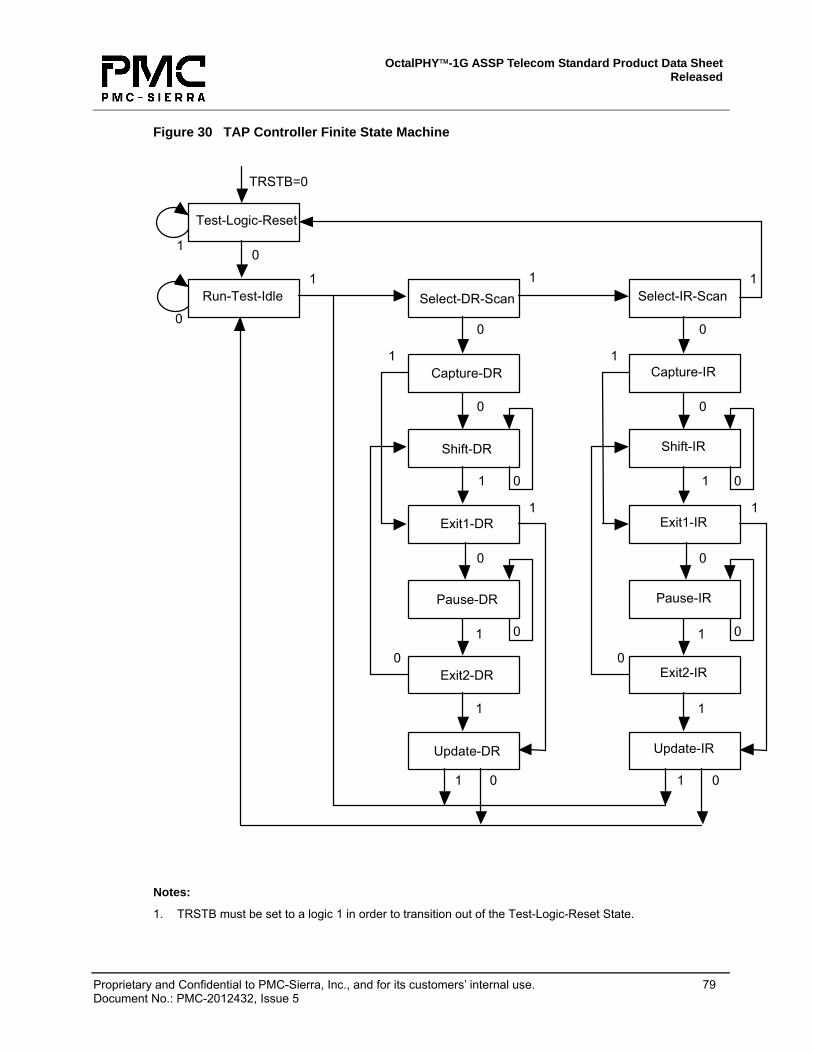
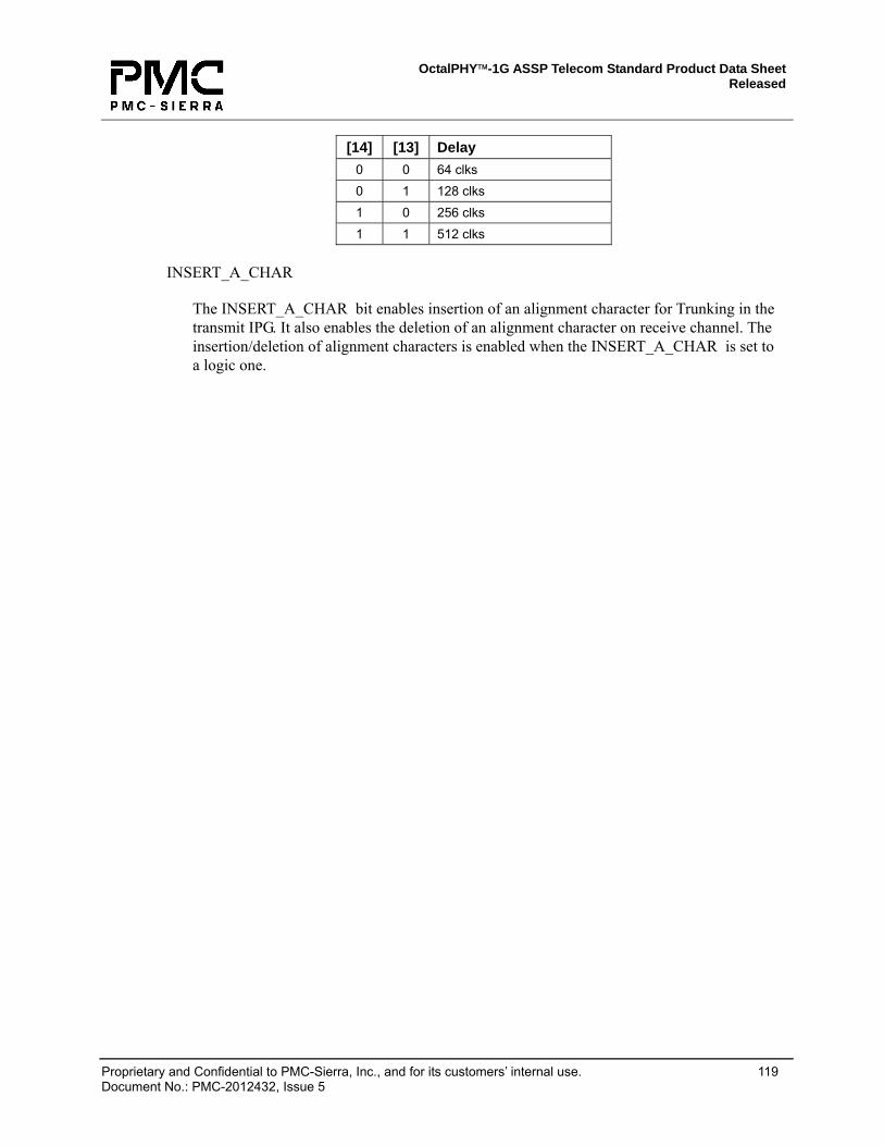
OctalPHY™-1G ASSP Telecom Standard Product Data Sheet Released Proprietary and Confidential to PMC-Sierra, Inc., and for its customers’ internal use. 1 Document No.: PMC-2012432, Issue 5 PM8352 & PM8352A OctalPHY® 1G 8 CHANNEL PHYSICAL LAYER TRANSCEIVER WITH GIGABIT ETHERNET PCS AND TRUNKING FOR 933 Mbit/s TO 1.25 Gbit/s INTERFACES Data Sheet Released Issue No. 5: March 2004
Transcript
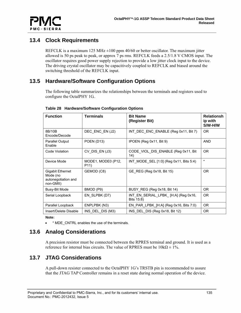
OctalPHY™-1G ASSP Telecom Standard Product Data Sheet Released
Proprietary and Confidential to PMC-Sierra, Inc., and for its customers’ internal use. 1 Document No.: PMC-2012432, Issue 5
PM8352 & PM8352A
OctalPHY® 1G
8 CHANNEL PHYSICAL LAYER TRANSCEIVER WITH GIGABIT ETHERNET PCS AND TRUNKING FOR
933 Mbit/s TO 1.25 Gbit/s INTERFACES
Data Sheet
Released Issue No. 5: March 2004
OctalPHY™-1G ASSP Telecom Standard Product Data Sheet Released
Proprietary and Confidential to PMC-Sierra, Inc., and for its customers’ internal use. 2 Document No.: PMC-2012432, Issue 5
Legal Information
Copyright
Copyright 2004 PMC-Sierra, Inc. All rights reserved.
The information in this document is proprietary and confidential to PMC-Sierra, Inc., and for its customers’ internal use. In any event, no part of this document may be reproduced or redistributed in any form without the express written consent of PMC-Sierra, Inc.
PMC-2012432, R5
Disclaimer
None of the information contained in this document constitutes an express or implied warranty by PMC-Sierra, Inc. as to the sufficiency, fitness or suitability for a particular purpose of any such information or the fitness, or suitability for a particular purpose, merchantability, performance, compatibility with other parts or systems, of any of the products of PMC-Sierra, Inc., or any portion thereof, referred to in this document. PMC-Sierra, Inc. expressly disclaims all representations and warranties of any kind regarding the contents or use of the information, including, but not limited to, express and implied warranties of accuracy, completeness, merchantability, fitness for a particular use, or non-infringement.
In no event will PMC-Sierra, Inc. be liable for any direct, indirect, special, incidental or consequential damages, including, but not limited to, lost profits, lost business or lost data resulting from any use of or reliance upon the information, whether or not PMC-Sierra, Inc. has been advised of the possibility of such damage.
Trademarks
OctalPHY® is a registered trademark of PMC-Sierra, Inc. PMC-Sierra is a trademark of PMC-Sierra, Inc. Other product and company names mentioned herein may be the trademarks of their respective owners.
Patents
Granted
The technology discussed in this document is protected by one or more of the following patent grants:
U.S. Patent No. 6,316,977B1, 6,552,619
OctalPHY™-1G ASSP Telecom Standard Product Data Sheet Released
Proprietary and Confidential to PMC-Sierra, Inc., and for its customers’ internal use. 3 Document No.: PMC-2012432, Issue 5
Contacting PMC-Sierra PMC-Sierra 8555 Baxter Place Burnaby, BC Canada V5A 4V7
OctalPHY™-1G ASSP Telecom Standard Product Data Sheet Released
Proprietary and Confidential to PMC-Sierra, Inc., and for its customers’ internal use. 4 Document No.: PMC-2012432, Issue 5
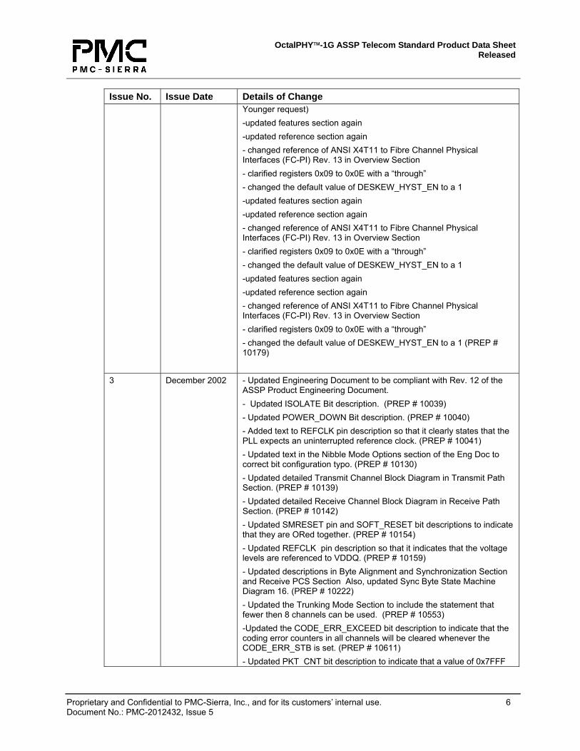
Revision History Issue No. Issue Date Details of Change 1 July 2001 Initial release. 2 May 2002 - Added text to clarify ”Alignment Character insertion during IPG”
description to Receive FIFO Section. - Updated A_DELAY bit description. - Added note to REFCLK to TXCKy AC timing Spec. to clarify description - Added max fall time spec on RESET AC timing Spec. - Added max rise time spec on TRSTB AC timing Spec. - The MDC/MDIO rise and fall times have been changed to max and "Input" has been added to the MDIO rise and fall time description. - Added TzMDIO spec of 10ns. - The JTAG spec is called out in the reference section. The MDC/MDIO interface is called out in Clause 22 of the 802.3 Spec. - Changed Unit from UI in jitter specification to UI pk-pk. Used this interim version to create QuadPHY 1G Eng Doc Issue a3. - Changed the absolute maximum voltage rating on input and bi-directional digital pins in the Absolute Maximum Ratings Section. - Changed Type from R/W to R on the reserved bits in the following registers 0x10, 0x12, 0x13, 0x14, 0x15. - Added AC timing to Parallel Interface section for 106MHz. - Added bit definition table to the INT_MODE_SEL[1:0] bit description in register 0x11. - Added bit definitions to test bits [15:12] of the Redundancy Control Register 0x1D. - Updated the description in the Byte Alignment Section. - Updated Parallel Loopback Section. Removed local clock remote clock relationship description and added modes that are not supported. - Added OUI bit description in the GMII PHY Identifier Register definition. - Changed ANSI X3T11 Fibre Channel compliant to ANSI X3T11 Fibre Channel System compliant in General Feature List. - Updated Transmit Latency Timing Table to account for the increase in the transmit FIFO’s depth. - Added TMS note to TAP Controller Finite State Machine Figure. - Changed item number 5 in the GEMOD pin description. Invalid register location and bit name. - Decreased the pk-pk voltage levels of the High Speed differential outputs in the High-speed I/O Characteristics Table. - Updated sections 20 – 28. - Added Maximum Packet Size - Added implementation section – top level designs - Added implementation section – device level scripts - Updated transmit latency (see TSB PREP #352)
OctalPHY™-1G ASSP Telecom Standard Product Data Sheet Released
Proprietary and Confidential to PMC-Sierra, Inc., and for its customers’ internal use. 5 Document No.: PMC-2012432, Issue 5
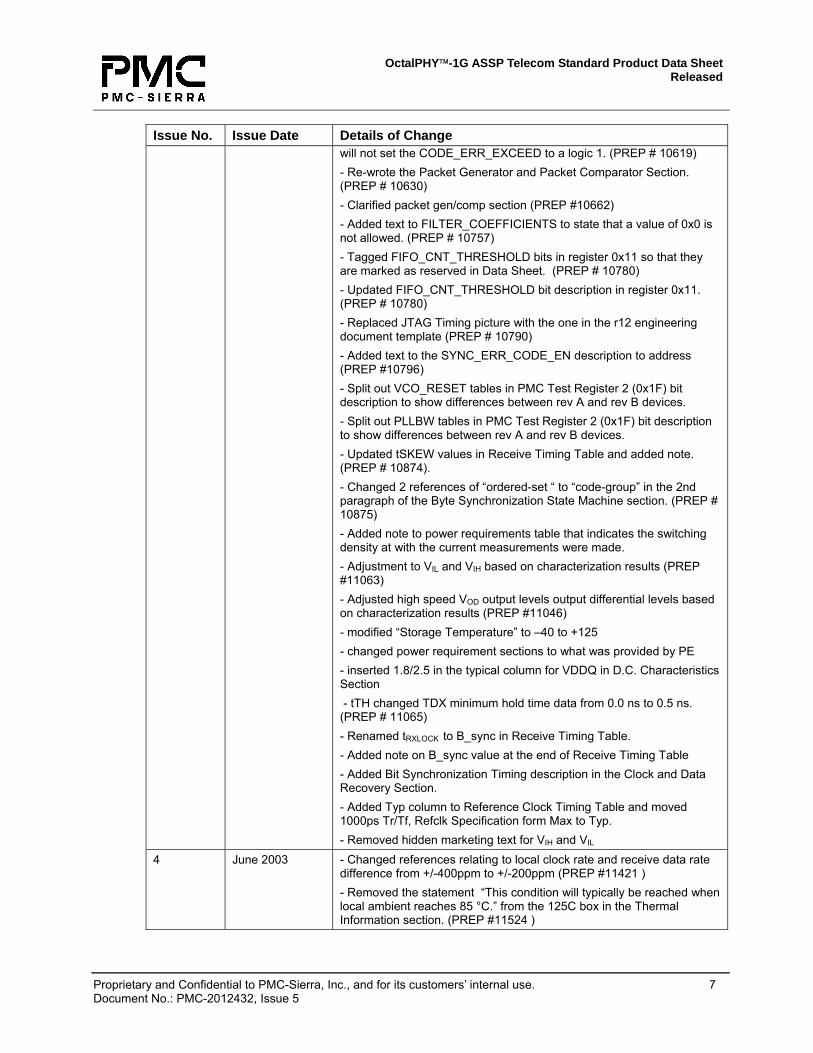
Issue No. Issue Date Details of Change - Added patent section (see Problem Report #8850) - Wrote new description of ST_PKT_DEL_EDGE. - clarified transmit latency (see Problem Report #9386) - fixed typo in Receive Latency Section (see Problem Report #9386 – 2nd part) - added maximum capacitance of MDC/MDIO bus in the “MII Management Interface (MDC/MDIO)” section - Added definition of setup/hold and output delay to the JTAG Port Interface Timing section. - Added input capacitance in low-speed input terminals - commented that the typical numbers will be added once available -Updated DC Characteristics - Changed this table to allow table row changes across multiple pages - In Features/General, changed “Fibre Channel system compliant transceivers” to “Fibre Channel system compatible transceivers” - modified description of “Input, High-speed Differential” pin in Pin Description Section from “…100 Ω” to “…100 ohm differential terminations” - Added how PCS_ENABLE affects RXDxy[9:0] operation in pin description. - Modified the GEMOD pin description - Added note to “Channel Interleave Mode Options Table” - Added note to “Nibble Mode Options Table” - Added Parallel Loopback Option Table - Fixed table cross reference - Changed “8B/10B” to “8B/10B encoder” in Transmit Path Section - Fixed typo “date” -> “data” in transmit path timing - Replaced “occational idle column insert/delete performed” to “IDLE character insertion/deletion for” in Receive Path Section - Prefaced first sentence of 8B/10B section with “When enabled,” - Changed references of PCS_EN to PCS_ENABLE through document - removed “The recovered clock and the REFCLK should be the same frequency within ± 200 ppm.” from the Receive FIFO section as it is described in a following section. - replaced “This 8B decoded data” with “The serial 8B/10B encoded data” in the Gigabit Ethernet and PCS Operating Modes Section - rewrote portions of Gigabit Ethernet and PCS Operating Modes - fixed Note numbering in Tap Controller Section - Made extensive changes to “ST_PKT_DEL_EDGE” - Fixed double note numbering - Removed Differential Returen loss specification per Jim Younger request and Chi approval - Added “output” to High-Speed Serial Timing Characteristics Section - Modified “Reference Clock” table to have a min and max column - Added Power Information Section from latest template (per Jim
OctalPHY™-1G ASSP Telecom Standard Product Data Sheet Released
Proprietary and Confidential to PMC-Sierra, Inc., and for its customers’ internal use. 6 Document No.: PMC-2012432, Issue 5
Issue No. Issue Date Details of Change Younger request) -updated features section again -updated reference section again - changed reference of ANSI X4T11 to Fibre Channel Physical Interfaces (FC-PI) Rev. 13 in Overview Section - clarified registers 0x09 to 0x0E with a “through” - changed the default value of DESKEW_HYST_EN to a 1 -updated features section again -updated reference section again - changed reference of ANSI X4T11 to Fibre Channel Physical Interfaces (FC-PI) Rev. 13 in Overview Section - clarified registers 0x09 to 0x0E with a “through” - changed the default value of DESKEW_HYST_EN to a 1 -updated features section again -updated reference section again - changed reference of ANSI X4T11 to Fibre Channel Physical Interfaces (FC-PI) Rev. 13 in Overview Section - clarified registers 0x09 to 0x0E with a “through” - changed the default value of DESKEW_HYST_EN to a 1 (PREP # 10179)
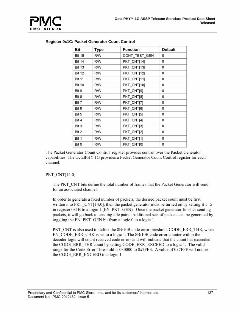
3 December 2002 - Updated Engineering Document to be compliant with Rev. 12 of the ASSP Product Engineering Document. - Updated ISOLATE Bit description. (PREP # 10039) - Updated POWER_DOWN Bit description. (PREP # 10040) - Added text to REFCLK pin description so that it clearly states that the PLL expects an uninterrupted reference clock. (PREP # 10041) - Updated text in the Nibble Mode Options section of the Eng Doc to correct bit configuration typo. (PREP # 10130) - Updated detailed Transmit Channel Block Diagram in Transmit Path Section. (PREP # 10139) - Updated detailed Receive Channel Block Diagram in Receive Path Section. (PREP # 10142) - Updated SMRESET pin and SOFT_RESET bit descriptions to indicate that they are ORed together. (PREP # 10154) - Updated REFCLK pin description so that it indicates that the voltage levels are referenced to VDDQ. (PREP # 10159) - Updated descriptions in Byte Alignment and Synchronization Section and Receive PCS Section Also, updated Sync Byte State Machine Diagram 16. (PREP # 10222) - Updated the Trunking Mode Section to include the statement that fewer then 8 channels can be used. (PREP # 10553) -Updated the CODE_ERR_EXCEED bit description to indicate that the coding error counters in all channels will be cleared whenever the CODE_ERR_STB is set. (PREP # 10611) - Updated PKT_CNT bit description to indicate that a value of 0x7FFF
OctalPHY™-1G ASSP Telecom Standard Product Data Sheet Released
Proprietary and Confidential to PMC-Sierra, Inc., and for its customers’ internal use. 7 Document No.: PMC-2012432, Issue 5
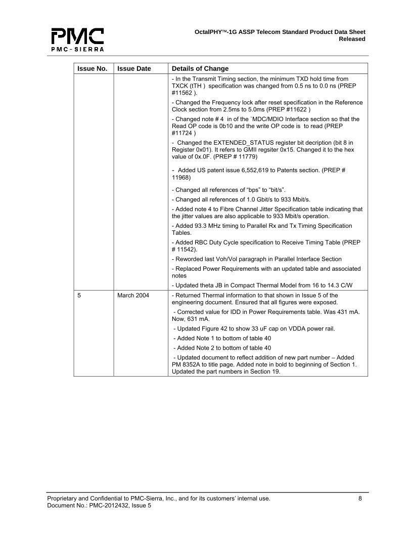
Issue No. Issue Date Details of Change will not set the CODE_ERR_EXCEED to a logic 1. (PREP # 10619) - Re-wrote the Packet Generator and Packet Comparator Section. (PREP # 10630) - Clarified packet gen/comp section (PREP #10662) - Added text to FILTER_COEFFICIENTS to state that a value of 0x0 is not allowed. (PREP # 10757) - Tagged FIFO_CNT_THRESHOLD bits in register 0x11 so that they are marked as reserved in Data Sheet. (PREP # 10780) - Updated FIFO_CNT_THRESHOLD bit description in register 0x11. (PREP # 10780) - Replaced JTAG Timing picture with the one in the r12 engineering document template (PREP # 10790) - Added text to the SYNC_ERR_CODE_EN description to address (PREP #10796) - Split out VCO_RESET tables in PMC Test Register 2 (0x1F) bit description to show differences between rev A and rev B devices. - Split out PLLBW tables in PMC Test Register 2 (0x1F) bit description to show differences between rev A and rev B devices. - Updated tSKEW values in Receive Timing Table and added note. (PREP # 10874). - Changed 2 references of “ordered-set “ to “code-group” in the 2nd paragraph of the Byte Synchronization State Machine section. (PREP # 10875) - Added note to power requirements table that indicates the switching density at with the current measurements were made. - Adjustment to VIL and VIH based on characterization results (PREP #11063) - Adjusted high speed VOD output levels output differential levels based on characterization results (PREP #11046) - modified “Storage Temperature” to –40 to +125 - changed power requirement sections to what was provided by PE - inserted 1.8/2.5 in the typical column for VDDQ in D.C. Characteristics Section - tTH changed TDX minimum hold time data from 0.0 ns to 0.5 ns. (PREP # 11065) - Renamed tRXLOCK to B_sync in Receive Timing Table. - Added note on B_sync value at the end of Receive Timing Table - Added Bit Synchronization Timing description in the Clock and Data Recovery Section. - Added Typ column to Reference Clock Timing Table and moved 1000ps Tr/Tf, Refclk Specification form Max to Typ. - Removed hidden marketing text for VIH and VIL
4 June 2003 - Changed references relating to local clock rate and receive data rate difference from +/-400ppm to +/-200ppm (PREP #11421 ) - Removed the statement “This condition will typically be reached when local ambient reaches 85 °C.” from the 125C box in the Thermal Information section. (PREP #11524 )
OctalPHY™-1G ASSP Telecom Standard Product Data Sheet Released
Proprietary and Confidential to PMC-Sierra, Inc., and for its customers’ internal use. 8 Document No.: PMC-2012432, Issue 5
Issue No. Issue Date Details of Change - In the Transmit Timing section, the minimum TXD hold time from TXCK (tTH ) specification was changed from 0.5 ns to 0.0 ns (PREP #11562 ). - Changed the Frequency lock after reset specification in the Reference Clock section from 2.5ms to 5.0ms (PREP #11622 ) - Changed note # 4 in of the `MDC/MDIO Interface section so that the Read OP code is 0b10 and the write OP code is to read (PREP #11724 ) - Changed the EXTENDED_STATUS register bit decription (bit 8 in Register 0x01). It refers to GMII regsiter 0x15. Changed it to the hex value of 0x.0F. (PREP # 11779)
- Added US patent issue 6,552,619 to Patents section. (PREP # 11968)
- Changed all references of “bps” to “bit/s”. - Changed all references of 1.0 Gbit/s to 933 Mbit/s. - Added note 4 to Fibre Channel Jitter Specification table indicating that the jitter values are also applicable to 933 Mbit/s operation. - Added 93.3 MHz timing to Parallel Rx and Tx Timing Specification Tables. - Added RBC Duty Cycle specification to Receive Timing Table (PREP # 11542). - Reworded last Voh/Vol paragraph in Parallel Interface Section - Replaced Power Requirements with an updated table and associated notes - Updated theta JB in Compact Thermal Model from 16 to 14.3 C/W
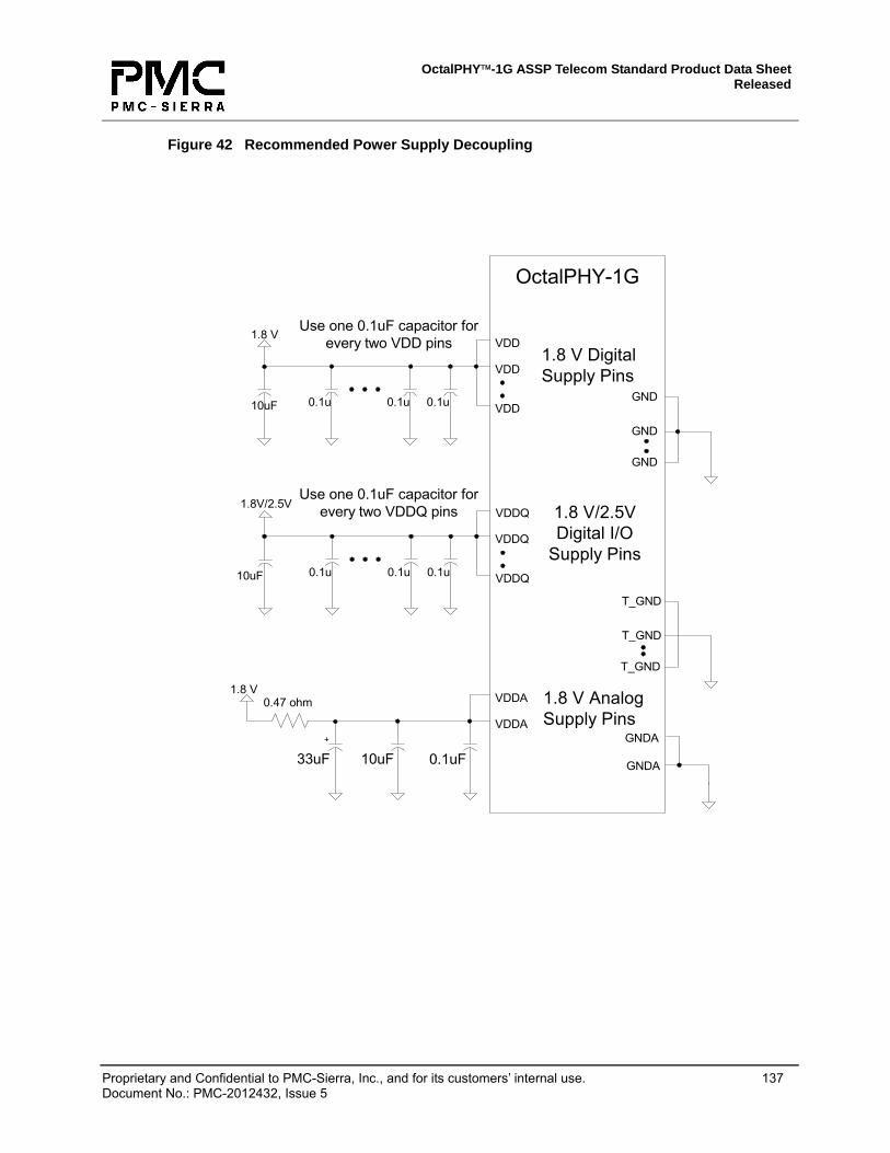
5 March 2004 - Returned Thermal information to that shown in Issue 5 of the engineering document. Ensured that all figures were exposed. - Corrected value for IDD in Power Requirements table. Was 431 mA. Now, 631 mA. - Updated Figure 42 to show 33 uF cap on VDDA power rail. - Added Note 1 to bottom of table 40 - Added Note 2 to bottom of table 40 - Updated document to reflect addition of new part number – Added PM 8352A to title page. Added note in bold to beginning of Section 1. Updated the part numbers in Section 19.
OctalPHY™-1G ASSP Telecom Standard Product Data Sheet Released
Proprietary and Confidential to PMC-Sierra, Inc., and for its customers’ internal use. 9 Document No.: PMC-2012432, Issue 5
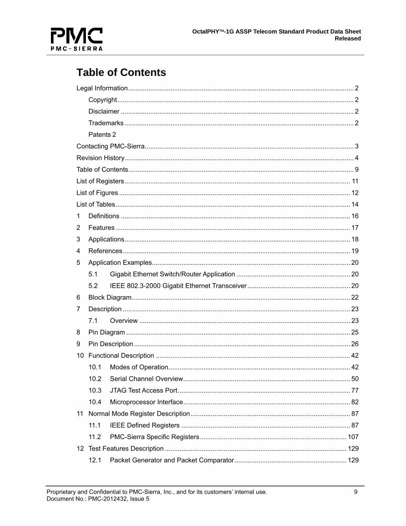
Table of Contents Legal Information........................................................................................................................... 2
10.1 Modes of Operation................................................................................................... 42 10.2 Serial Channel Overview........................................................................................... 50 10.3 JTAG Test Access Port.............................................................................................. 77 10.4 Microprocessor Interface........................................................................................... 82
11 Normal Mode Register Description....................................................................................... 87 11.1 IEEE Defined Registers ............................................................................................ 87 11.2 PMC-Sierra Specific Registers................................................................................ 107
12 Test Features Description ................................................................................................... 129 12.1 Packet Generator and Packet Comparator ............................................................. 129
OctalPHY™-1G ASSP Telecom Standard Product Data Sheet Released
Proprietary and Confidential to PMC-Sierra, Inc., and for its customers’ internal use. 10 Document No.: PMC-2012432, Issue 5
12.2 JTAG Test Access Port............................................................................................ 131 13 Operation ............................................................................................................................ 133
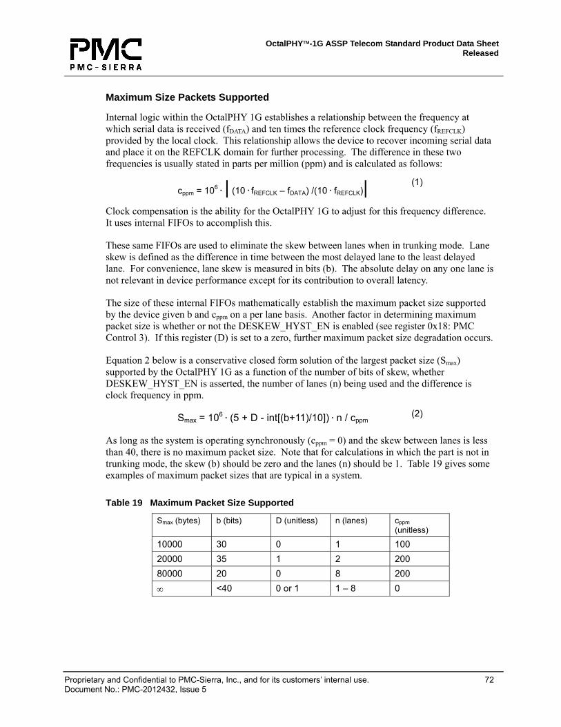
15 Absolute Maximum Ratings ................................................................................................ 140 16 Power Information............................................................................................................... 141
16.1 Power Requirements............................................................................................... 141 16.2 Power Sequencing .................................................................................................. 142 16.3 Power Supply Filtering ............................................................................................ 142
OctalPHY™-1G ASSP Telecom Standard Product Data Sheet Released
Proprietary and Confidential to PMC-Sierra, Inc., and for its customers’ internal use. 11 Document No.: PMC-2012432, Issue 5
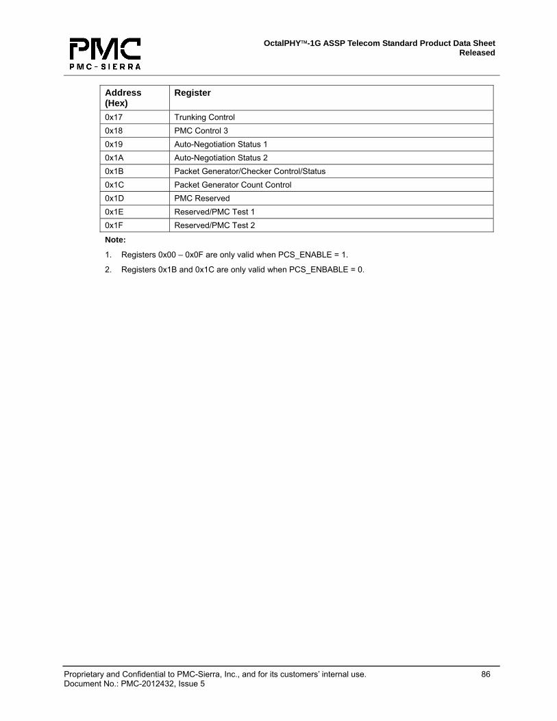
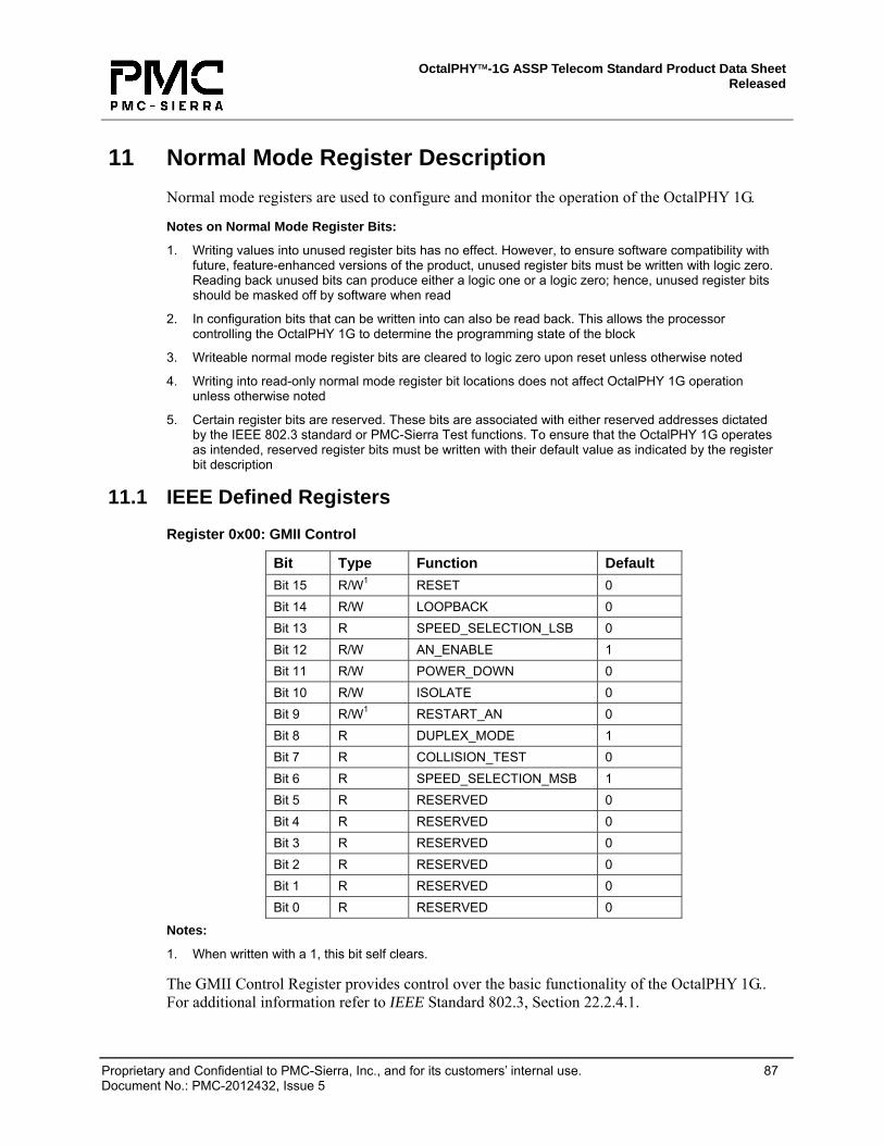
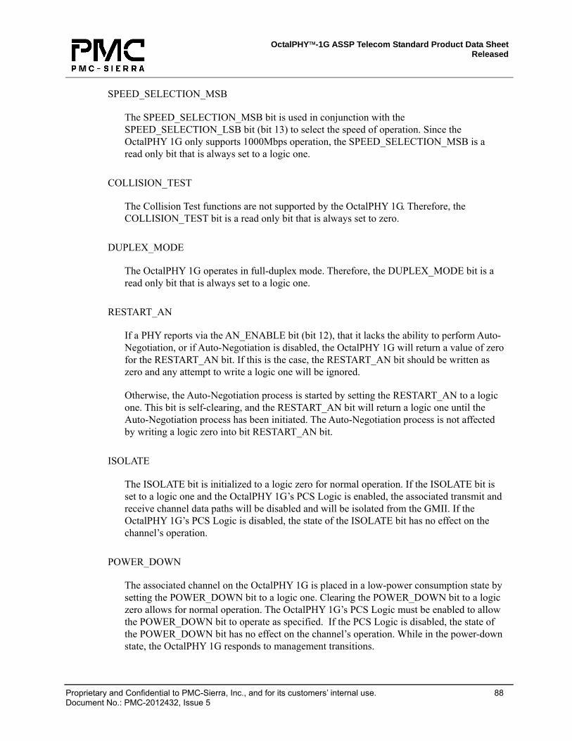
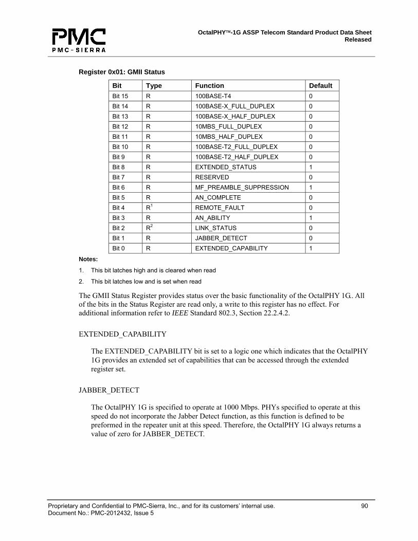
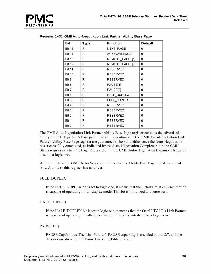
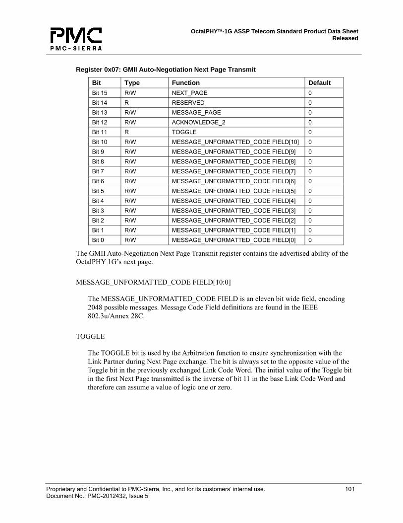
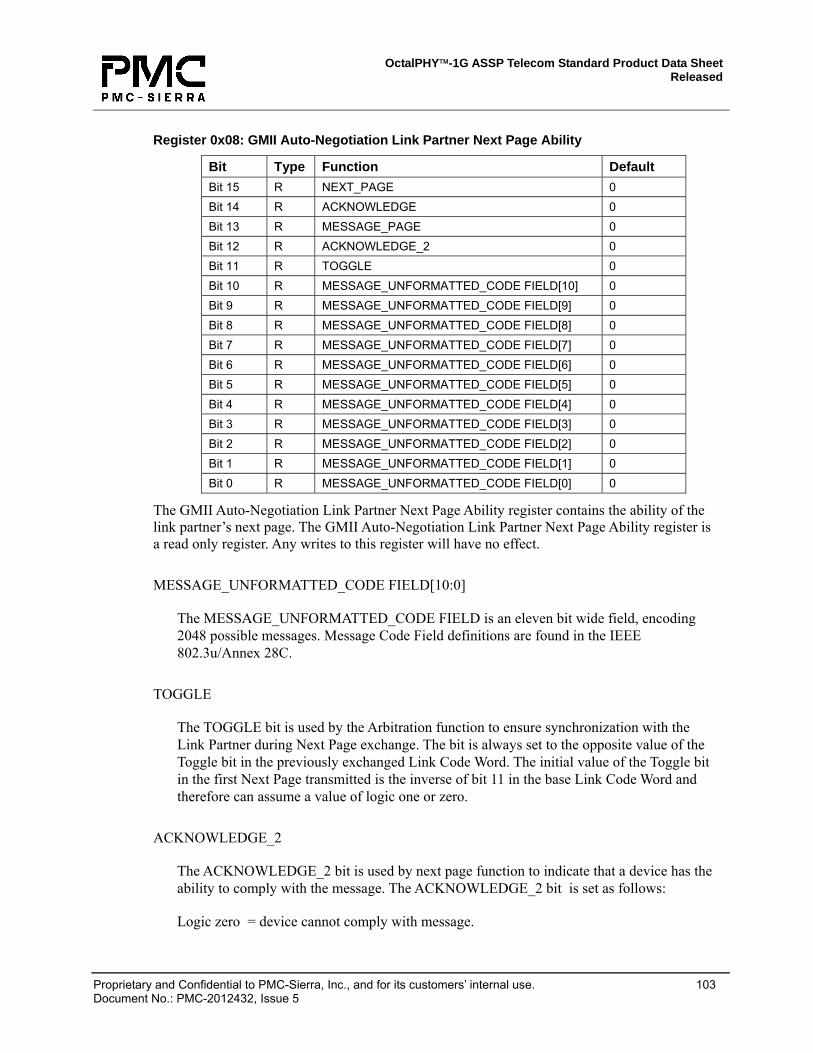
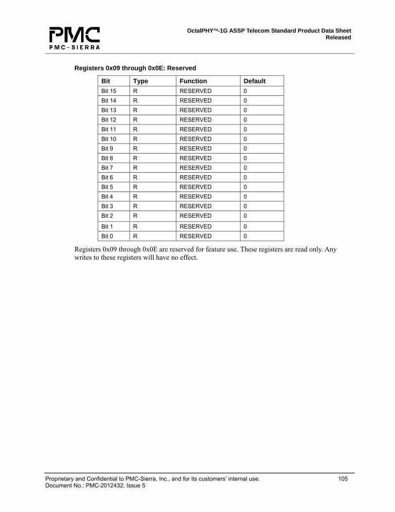
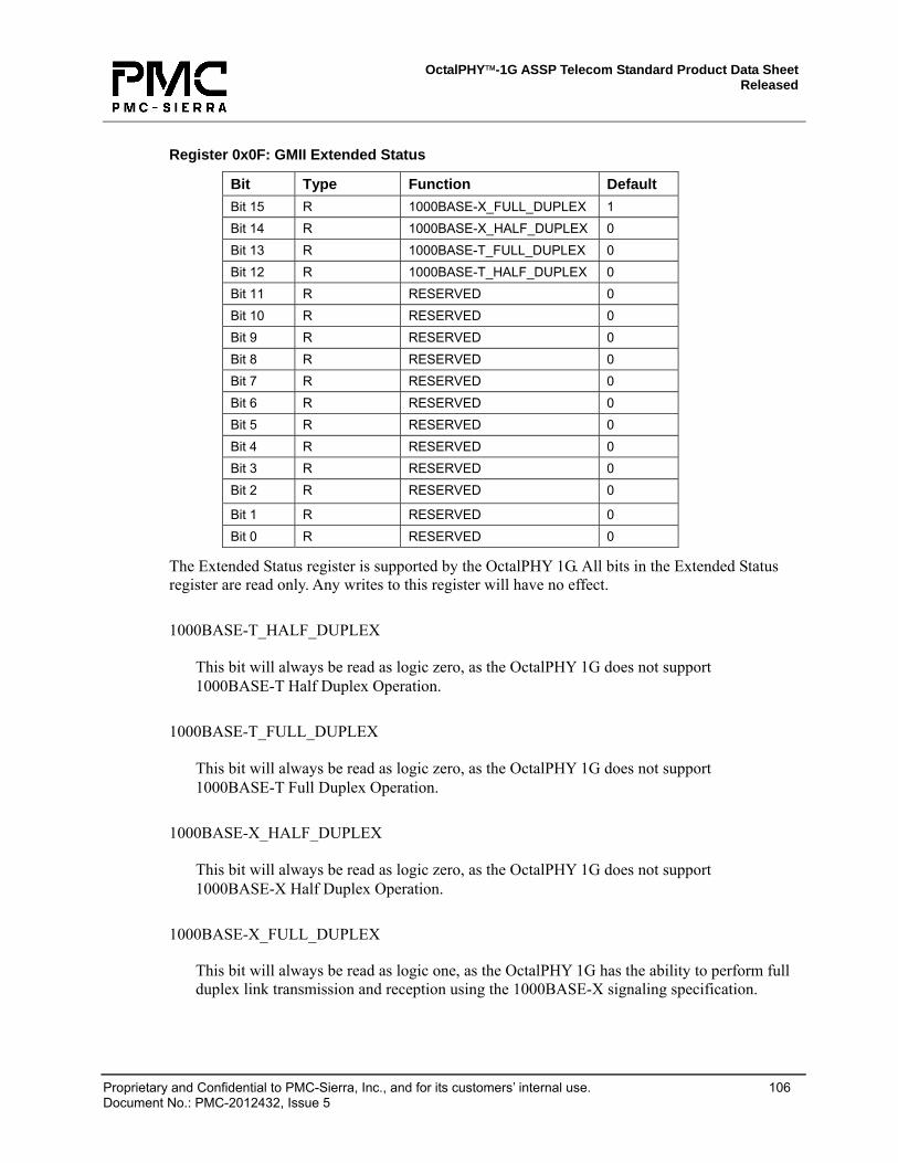
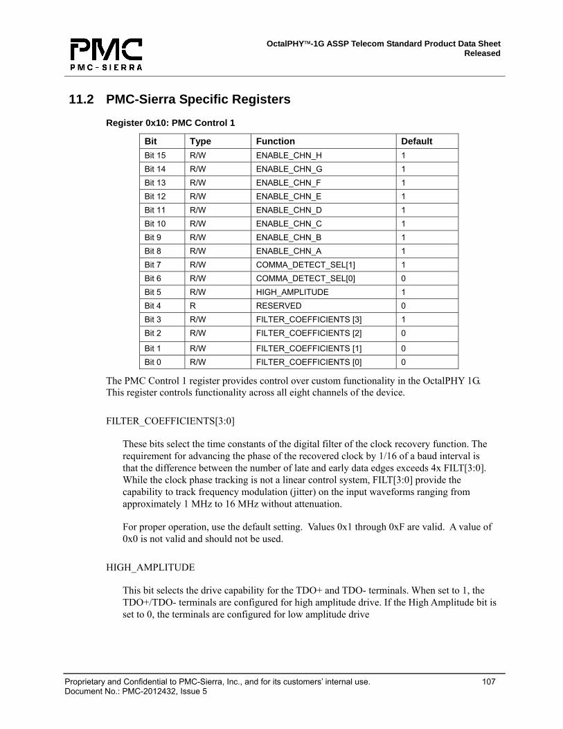
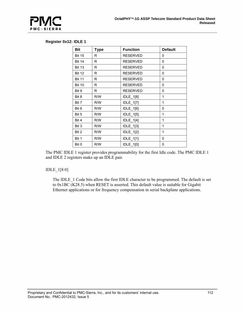
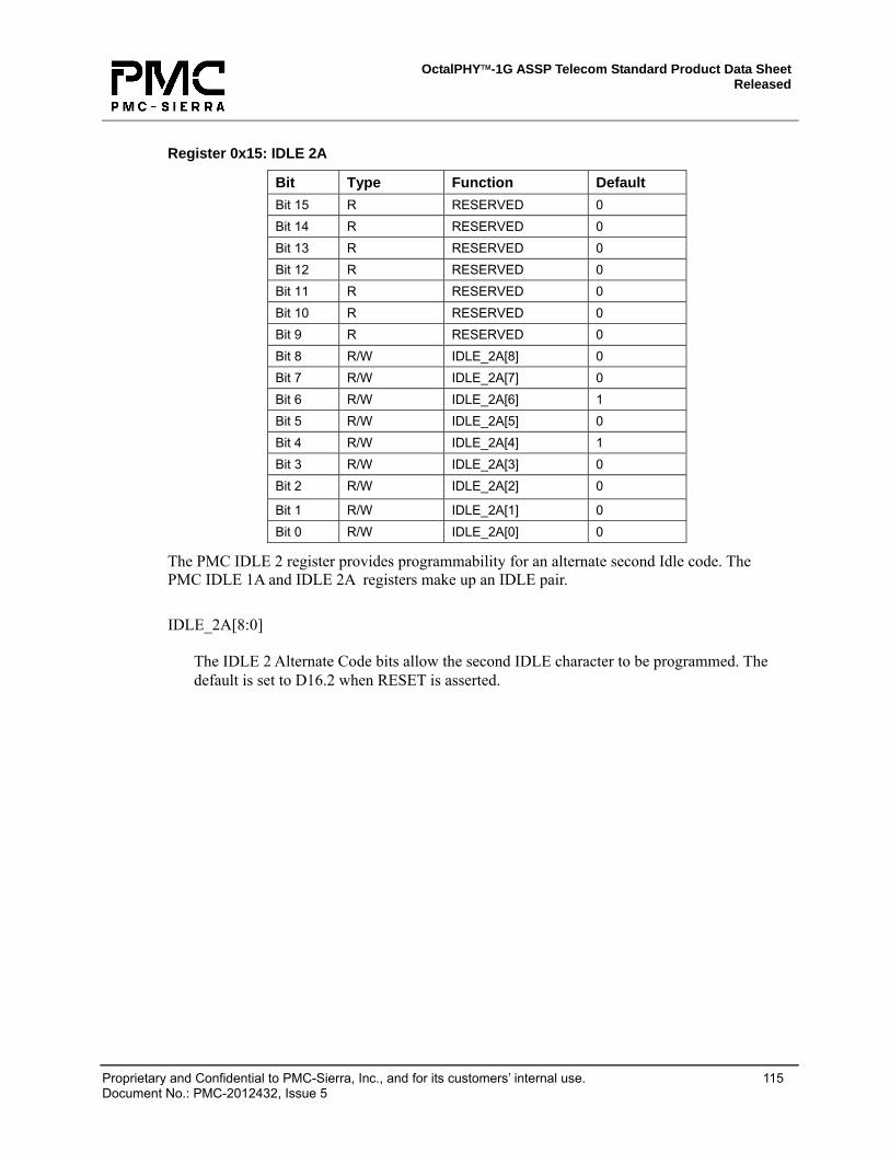
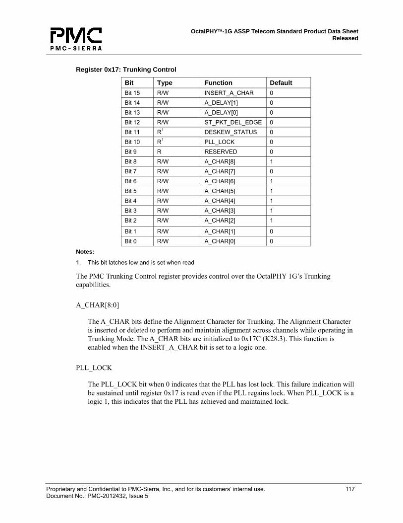
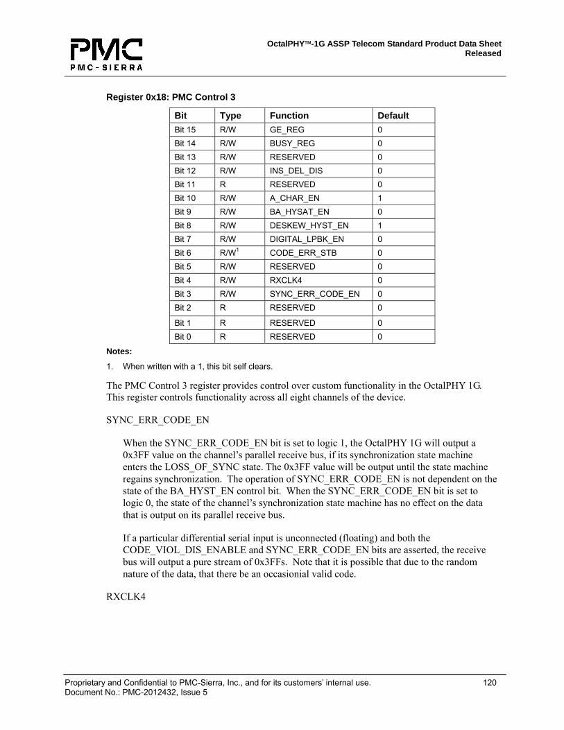
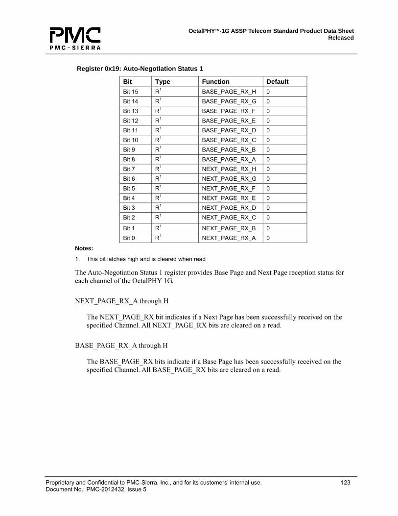
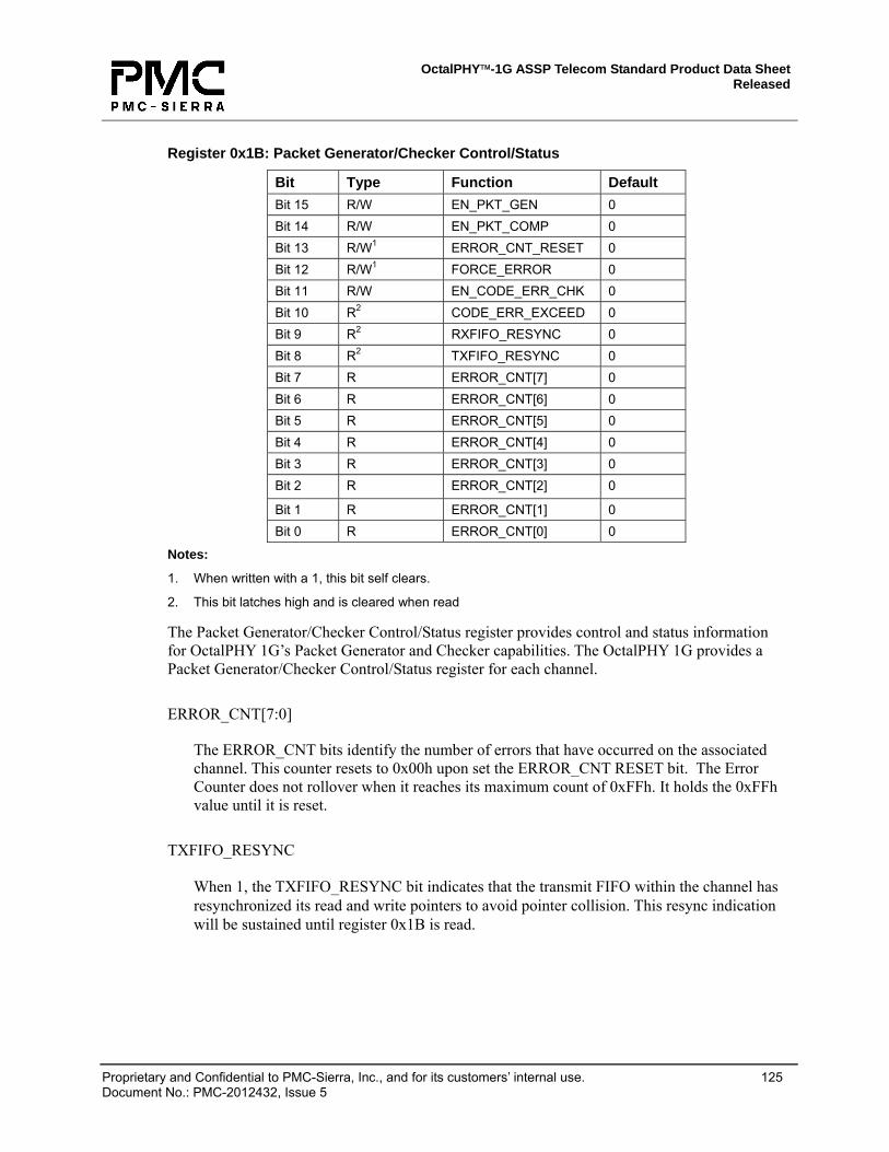
List of Registers Register 0x00: GMII Control ........................................................................................................ 87 Register 0x01: GMII Status ......................................................................................................... 90 Register 0x02: GMII PHY Identifier 1 .......................................................................................... 93 Register 0x03: GMII PHY Identifier 2 .......................................................................................... 95 Register 0x04: GMII Auto-Negotiation Advertisement ................................................................ 96 Register 0x05: GMII Auto-Negotiation Link Partner Ability Base Page....................................... 98 Register 0x06: GMII Auto-Negotiation Expansion..................................................................... 100 Register 0x07: GMII Auto-Negotiation Next Page Transmit...................................................... 101 Register 0x08: GMII Auto-Negotiation Link Partner Next Page Ability ..................................... 103 Registers 0x09 through 0x0E: Reserved................................................................................... 105 Register 0x0F: GMII Extended Status....................................................................................... 106 Register 0x10: PMC Control 1................................................................................................... 107 Register 0x11: PMC Control 2................................................................................................... 109 Register 0x12: IDLE 1 ............................................................................................................... 112 Register 0x13: IDLE 2 ............................................................................................................... 113 Register 0x14: IDLE 1A............................................................................................................. 114 Register 0x15: IDLE 2A............................................................................................................. 115 Register 0x16: Loopback Control .............................................................................................. 116 Register 0x17: Trunking Control................................................................................................ 117 Register 0x18: PMC Control 3................................................................................................... 120 Register 0x19: Auto-Negotiation Status 1 ................................................................................. 123 Register 0x1A: Auto-Negotiation Status 2................................................................................. 124 Register 0x1B: Packet Generator/Checker Control/Status ....................................................... 125 Register 0x1C: Packet Generator Count Control ...................................................................... 127
OctalPHY™-1G ASSP Telecom Standard Product Data Sheet Released
Proprietary and Confidential to PMC-Sierra, Inc., and for its customers’ internal use. 12 Document No.: PMC-2012432, Issue 5
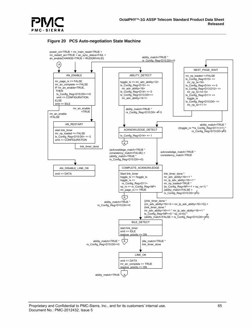
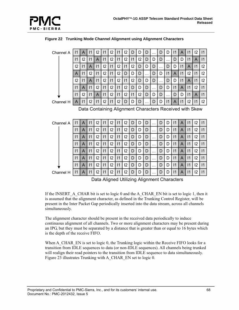
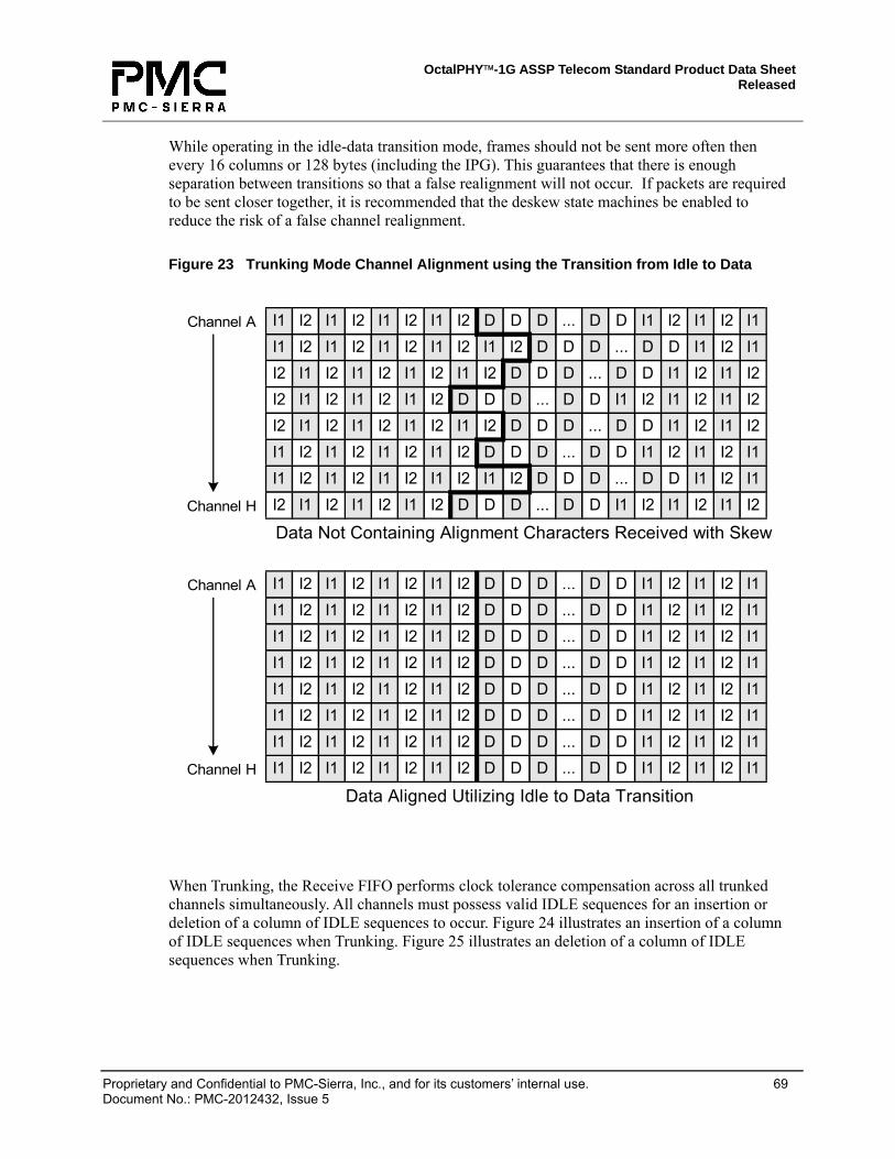
List of Figures Figure 1 OctalPHY 1G in Switch/Router Applications............................................................... 20 Figure 2 IEEE 802.3-2000 Gigabit Ethernet Supported Functions ........................................... 21 Figure 3 OctalPHY 1G Block Diagram ...................................................................................... 22 Figure 4 OctalPHY 1G Detailed Channel Block Diagram ......................................................... 24 Figure 5 OctalPHY 1G Pin Diagram (Bottom View) .................................................................. 25 Figure 6 Interleave Mode Receive Data Path ........................................................................... 43 Figure 7 Nibble Mode Receive Data Path................................................................................. 47 Figure 8 Parallel Loopback Data Path....................................................................................... 49 Figure 9 Transmit Channel Functional Blocks .......................................................................... 53 Figure 10 Transmit Timing for Nibble Mode.............................................................................. 54 Figure 11 Transmit Timing for Channel Interleave Mode.......................................................... 55 Figure 12 Transmit Timing for Trunking Mode .......................................................................... 55 Figure 14 PCS Transmit Code-Group State Machine............................................................... 58 Figure 15 Receive Channel Functional Blocks ......................................................................... 60 Figure 16 Byte Synchronization State Machine ......................................................................... 63 Figure 20 PCS Auto-negotiation State Machine ....................................................................... 65 Figure 21 Insertion/Deletion of Idle Sequences by the Receive FIFO...................................... 66 Figure 22 Trunking Mode Channel Alignment using Alignment Characters ............................. 68 Figure 23 Trunking Mode Channel Alignment using the Transition from Idle to
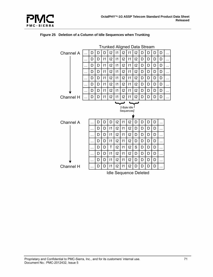
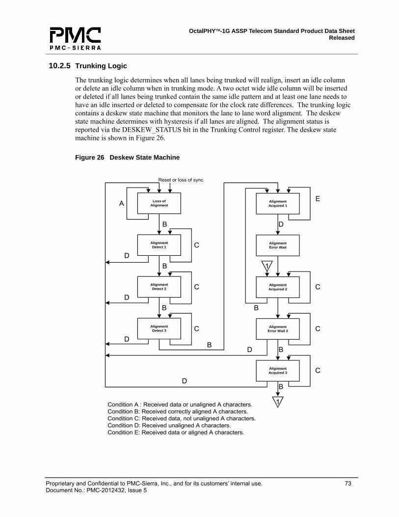
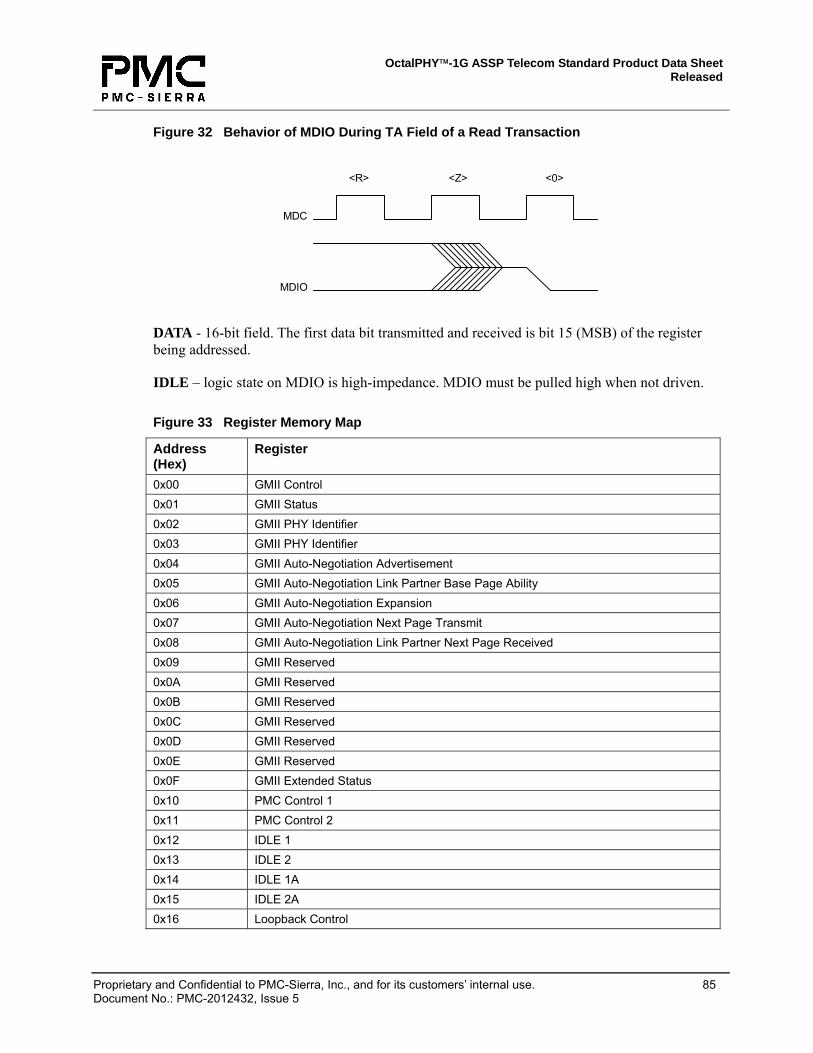
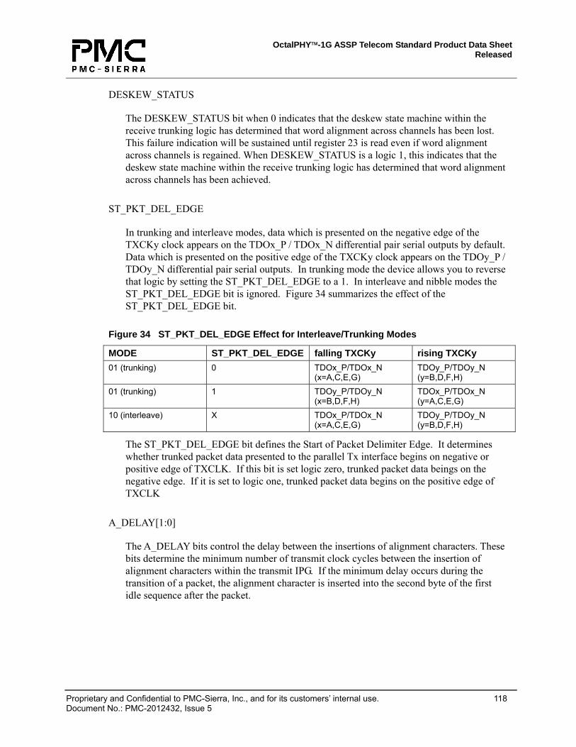
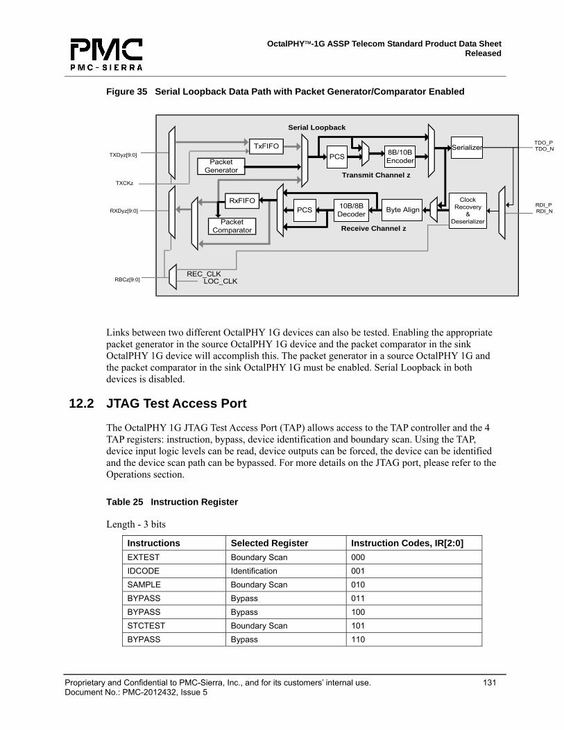
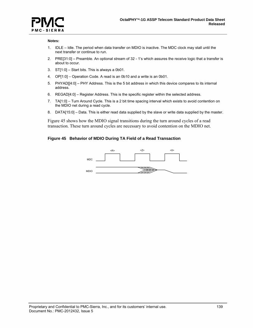
Data....................................................................................................................................... 69 Figure 24 Insertion of a Column of Idle Sequences when Trunking ......................................... 70 Figure 25 Deletion of a Column of Idle Sequences when Trunking.......................................... 71 Figure 26 Deskew State Machine ............................................................................................. 73 Figure 27 Receive Timing for Nibble Mode............................................................................... 75 Figure 28 Receive Timing for Channel Interleaved and Trunked Modes.................................. 76 Figure 29 Boundary Scan Architecture ..................................................................................... 78 Figure 30 TAP Controller Finite State Machine......................................................................... 79 Figure 31 Register Access ........................................................................................................ 83 Figure 32 Behavior of MDIO During TA Field of a Read Transaction....................................... 85 Figure 33 Register Memory Map............................................................................................... 85 Figure 34 ST_PKT_DEL_EDGE Effect for Interleave/Trunking Modes .................................. 118 Figure 35 Serial Loopback Data Path with Packet Generator/Comparator
OctalPHY™-1G ASSP Telecom Standard Product Data Sheet Released
Proprietary and Confidential to PMC-Sierra, Inc., and for its customers’ internal use. 16 Document No.: PMC-2012432, Issue 5
1 Definitions All references to PM8352 in this document denote both PM8352 and PM8352A devices.
The following table defines terms and abbreviations used in this document.
Table 1 Definitions
Term Definition ANSI American National Standards Institute ASIC Application Specific Integrated Circuit BIST Built-in Self Test CABGA Chip Array Ball Grid Array CMOS Complementary Metal-oxide Semiconductor COL Collision Detect. CRS Carrier Sense DDR Dual Data Rate FIFO First In, First Out GMII Gigabit Medium-Independent Interface IEEE Institute of Electrical and Electronics Engineers IPG Interpacket Gap JTAG Joint Test Action Group MDC/MDIO Management Data Clock/Management Data Input/Output PCS Physical Coding Sublayer
OctalPHY™-1G ASSP Telecom Standard Product Data Sheet Released
Proprietary and Confidential to PMC-Sierra, Inc., and for its customers’ internal use. 17 Document No.: PMC-2012432, Issue 5
2 Features General
• Eight 933 Mbit/s to 1.25 Gbit/s IEEE 802.3-2000 Gigabit Ethernet and Fibre Channel Physical Interfaces (FC-PI) System Compliant Transceivers
• Configurable as eight independent channels or as a single logical trunked channel with deskew providing up to 16 Gbit/s duplex data rate throughput.
• Rate matching via IDLE character insertion and deletion capable of compensating up to ±200 ppm of difference between the local REFCLK and the incoming data
• Pin programmable or software configurable operation using 2 pin IEEE 802.3 MDC/MDIO serial management interface
• Ultra-low power operation using 0.18µ technology
Serial Interface
• High-speed outputs feature programmable output current to optimize drive distance and power - directly drives 50 Ω (100 Ω differential) systems
• Direct AC coupled interface to copper serial backplanes, optics and coaxial cable
4. IEEE 1149.1-2001 Standard Test Access Port and Boundary Scan Architecture, 23 July 2001.
5. PMC-2012432, Gigabit OctalPHY 1G Telecom Standard Product Data Sheet.
6. PMC-2010957, SERDES Device Hot Swap Considerations.
7. Electronic Industries Association. Methodology for the Thermal Measurement of Component Packages (Single Semiconductor Device): EIA/JESD51. December 1995.
8. Electronic Industries Alliance 1999. Integrated Circuit Thermal Test Method Environmental Conditions -Junction-to-Board: JESD51-8. October 1999.
9. Telcordia Technologies. Network Equipment-Building System (NEBS) Requirements: Physical Protection: Telcordia Technologies Generic Requirements GR-63-CORE. Issue 1. October 1995.
10. SEMI (Semiconductor Equipment and Materials International). SEMI G30-88 Test Method for Junction-to-Case Thermal Resistance Measurements of Ceramic Packages. 1988.
OctalPHY™-1G ASSP Telecom Standard Product Data Sheet Released
Proprietary and Confidential to PMC-Sierra, Inc., and for its customers’ internal use. 20 Document No.: PMC-2012432, Issue 5
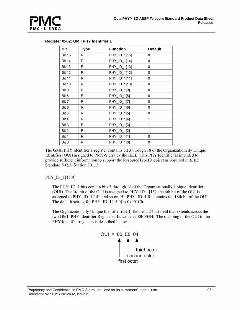
5 Application Examples The OctalPHY 1G has numerous applications in networking, storage and computing systems requiring high-speed serial I/O technology. Typical applications include backplane interconnect, Gigabit Ethernet line cards and Fiber Channel line cards.
5.1 Gigabit Ethernet Switch/Router Application
Figure 1 shows the OctalPHY 1G being used in a Gigabit Ethernet Switch/Router Application. This application demonstrates the many uses of the OctalPHY 1G. On the line cards, the OctalPHY 1G provides the Gigabit Ethernet transceiver function as well as the interface to the backplane. On the switch card, the OctalPHY 1G provides a dense high-speed backplane interconnect to the line cards over a copper backplane.
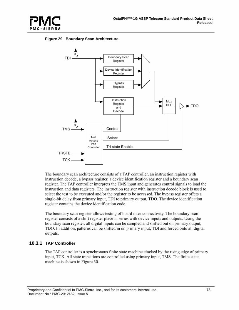
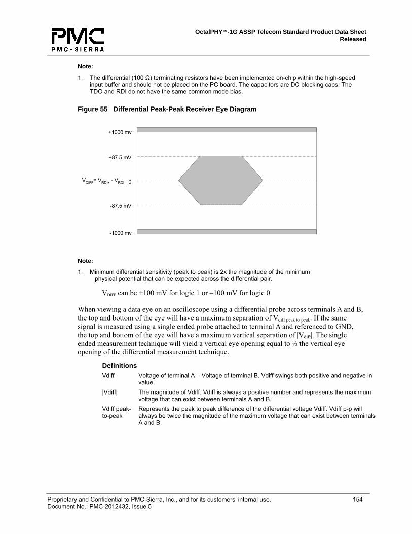
Figure 1 OctalPHY 1G in Switch/Router Applications
8 x 1.25 Gb/s SerialBackplane Links...
...OctalPHY-IG
PM8352
TM
OctalPHY-IG
PM8352
TM
OctalPHY-IG
PM8352
TM
SwitchFabric
8 x GELAN
Optics
8-Port GE Line Card # n
8 OctalPHY-IG
PM8352
TMMACOctalPHY-IG
PM8352
TM
8 x GELAN
Optics
8-Port GE Line Card # 1
8 OctalPHY-IG
PM8352
TMMACOctalPHY-IG
PM8352
TM
HS SerialI/F
ParallelI/F
ParallelI/F
HS SerialI/F
HS SerialI/F
ParallelI/F
ParallelI/F
HS SerialI/F
ParallelI/F
Switch Card
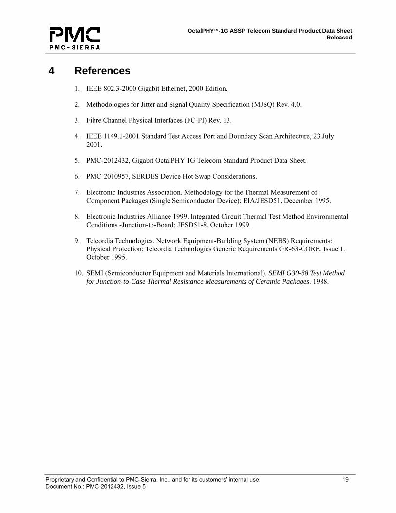
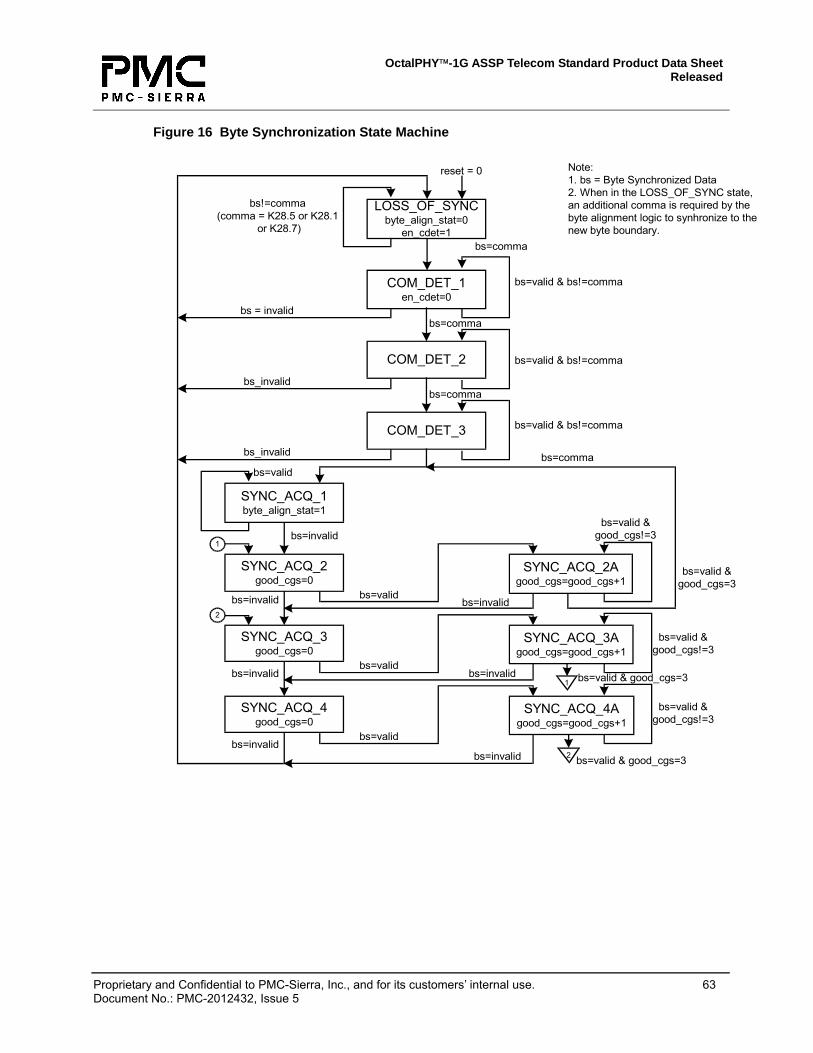
5.2 IEEE 802.3-2000 Gigabit Ethernet Transceiver
As a Gigabit Ethernet Transceiver, the OctalPHY 1G integrates the PCS layer down to the PMA layer for fiber mediums and down to the PMD layer for copper mediums.Figure 2 shows in gray shade, the supported functions of the device. The OctalPHY 1G may be configured to enable or disable certain layers.
OctalPHY™-1G ASSP Telecom Standard Product Data Sheet Released
Proprietary and Confidential to PMC-Sierra, Inc., and for its customers’ internal use. 21 Document No.: PMC-2012432, Issue 5
OctalPHY™-1G ASSP Telecom Standard Product Data Sheet Released
Proprietary and Confidential to PMC-Sierra, Inc., and for its customers’ internal use. 22 Document No.: PMC-2012432, Issue 5
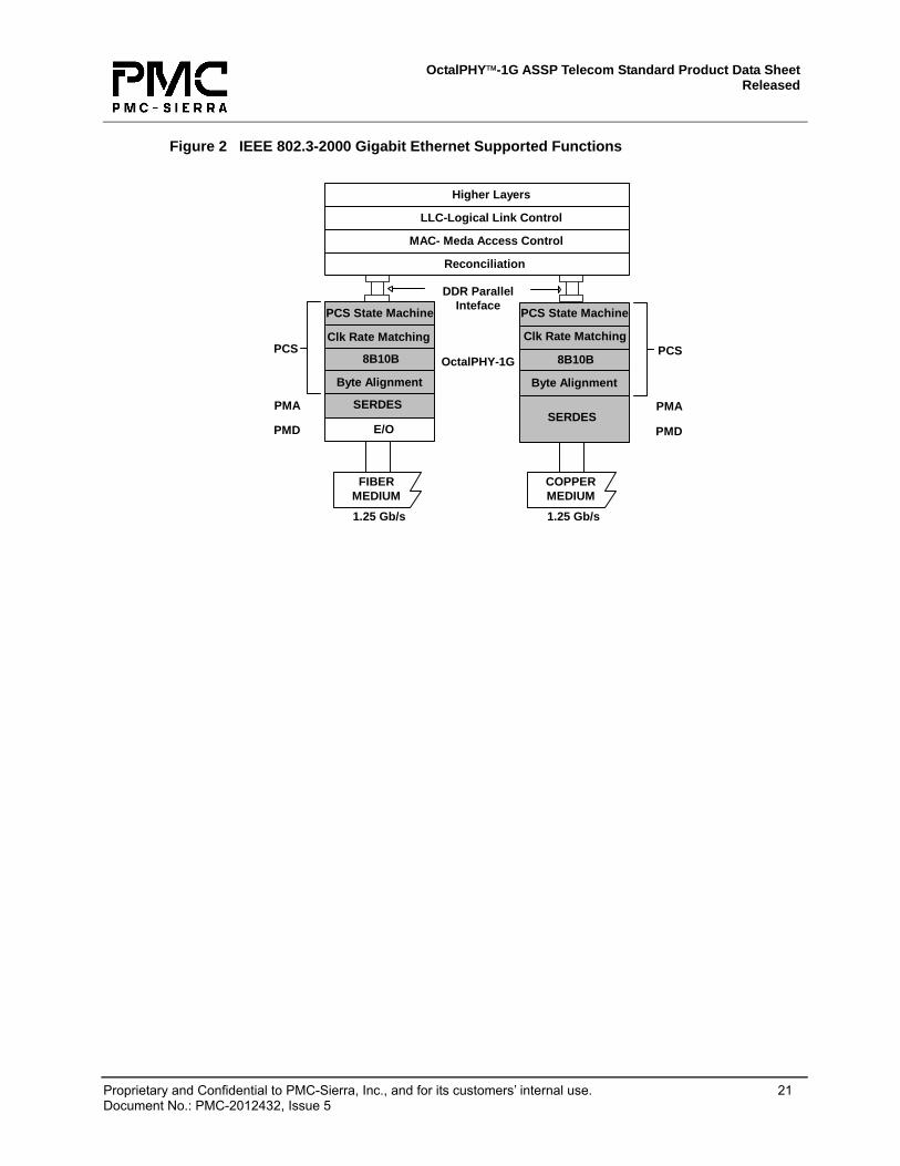
6 Block Diagram The block diagram of the OctalPHY 1G is shown in Figure 3.
Figure 3 OctalPHY 1G Block Diagram
JTAGPLL MDIOI/FControl/Status
REF
CLK
PLL
_LO
CK
TDO
TCK
TDI
TMS
TRST
B
MD
IO
MD
C
DV
AD[4
:0]
CV_
DIS
_EN
DEC
_EN
C_E
NEN
_SLP
BK
GEM
OD
INS_
DEL
_DIS
BMO
DM
OD
E[1:
0]
RES
ET
RPR
ESTDOA_PTDOA_NTXDBA[9:0]
TXCKB
Transmit Channel A
Transmit Channel B TDOB_PTDOB_N
TDOC_PTDOC_NTXDDC[9:0]
TXCKD
Transmit Channel C
Transmit Channel D TDOD_PTDOD_N
TDOE_PTDOE_NTXDFE[9:0]
TXCKF
Transmit Channel E
Transmit Channel F TDOF_PTDOF_N
TDOG_PTDOG_NTXDHG[9:0]
TXCKH
Transmit Channel G
Transmit Channel H Serializer TDOH_PTDOH_N
Serializer
Serializer
Serializer
Serializer
Serializer
Serializer
Serializer
RDIA_PRDIA_NRXDBA[9:0]
RBCBRDIB_PRDIB_N
Clk RecoveryDeserializer
Clk RecoveryDeserializer
RBCA
RDIC_PRDIC_NRXDDC[9:0]
RBCDRDID_PRDID_N
Clk RecoveryDeserializer
Clk RecoveryDeserializer
RBCC
RDIE_PRDIE_NRXDFE[9:0]
RBCFRDIF_PRDIF_N
Clk RecoveryDeserializer
Clk RecoveryDeserializer
RBCE
RDIG_PRDIG_NRXDHG[9:0]
RBCH_H
Receive Channel G
RDIH_PRDIH_N
Clk RecoveryDeserializer
Clk RecoveryDeserializer
RBCG_LRxFIFO
Receive Channel HRxFIFO
Receive Channel ERxFIFO
Receive Channel FRxFIFO
Receive Channel CRxFIFO
Receive Channel DRxFIFO
Receive Channel ARxFIFO
Receive Channel BRxFIFO
EN_P
LPBK
POEN
SMR
ESET
TEST
_EN
OctalPHY™-1G ASSP Telecom Standard Product Data Sheet Released
Proprietary and Confidential to PMC-Sierra, Inc., and for its customers’ internal use. 23 Document No.: PMC-2012432, Issue 5
7 Description
7.1 Overview
The PM8352 OctalPHY 1G is a low power eight channel transceiver suitable for applications such as high-speed serial backplanes and dense Gigabit Ethernet line cards.
In the transmit direction, the PM8352 takes 8-bit or 10-bit data, serializes the data and transmits the data differentially at 933 Mbit/s to1.25 Gbit/s. The PM8352 integrates a DDR parallel interface, 8B/10B encoder, IEEE 802.3-2000 Gigabit Ethernet PCS logic, trunking logic, serializer, clock synthesis unit and differential transmitters.
In the receive direction, the PM8352 receives serial differential data, recovers the data and converts the data back to 8-bit or 10-bit data. The PM8352 integrates differential receivers, clock recovery unit, PCS logic, 8B/10B decoder, receive FIFOs and a DDR parallel interface.
In addition to these fundamental SERDES functions, the PM8352 provides other features such as trunking and rate compensation.
The PM8352 has the ability to trunk data across the eight channels at the transmitter and deskew/realign the data at the receiver. This trunking feature enables the device to provide up to an 8 Gbits/s single logical channel. A system requires deskew due to mismatches in propagation delay between channels. The PM8352 can compensates for this lane-to-lane skewing.
A system requires rate compensation if the transmitting device and receiving device are operating from different clock sources (asynchronous system). For example, if eight asynchronous 1.25 Gbit/s links from eight line cards are transmitting over a backplane to one receiving device, the receiving device must provide rate compensation to achieve a common local clock. The receive logic compensates for these clock differences by inserting or deleting special 8B/10B IDLE characters.
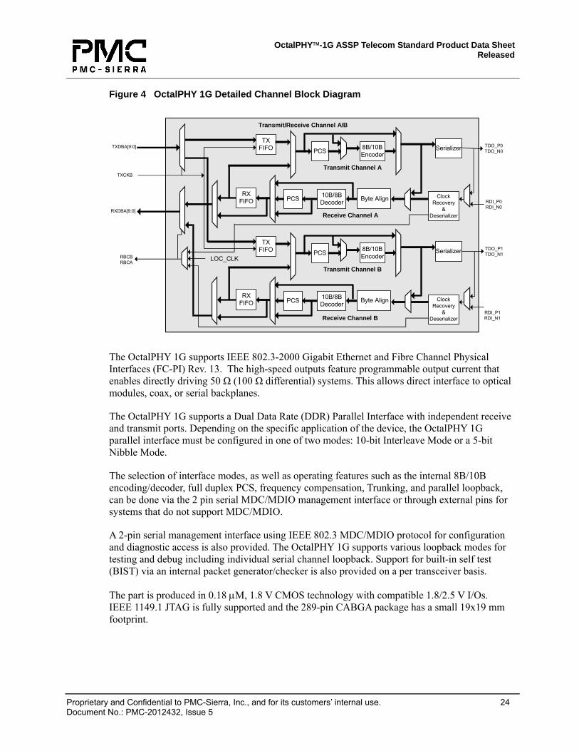
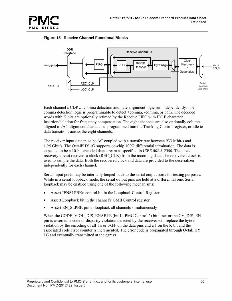
The PM8352 has eight channels (A to H). Figure 4 shows a detailed block diagram of channels A and B. The block diagrams of channels C and D, E and F, and G and H are identical to channels A and B.
OctalPHY™-1G ASSP Telecom Standard Product Data Sheet Released
Proprietary and Confidential to PMC-Sierra, Inc., and for its customers’ internal use. 24 Document No.: PMC-2012432, Issue 5
The OctalPHY 1G supports IEEE 802.3-2000 Gigabit Ethernet and Fibre Channel Physical Interfaces (FC-PI) Rev. 13. The high-speed outputs feature programmable output current that enables directly driving 50 Ω (100 Ω differential) systems. This allows direct interface to optical modules, coax, or serial backplanes.
The OctalPHY 1G supports a Dual Data Rate (DDR) Parallel Interface with independent receive and transmit ports. Depending on the specific application of the device, the OctalPHY 1G parallel interface must be configured in one of two modes: 10-bit Interleave Mode or a 5-bit Nibble Mode.
The selection of interface modes, as well as operating features such as the internal 8B/10B encoding/decoder, full duplex PCS, frequency compensation, Trunking, and parallel loopback, can be done via the 2 pin serial MDC/MDIO management interface or through external pins for systems that do not support MDC/MDIO.
A 2-pin serial management interface using IEEE 802.3 MDC/MDIO protocol for configuration and diagnostic access is also provided. The OctalPHY 1G supports various loopback modes for testing and debug including individual serial channel loopback. Support for built-in self test (BIST) via an internal packet generator/checker is also provided on a per transceiver basis.
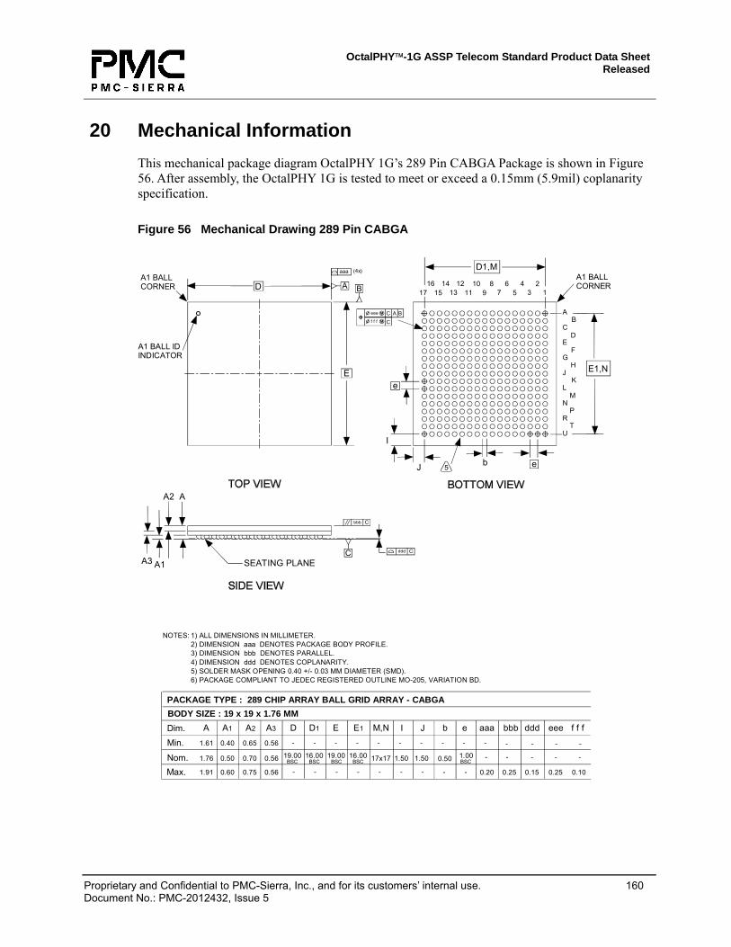
The part is produced in 0.18 µM, 1.8 V CMOS technology with compatible 1.8/2.5 V I/Os. IEEE 1149.1 JTAG is fully supported and the 289-pin CABGA package has a small 19x19 mm footprint.
OctalPHY™-1G ASSP Telecom Standard Product Data Sheet Released
Proprietary and Confidential to PMC-Sierra, Inc., and for its customers’ internal use. 25 Document No.: PMC-2012432, Issue 5
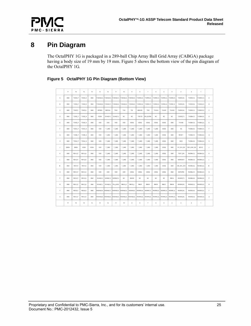
8 Pin Diagram The OctalPHY 1G is packaged in a 289-ball Chip Array Ball Grid Array (CABGA) package having a body size of 19 mm by 19 mm. Figure 5 shows the bottom view of the pin diagram of the OctalPHY 1G.
Figure 5 OctalPHY 1G Pin Diagram (Bottom View)
17 16 15 14 13 12 11 10 9 8 7 6 5 4 3 2 1
A GND TDOH_P TDOH_N GND T XDHG[ 8 ] T XDHG[ 6 ] T XDHG[ 4 ] T XDHG[ 2 ] T XDHG[ 0 ] TXDFE[ 8 ] TXDFE[ 6 ] TXDFE[ 4 ] TXDFE[ 2 ] TXDFE[ 0 ] T XDDC[ 8 ] T XDDC[ 4 ] T XDDC[ 3 ] A
B GND TDOG_P TDOG_N GND T XDHG[ 9 ] T XDHG[ 7 ] T XDHG[ 5 ] T XDHG[ 3 ] TXDHG[ 1] TXDFE[ 9 ] TXDFE[ 7 ] TXDFE[ 5 ] TXDFE[ 3 ] TXDFE[ 1] T XDDC[ 9 ] T XDDC[ 5 ] T XDDC[ 2 ] B
C GND TDOF_P TDOF_N GND RPRES REFCLK T M S TCK TDI GEM OD TDO T XCKH T XCKF T XCKD T XDDC[ 6 ] T XDDC[ 1] T XDDC[ 0 ] C
D GND TDOE_P TDOE_N GND POEN DVAD[ 4 ] DVAD[ 3 ] NC NC T RSTB EN_SLPBK NC NC NC T XDDC[ 7 ] T XDBA[ 1] T XDBA[ 0 ] D
E GND TDOD_P TDOD_N GND VDD VDD VDD VDD VDDQ VDDQ VDDQ VDDQ VDDQ GND TXCKB T XDBA[ 3 ] T XDBA[ 2 ] E
F GND TDOC_P TDOC_N GND VDD T _GND T _GND T _GND T _GND T _GND T _GND T _GND VDDQ GND NC T XDBA[ 5 ] T XDBA[ 4 ] F
G GND TDOB_P TDOB_N GND VDD T _GND T _GND T _GND T _GND T _GND T _GND T _GND VDDQ GND RESET T XDBA[ 7 ] T XDBA[ 6 ] G
H GND TDOA_P TDOA_N GND VDD T _GND T _GND T _GND T _GND T _GND T _GND T _GND VDDQ GND M DC T XDBA[ 9 ] T XDBA[ 8 ] H
J GNDA GNDA VDDA VDDA VDD T _GND T _GND T _GND T _GND T _GND T _GND T _GND VDDQ GND CV_DI S_EN DEC_ENC_EN M DI O J
K GND RDI H_P RDI H_N GND VDD T _GND T _GND T _GND T _GND T _GND T _GND T _GND VDDQ GND TEST _EN RXDBA[ 1] RXDBA[ 0 ] K
L GND RDI G_P RDI G_N GND VDD T _GND T _GND T _GND T _GND T _GND T _GND T _GND VDDQ GND SM RESET RXDBA[ 3 ] RXDBA[ 2 ] L
M GND RDI F_P RDI F_N GND VDD T _GND T _GND T _GND T _GND T _GND T _GND T _GND VDDQ GND I NS_DEL_DI S RXDBA[ 5 ] RXDBA[ 4 ] M
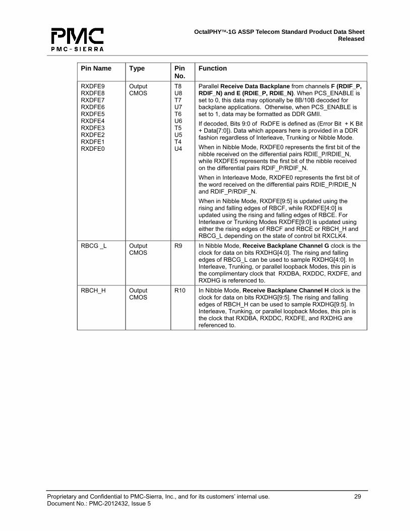
Differential, high-speed serial Receive Data Input pins. This data must be 8B/10B line coded and operate in the range from 933 Mbit/s and 1.25 Gbit/s. The differential inputs are internally terminated with 100 ohm differential terminations. These ports are ignored when Serial Loopback is enabled using either the EN_SLPBK input or the INT_EN_SERIAL_LPBK [H:A] bits in Loopback Register (Register 0x16). These inputs are enabled by default. If a channel is enabled, active data must be provided to it. Do not use pull-up/pull-down resistors on the high-speed differential inputs. These inputs may be left unconnected when this channel is not used .
RBCA Output CMOS
P4 In Nibble Mode, Receive Backplane Channel A clock is the clock for data on bits RXDBA[4:0]. The rising and falling edges of RBCA can be used to sample RXDBA[4:0]. While in Interleave or Trunking Mode, if the RXCLK4 Control Bit (Bit 4 of Register 0x18) is set to a logic 1, the RBCA pin will output the RBCG_L clock. If the RXCLK4 Control Bit is set to a logic 0, the RBCA pin is inactive.
RBCB Output CMOS
R4 In Nibble Mode, Receive Backplane Channel B clock is the clock for data on bits RXDBA[9:5]. The rising and falling edges of RBCB can be used to sample RXDBA[9:5] While in Interleave or Trunking Mode, if the RXCLK4 Control Bit (Bit 4 of Register 0x18) is set to a logic 1, the RBCB pin will output the RBCH_H clock. If the RXCLK4 Control Bit is set to a logic 0, the RBCB pin is inactive.
OctalPHY™-1G ASSP Telecom Standard Product Data Sheet Released
Proprietary and Confidential to PMC-Sierra, Inc., and for its customers’ internal use. 27 Document No.: PMC-2012432, Issue 5
Parallel Receive Data Backplane from channels B (RDIB_P, RDIB_N) and A (RDIA_P, RDIA_N). When PCS_ENABLE is set to 0, this data may optionally be 8B/10B decoded for backplane applications. Otherwise, when PCS_ENABLE is set to 1, data may be formatted as DDR GMII. If decoded, Bits 9:0 of RXDBA are defined as (Error Bit + K Bit + Data[7:0]). Data which appears here is provided in a DDR fashion regardless of Interleave, Trunking or Nibble Mode. When in Nibble Mode, RXDBA0 represents the first bit of the nibble received on the differential pairs RDIA_P/RDIA_N, while RXDBA5 represents the first bit of the nibble received on the differential pairs RDIB_P/RDIB_N. When in Interleave Mode, RXDBA0 represents the first bit of the word received on the differential pairs RDIA_P/RDIA_N and RDIB_P/RDIB_N. When in Nibble Mode, RXDBA[9:5] is updated using the rising and falling edges of RBCB, while RXDBA[4:0] is updated using the rising and falling edges of RBCA. For Interleave or Trunking Modes RXDBA[9:0] is updated using either the rising edges of RBCB and RBCA or RBCH_H and RBCG_L depending on the state of control bit RXCLK4.
RBCC Output CMOS
R5 In Nibble Mode, Receive Backplane Channel C clock is the clock for data on bits RXDDC[4:0]. The rising and falling edges of RBCC can be used to sample RXDDC[4:0]. While in Interleave or Trunking Mode, if the RXCLK4 Control Bit (Bit 4 of Register 0x18) is set to a logic 1, the RBCC pin will output the RBCG_L clock. If the RXCLK4 Control Bit is set to a logic 0, the RBCC pin is inactive.
RBCD Output CMOS
R6 In Nibble Mode, Receive Backplane Channel D clock is the clock for data on bits RXDDC[9:5]. The rising and falling edges of RBCD can be used to sample RXDDC[9:5]. While in Interleave or Trunking Mode, if the RXCLK4 Control Bit (Bit 4 of Register 0x18) is set to a logic 1, the RBCD pin will output the RBCH_H clock. If the RXCLK4 Control Bit is set to a logic 0, the RBCD pin is inactive.
OctalPHY™-1G ASSP Telecom Standard Product Data Sheet Released
Proprietary and Confidential to PMC-Sierra, Inc., and for its customers’ internal use. 28 Document No.: PMC-2012432, Issue 5
Parallel Receive Data Backplane from channels D (RDID_P, RDID_N) and C (RDIC_P, RDIC_N). When PCS_ENABLE is set to 0, this data may optionally be 8B/10B decoded for backplane applications. Otherwise, when PCS_ENABLE is set to 1, data may be formatted as DDR GMII. If decoded, Bits 9:0 of RxDDC is defined as (Error Bit + K Bit + Data[7:0]). Data which appears here is provided in a DDR fashion regardless of Interleave, Trunking or Nibble Mode. When in Nibble Mode, RXDDC0 represents the first bit of the nibble received on the differential pairs RDIC_P/RDIC_N, while RXDDC5 represents the first bit of the nibble received on the differential pairs RDID_P/RDID_N. When in Interleave Mode, RXDDC0 represents the first bit of the word received on the differential pairs RDIC_P/RDIC_N and RDID_P/RDID_N. When in Nibble Mode, RXDDC[9:5] is updated using the rising and falling edges of RBCD, while RXDDC[4:0] is updated using the rising and falling edges of RBCC. For Interleave or Trunking Modes RXDDC[9:0] is updated using either the rising edges of RBCD and RBCC or RBCH_H and RBCG_L depending on the state of control bit RXCLK4.
RBCE Output CMOS
R7 In Nibble Mode, Receive Backplane Channel E clock is the clock for data on bits RXDFE[4:0]. The rising and falling edges of RBCE can be used to sample RXDFE[4:0]. While in Interleave or Trunking Mode, if the RXCLK4 Control Bit (Bit 4 of Register 0x18) is set to a logic 1, the RBCE pin will output the RBCG_L clock. If the RXCLK4 Control Bit is set to a logic 0, the RBCE pin is inactive.
RBCF Output CMOS
R8 In Nibble Mode, Receive Backplane Channel F clock is the clock for data on bits RXDFE[9:5]. The rising and falling edges of RBCF can be used to sample RXDFE[9:5]. While in Interleave or Trunking Mode, if the RXCLK4 Control Bit (Bit 4 of Register 0x18) is set to a logic 1, the RBCF pin will output the RBCH_H clock. If the RXCLK4 Control Bit is set to a logic 0, the RBCF pin is inactive.
OctalPHY™-1G ASSP Telecom Standard Product Data Sheet Released
Proprietary and Confidential to PMC-Sierra, Inc., and for its customers’ internal use. 29 Document No.: PMC-2012432, Issue 5
Parallel Receive Data Backplane from channels F (RDIF_P, RDIF_N) and E (RDIE_P, RDIE_N). When PCS_ENABLE is set to 0, this data may optionally be 8B/10B decoded for backplane applications. Otherwise, when PCS_ENABLE is set to 1, data may be formatted as DDR GMII. If decoded, Bits 9:0 of RxDFE is defined as (Error Bit + K Bit + Data[7:0]). Data which appears here is provided in a DDR fashion regardless of Interleave, Trunking or Nibble Mode. When in Nibble Mode, RXDFE0 represents the first bit of the nibble received on the differential pairs RDIE_P/RDIE_N, while RXDFE5 represents the first bit of the nibble received on the differential pairs RDIF_P/RDIF_N. When in Interleave Mode, RXDFE0 represents the first bit of the word received on the differential pairs RDIE_P/RDIE_N and RDIF_P/RDIF_N. When in Nibble Mode, RXDFE[9:5] is updated using the rising and falling edges of RBCF, while RXDFE[4:0] is updated using the rising and falling edges of RBCE. For Interleave or Trunking Modes RXDFE[9:0] is updated using either the rising edges of RBCF and RBCE or RBCH_H and RBCG_L depending on the state of control bit RXCLK4.
RBCG _L Output CMOS
R9 In Nibble Mode, Receive Backplane Channel G clock is the clock for data on bits RXDHG[4:0]. The rising and falling edges of RBCG_L can be used to sample RXDHG[4:0]. In Interleave, Trunking, or parallel loopback Modes, this pin is the complimentary clock that RXDBA, RXDDC, RXDFE, and RXDHG is referenced to.
RBCH_H Output CMOS
R10 In Nibble Mode, Receive Backplane Channel H clock is the clock for data on bits RXDHG[9:5]. The rising and falling edges of RBCH_H can be used to sample RXDHG[9:5]. In Interleave, Trunking, or parallel loopback Modes, this pin is the clock that RXDBA, RXDDC, RXDFE, and RXDHG are referenced to.
OctalPHY™-1G ASSP Telecom Standard Product Data Sheet Released
Proprietary and Confidential to PMC-Sierra, Inc., and for its customers’ internal use. 30 Document No.: PMC-2012432, Issue 5
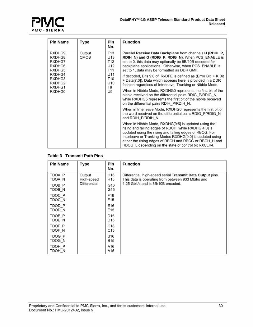
Parallel Receive Data Backplane from channels H (RDIH_P, RDIH_N) and G (RDIG_P, RDIG_N). When PCS_ENABLE is set to 0, this data may optionally be 8B/10B decoded for backplane applications. Otherwise, when PCS_ENABLE is set to 1, data may be formatted as DDR GMII. If decoded, Bits 9:0 of RxDFE is defined as (Error Bit + K Bit + Data[7:0]). Data which appears here is provided in a DDR fashion regardless of Interleave, Trunking or Nibble Mode. When in Nibble Mode, RXDHG0 represents the first bit of the nibble received on the differential pairs RDIG_P/RDIG_N, while RXDHG5 represents the first bit of the nibble received on the differential pairs RDIH_P/RDIH_N. When in Interleave Mode, RXDHG0 represents the first bit of the word received on the differential pairs RDIG_P/RDIG_N and RDIH_P/RDIH_N. When in Nibble Mode, RXDHG[9:5] is updated using the rising and falling edges of RBCH, while RXDHG[4:0] is updated using the rising and falling edges of RBCG. For Interleave or Trunking Modes RXDHG[9:0] is updated using either the rising edges of RBCH and RBCG or RBCH_H and RBCG_L depending on the state of control bit RXCLK4.
Differential, high-speed serial Transmit Data Output pins. This data is operating from between 933 Mbit/s and 1.25 Gbit/s and is 8B/10B encoded.
OctalPHY™-1G ASSP Telecom Standard Product Data Sheet Released
Proprietary and Confidential to PMC-Sierra, Inc., and for its customers’ internal use. 31 Document No.: PMC-2012432, Issue 5
Pin Name Type Pin No.
Function
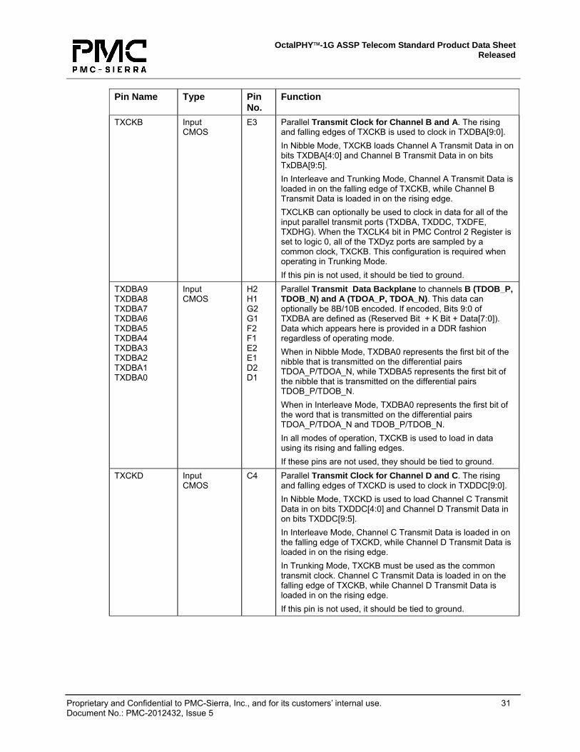
TXCKB Input CMOS
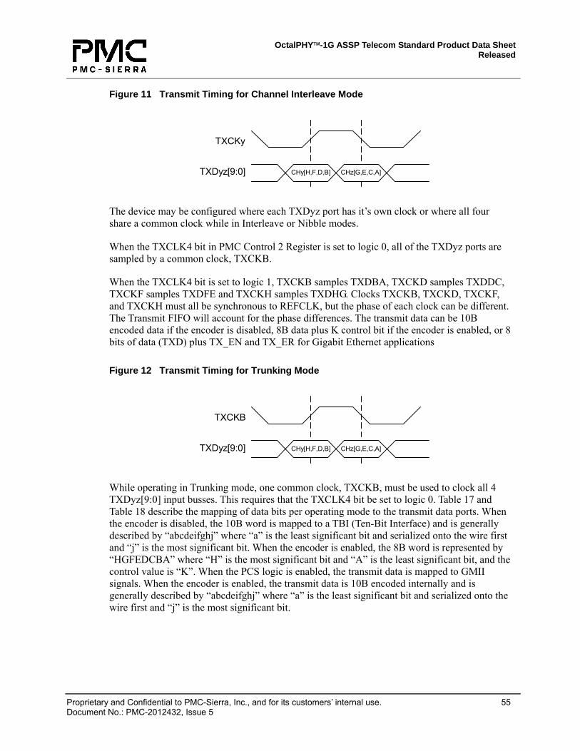
E3 Parallel Transmit Clock for Channel B and A. The rising and falling edges of TXCKB is used to clock in TXDBA[9:0]. In Nibble Mode, TXCKB loads Channel A Transmit Data in on bits TXDBA[4:0] and Channel B Transmit Data in on bits TxDBA[9:5]. In Interleave and Trunking Mode, Channel A Transmit Data is loaded in on the falling edge of TXCKB, while Channel B Transmit Data is loaded in on the rising edge. TXCLKB can optionally be used to clock in data for all of the input parallel transmit ports (TXDBA, TXDDC, TXDFE, TXDHG). When the TXCLK4 bit in PMC Control 2 Register is set to logic 0, all of the TXDyz ports are sampled by a common clock, TXCKB. This configuration is required when operating in Trunking Mode. If this pin is not used, it should be tied to ground.
Parallel Transmit Data Backplane to channels B (TDOB_P, TDOB_N) and A (TDOA_P, TDOA_N). This data can optionally be 8B/10B encoded. If encoded, Bits 9:0 of TXDBA are defined as (Reserved Bit + K Bit + Data[7:0]). Data which appears here is provided in a DDR fashion regardless of operating mode. When in Nibble Mode, TXDBA0 represents the first bit of the nibble that is transmitted on the differential pairs TDOA_P/TDOA_N, while TXDBA5 represents the first bit of the nibble that is transmitted on the differential pairs TDOB_P/TDOB_N. When in Interleave Mode, TXDBA0 represents the first bit of the word that is transmitted on the differential pairs TDOA_P/TDOA_N and TDOB_P/TDOB_N. In all modes of operation, TXCKB is used to load in data using its rising and falling edges. If these pins are not used, they should be tied to ground.
TXCKD Input CMOS
C4 Parallel Transmit Clock for Channel D and C. The rising and falling edges of TXCKD is used to clock in TXDDC[9:0]. In Nibble Mode, TXCKD is used to load Channel C Transmit Data in on bits TXDDC[4:0] and Channel D Transmit Data in on bits TXDDC[9:5]. In Interleave Mode, Channel C Transmit Data is loaded in on the falling edge of TXCKD, while Channel D Transmit Data is loaded in on the rising edge. In Trunking Mode, TXCKB must be used as the common transmit clock. Channel C Transmit Data is loaded in on the falling edge of TXCKB, while Channel D Transmit Data is loaded in on the rising edge. If this pin is not used, it should be tied to ground.
OctalPHY™-1G ASSP Telecom Standard Product Data Sheet Released
Proprietary and Confidential to PMC-Sierra, Inc., and for its customers’ internal use. 32 Document No.: PMC-2012432, Issue 5
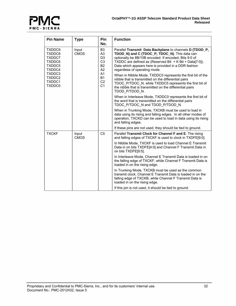
Parallel Transmit Data Backplane to channels D (TDOD_P, TDOD_N) and C (TDOC_P, TDOC_N). This data can optionally be 8B/10B encoded. If encoded, Bits 9:0 of TXDDC are defined as (Reserved Bit + K Bit + Data[7:0]). Data which appears here is provided in a DDR fashion regardless of operating mode. When in Nibble Mode, TXDDC0 represents the first bit of the nibble that is transmitted on the differential pairs TDOC_P/TDOC_N, while TXDDC5 represents the first bit of the nibble that is transmitted on the differential pairs TDOD_P/TDOD_N. When in Interleave Mode, TXDDC0 represents the first bit of the word that is transmitted on the differential pairs TDOC_P/TDOC_N and TDOD_P/TDOD_N. When in Trunking Mode, TXCKB must be used to load in data using its rising and falling edges. In all other modes of operation, TXCKD can be used to load in data using its rising and falling edges. If these pins are not used, they should be tied to ground.
TXCKF Input CMOS
C5 Parallel Transmit Clock for Channel F and E. The rising and falling edges of TXCKF is used to clock in TXDFE[9:0]. In Nibble Mode, TXCKF is used to load Channel E Transmit Data in on bits TXDFE[4:0] and Channel F Transmit Data in on bits TXDFE[9:5]. In Interleave Mode, Channel E Transmit Data is loaded in on the falling edge of TXCKF, while Channel F Transmit Data is loaded in on the rising edge. In Trunking Mode, TXCKB must be used as the common transmit clock. Channel E Transmit Data is loaded in on the falling edge of TXCKB, while Channel F Transmit Data is loaded in on the rising edge. If this pin is not used, it should be tied to ground.
OctalPHY™-1G ASSP Telecom Standard Product Data Sheet Released
Proprietary and Confidential to PMC-Sierra, Inc., and for its customers’ internal use. 33 Document No.: PMC-2012432, Issue 5
Parallel Transmit Data Backplane to channels F (TDOF_P, TDOF_N) and E (TDOE_P, TDOE_N). This data can optionally be 8B/10B encoded. If encoded, Bits 9:0 of TXDFE are defined as (Reserved Bit + K Bit + Data[7:0]). Data which appears here is provided in a DDR fashion regardless of operating mode. When in Nibble Mode, TXDFE0 represents the first bit of the nibble that is transmitted on the differential pairs TDOE_P/TDOE_N, while TXDFE5 represents the first bit of the nibble that is transmitted on the differential pairs TDOF_P/TDOF_N. When in Interleave Mode, TXDFE0 represents the first bit of the word that is transmitted on the differential pairs TDOE_P/TDOE_N and TDOF_P/TDOF_N. When in Trunking Mode, TXCKB must be used to load in data using its rising and falling edges. In all other modes of operation, TXCKF can be used to load in data using its the rising and falling edges. If these pins are not used , they should be tied to ground.
TXCKH Input CMOS
C6 Parallel Transmit Clock for Channel H and G. The rising and falling edges of TXCKH is used to clock in TXDHG[9:0]. In Nibble Mode, TXCKH is used to load Channel G Transmit Data in on bits TXDHG[4:0] and Channel H Transmit Data in on bits TXDHG[9:5]. In Interleave Mode, Channel G Transmit Data is loaded in on the falling edge of TXCKH, while Channel H Transmit Data is loaded in on the rising edge. In Trunking Mode, TXCKB must be used as the common transmit clock. Channel G Transmit Data is loaded in on the falling edge of TXCKB, while Channel H Transmit Data is loaded in on the rising edge. If this pin is not used, it should be tied to ground.
OctalPHY™-1G ASSP Telecom Standard Product Data Sheet Released
Proprietary and Confidential to PMC-Sierra, Inc., and for its customers’ internal use. 34 Document No.: PMC-2012432, Issue 5
Parallel Transmit Data Backplane to channels H (TDOH_P, TDOH_N) and G (TDOG_P, TDOG_N). This data can optionally be 8B/10B encoded. If encoded, Bits 9:0 of TXDHG are defined as (Reserved Bit + K Bit + Data[7:0]). Data which appears here is provided in a DDR fashion regardless of operating mode. When in Nibble Mode, TXDHG0 represents the first bit of the nibble that is transmitted on the differential pairs TDOG_P/TDOG_N, while TXDHG5 represents the first bit of the nibble that is transmitted on the differential pairs TDOH_P/TDOH_N. When in Interleave Mode, TXDHG0 represents the first bit of the word that is transmitted on the differential pairs TDOG_P/TDOG_N and TDOH_P/TDOH_N. When in Trunking Mode, TXCKB must be used to load in data using its rising and falling edges. In all other modes of operation, TXCKH can be used to load in data using its rising and falling edges. If these pins are not used, they should be tied to ground.
Table 4 MDC/MDIO Pins
Pin Name Type Pin No.
Function
DVAD4 DVAD3 DVAD2 DVAD1 DVAD0
Input CMOS
D12 D11 P13 R13 R12
SERDES Device Address. Pins DVAD[4:3] define the base device address of the OctalPHY 1G. Pins DVAD[2:0] are not used and should be tied to logic 0. The MDC/MDIO protocol addresses this device when the 2 MSBs of the PHYAD address match pins DVAD[4:3]. The three LSBs of the MDC/MDIO protocol PHYAD address point to the specific SERDES within the device.
MDIO Input/Output CMOS
J1 Management Data Input/Output. This terminal is the management interface (MI) serial port. During MI write cycles, input data is placed on this terminal and sampled by MDC. During a MI read cycle the MDIO terminal outputs management interface register information. Input data is sampled on the rising edge of MDC. Input and output data on this terminal is referenced to the rising edge of MDC. Note that MDIO should be externally pulled up to VDDQ with a 10kΩ resistor for proper operation between accesses.
MDC Input CMOS
H3 Management Data Clock. Used to control data transfer to/from the management interface registers. Management interface input data is sampled on the rising edges of MDC. When data is to be output on the MDIO terminal it is referenced to the rising edge of MDC. MDC can be aperiodic. The presence of a clock on REFCLK is required for proper operation of the MDC/MDIO interface.
OctalPHY™-1G ASSP Telecom Standard Product Data Sheet Released
Proprietary and Confidential to PMC-Sierra, Inc., and for its customers’ internal use. 35 Document No.: PMC-2012432, Issue 5
Table 5 Configuration/Status Pins
Pin Name Type Pin No.
Function
CV_DIS_EN Input CMOS
J3 Code Violation/Disparity Error Code Enable (Active high). This static signal must be pulled high or low prior to deasserting RESET. Enables the error code option. If a code violation or disparity error is detected, the outputs RXD[9:0] are set to 1. This option requires that the decoder be enabled. This terminal is logically ORed with the CODE_VIOL_DIS_ENABLE bit (Register 0x11).When not asserted, the CV bit indicates the disparity error.
DEC_ENC_EN Input CMOS
J2 Decoder/Encoder Enable (Active high). This static signal must be pulled high or low prior to deasserting RESET. Enables the internal 8B/10B encoder/ decoder across all channels. When set to 0, the device processes 10B encoded data only. This terminal is logically ORed with the INT_DEC_ENC_ENABLE(7) bit (Register 0x11); i.e., the INT_DEC_ENC_ENABLE(7) bit must be low in order for this pin to function.
EN_SLPBK Input CMOS
D7 Enable Serial Data Loop-back (Active high). This static signal must be pulled high or low prior to deasserting RESET. Enables the loop-back function for serial data. When high, serial data is routed from the output of the serializer block to the input of the clock recovery block for each channel. The TDO_P/TDO_N serial outputs are held at a logical 1 state. The RDI_P/RDI_N serial inputs are ignored. Should be held low for normal operation.
SMRESET Input Pulldown CMOS
L3 This active-high State Machine Reset signal provides an asynchronous OctalPHY 1G reset to all state machine flip flops. It has no affect on the PLL or the configuration and status flip flops accessible by the MDC/MDIO port. The minimum reset assertion time is typically less than 500 ns. This terminal is logically ORed with the Soft_Reset bit (Register 0x11) and provides the same functionality.
INS_DEL_DIS Input Pulldown CMOS
M3 Insert/Delete Disable. This static signal must be pulled high or low prior to deasserting RESET. When low, the OctalPHY 1G performs frequency compensation on incoming data. When high, frequency compensation is disabled.
ENPLPBK Input Pulldown CMOS
N3 Enable Parallel Loopback. This static signal must be pulled high or low prior to deasserting RESET. When high, the OctalPHY 1G internally connects all receive channel parallel ports to their corresponding transmit parallel ports. Data is still sent to the parallel outputs. When low, this connection is broken.
OctalPHY™-1G ASSP Telecom Standard Product Data Sheet Released
Proprietary and Confidential to PMC-Sierra, Inc., and for its customers’ internal use. 36 Document No.: PMC-2012432, Issue 5
Pin Name Type Pin No.
Function
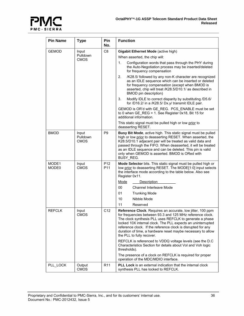
GEMOD Input Pulldown CMOS
C8 Gigabit Ethernet Mode (active high) When asserted, the chip will: 1. Configuration words that pass through the PHY during
the Auto-Negotiation process may be inserted/deleted for frequency compensation
2. /K28.5/ followed by any non-K character are recognized as an IDLE sequence which can be inserted or deleted for frequency compensation (except when BMOD is asserted, chip will treat /K28.5/D10.1/ as described in BMOD pin description)
3. Modify IDLE to correct disparity by substituting /D5.6/ for /D16.2/ in a /K28.5/ Dx.y/ transmit IDLE pair.
GEMOD is OR’d with GE_REG. PCS_ENABLE must be set to 0 when GE_REG = 1. See Register 0x18, Bit 15 for additional information. This static signal must be pulled high or low prior to deasserting RESET.
BMOD Input Pulldown CMOS
P9 Busy Bit Mode, active high. This static signal must be pulled high or low prior to deasserting RESET. When asserted, the K28.5/D10.1 adjacent pair will be treated as valid data and passed through the FIFO. When deasserted, it will be treated as an IDLE sequence and can be deleted. This pin is valid only when GEMOD is asserted. BMOD is ORed with BUSY_REG.
MODE1 MODE0
Input CMOS
P12 P11
Mode Selector bits. This static signal must be pulled high or low prior to deasserting RESET. The MODE[1:0] input selects the interface mode according to the table below. Also see Register 0x11. Mode Description 00 Channel Interleave Mode 01 Trunking Mode 10 Nibble Mode 11 Reserved
REFCLK Input CMOS
C12 Reference Clock. Requires an accurate, low jitter, 100 ppm for frequencies between 93.3 and 125 MHz reference clock. The clock synthesis PLL uses REFCLK to generate a phase locked 10X internal clock. The PLL expects an uninterrupted reference clock. If the reference clock is disrupted for any duration of time, a hardware reset maybe necessary to allow the PLL to fully recover. REFCLK is referenced to VDDQ voltage levels (see the D.C Characteristics Section for details about Vol and Voh logic thresholds). The presence of a clock on REFCLK is required for proper operation of the MDC/MDIO interface.
PLL_LOCK Output CMOS
R11 PLL Lock is an external indication that the internal clock synthesis PLL has locked to REFCLK.
OctalPHY™-1G ASSP Telecom Standard Product Data Sheet Released
Proprietary and Confidential to PMC-Sierra, Inc., and for its customers’ internal use. 37 Document No.: PMC-2012432, Issue 5
Pin Name Type Pin No.
Function
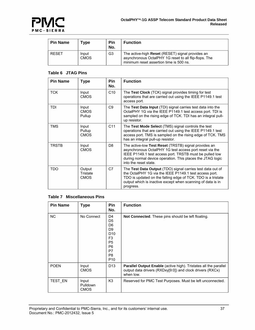
RESET Input CMOS
G3 The active-high Reset (RESET) signal provides an asynchronous OctalPHY 1G reset to all flip-flops. The minimum reset assertion time is 500 ns.
Table 6 JTAG Pins
Pin Name Type Pin No.
Function
TCK Input CMOS
C10 The Test Clock (TCK) signal provides timing for test operations that are carried out using the IEEE P1149.1 test access port.
TDI Input CMOS Pullup
C9 The Test Data Input (TDI) signal carries test data into the OctalPHY 1G via the IEEE P1149.1 test access port. TDI is sampled on the rising edge of TCK. TDI has an integral pull-up resistor.
TMS Input Pullup CMOS
C11 The Test Mode Select (TMS) signal controls the test operations that are carried out using the IEEE P1149.1 test access port. TMS is sampled on the rising edge of TCK. TMS has an integral pull-up resistor.
TRSTB Input CMOS
D8 The active-low Test Reset (TRSTB) signal provides an asynchronous OctalPHY 1G test access port reset via the IEEE P1149.1 test access port. TRSTB must be pulled low during normal device operation. This places the JTAG logic into the reset state.
TDO Output Tristate CMOS
C7 The Test Data Output (TDO) signal carries test data out of the OctalPHY 1G via the IEEE P1149.1 test access port. TDO is updated on the falling edge of TCK. TDO is a tristate output which is inactive except when scanning of data is in progress.
Table 7 Miscellaneous Pins
Pin Name Type Pin No.
Function
NC No Connect D4 D5 D6 D9 D10 F3 P5 P6 P7 P8 P10
Not Connected. These pins should be left floating.
POEN Input CMOS
D13 Parallel Output Enable (active high). Tristates all the parallel output data drivers (RXDxy[9:0]) and clock drivers (RXCx) when low.
TEST_EN Input Pulldown CMOS
K3 Reserved for PMC Test Purposes. Must be left unconnected.
OctalPHY™-1G ASSP Telecom Standard Product Data Sheet Released
Proprietary and Confidential to PMC-Sierra, Inc., and for its customers’ internal use. 38 Document No.: PMC-2012432, Issue 5
Pin Name Type Pin No.
Function
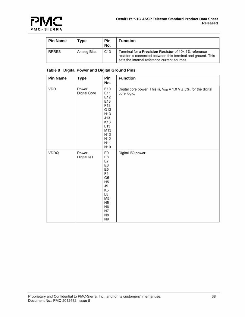
RPRES Analog Bias C13 Terminal for a Precision Resistor of 10k 1% reference resistor is connected between this terminal and ground. This sets the internal reference current sources.
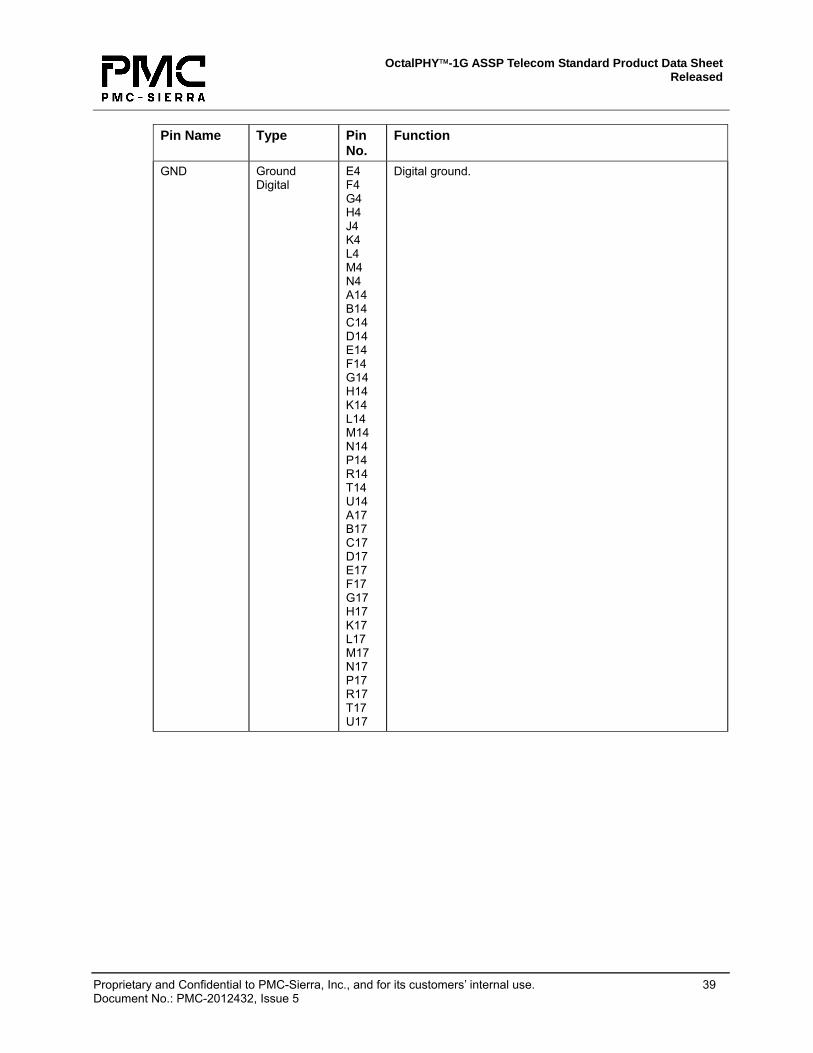
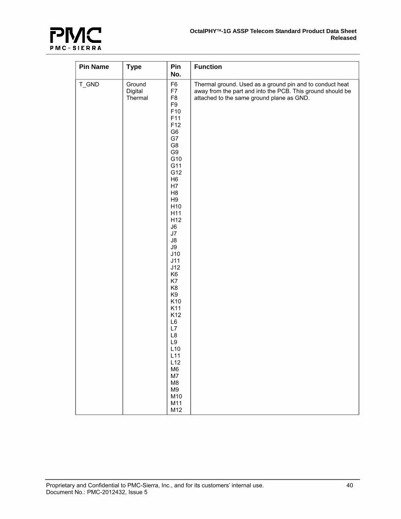
Thermal ground. Used as a ground pin and to conduct heat away from the part and into the PCB. This ground should be attached to the same ground plane as GND.
OctalPHY™-1G ASSP Telecom Standard Product Data Sheet Released
Proprietary and Confidential to PMC-Sierra, Inc., and for its customers’ internal use. 41 Document No.: PMC-2012432, Issue 5
Table 9 Analog Power and Ground Pins
Pin Name Type Pin No.
Function
VDDA Power Analog
J14 J15
Analog Power. This is, VDDA = 1.8 V ± 5% and must be separated from digital power.
GNDA Ground Analog
J16 J17
Analog ground. Connect to same ground plane as GND pins.
Notes:
1. All OctalPHY 1G inputs and bi-directionals present minimum capacitive loading and operate at CMOS logic levels.
2. Digital and analog ground pins are not connected together internally. Failure to connect any of these pins can cause malfunction or damage to the OctalPHY 1G.
3. Digital and analog power pins are not connected together internally. Failure to connect any of these pins could also result in malfunction or damage to the OctalPHY 1G.
OctalPHY™-1G ASSP Telecom Standard Product Data Sheet Released
Proprietary and Confidential to PMC-Sierra, Inc., and for its customers’ internal use. 42 Document No.: PMC-2012432, Issue 5
10 Functional Description
10.1 Modes of Operation
The OctalPHY 1G has four modes of operation:
1. Interleave Mode
2. Trunking Mode
3. Nibble Mode
4. Parallel Loopback Mode
Interleave, Trunking, and Parallel Loopback modes use the channel Receive FIFOs to synchronize the received data to the local clock domain (REFCLK). The Interleave and Trunking Modes configure the Parallel Receive and Transmit Interface into four 10-bit Interleaved Ports.
Nibble Mode bypasses the channel Receive FIFOs, which enables all eight channels to operate independently with their own recovered clock and data. Nibble Mode configures the Parallel Receive and Transmit Interface into eight 5-bit Independent Ports.
The 10-bit Interleave Mode is used whenever the Receive FIFO is enabled to synchronize the incoming serial data to the local clock domain determined by REFCLK. Interleave Mode multiplexes the eight serial channels into four 10-bit DDR parallel ports. Each port consists of a 10-bit receive data output bus and a 10-bit transmit data input bus. While operating in this mode, the OctalPHY 1G can be programmed to perform frequency compensation on a channel by channel basis, as well as trunking across all eight serial channels. Trunking allows the OctalPHY 1G to remove the skew (delay differences) between the 8 serial receive channels to enables the device to operate as a single 8 Gbit/s logical channel (when REFCLK = 125 MHz). The OctalPHY 1G can also be configured to perform Parallel Data Loopback while operating in the 10-bit Interleave Mode.
The 5-bit Nibble Mode is used whenever the Receive FIFO is bypassed. Nibble Mode redefines the four 10-bit ports that are used in Interleave Mode into eight 5-bit wide parallel interface ports. In this mode, all eight channels operate independently with their own recovered clock and data on a dedicated set of terminals. The transmit side still shares a clock on each pair of channels. Since this mode provides a recovered clock per channel, the frequency difference between REFCLK and recovered clock (receive data rate) is limited only by the capture range of the clock recovery circuit. The OctalPHY 1G clock recovery circuit can tolerate frequency differences of ±200 ppm of the REFCLK frequency (with no packet size or IPG restriction). This mode provides the lowest possible latency since the internal Receive FIFOs are bypassed.
OctalPHY™-1G ASSP Telecom Standard Product Data Sheet Released
Proprietary and Confidential to PMC-Sierra, Inc., and for its customers’ internal use. 43 Document No.: PMC-2012432, Issue 5
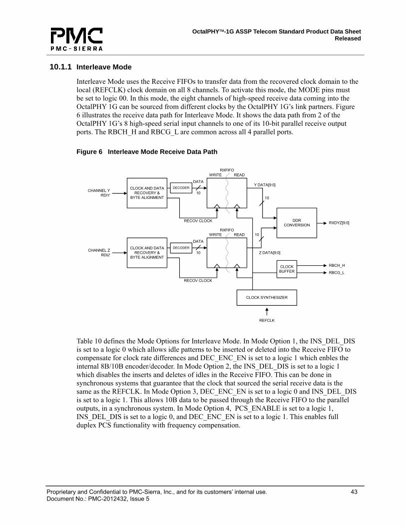
10.1.1 Interleave Mode
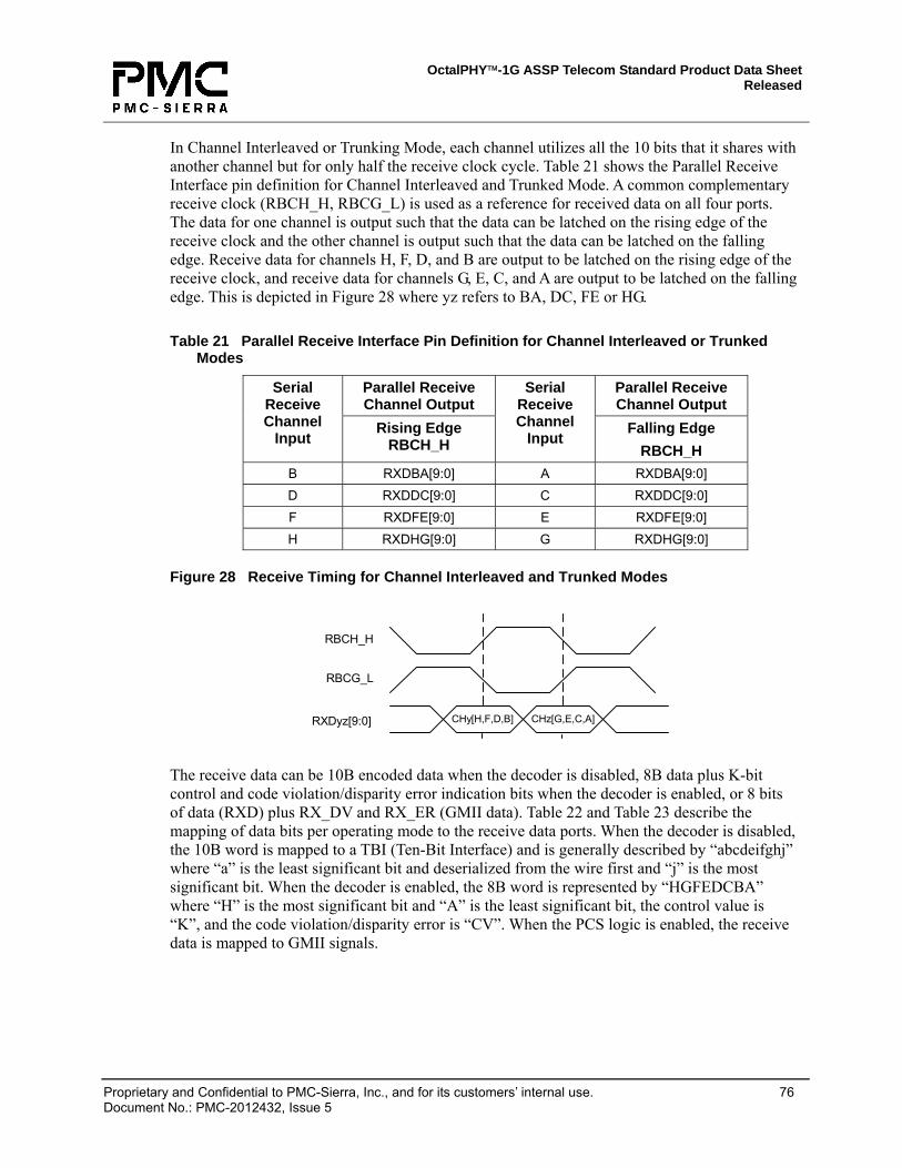
Interleave Mode uses the Receive FIFOs to transfer data from the recovered clock domain to the local (REFCLK) clock domain on all 8 channels. To activate this mode, the MODE pins must be set to logic 00. In this mode, the eight channels of high-speed receive data coming into the OctalPHY 1G can be sourced from different clocks by the OctalPHY 1G’s link partners. Figure 6 illustrates the receive data path for Interleave Mode. It shows the data path from 2 of the OctalPHY 1G’s 8 high-speed serial input channels to one of its 10-bit parallel receive output ports. The RBCH_H and RBCG_L are common across all 4 parallel ports.
Figure 6 Interleave Mode Receive Data Path
CLOCK AND DATARECOVERY &
BYTE ALIGNMENT
CLOCK AND DATARECOVERY &
BYTE ALIGNMENT
CHANNEL YRDIY
CHANNEL ZRDIZ
10
DATA
WRITE READRXFIFO
10
DATA
WRITE READRXFIFO
DDRCONVERSION
10
10
CLOCK SYNTHESIZER
REFCLK
RBCG_L
RXDYZ[9:0]RECOV CLOCK
Y DATA[9:0]
DECODER
DECODER
RECOV CLOCK
CLOCKBUFFER
RBCH_H
Z DATA[9:0]
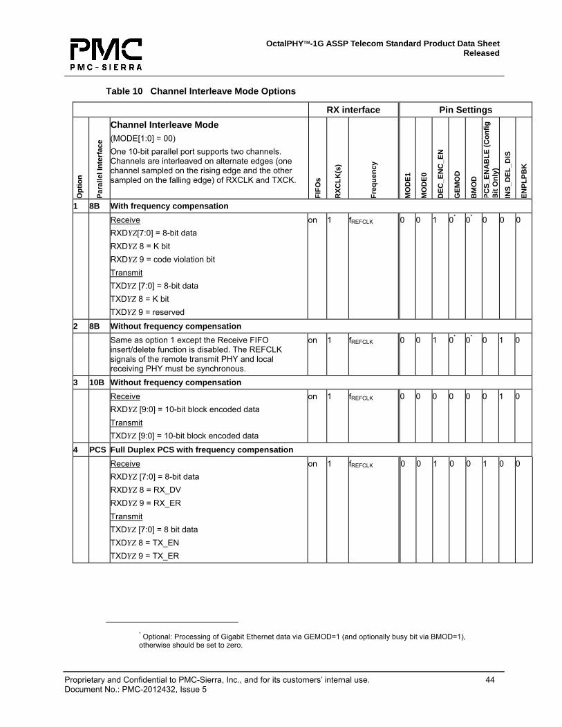
Table 10 defines the Mode Options for Interleave Mode. In Mode Option 1, the INS_DEL_DIS is set to a logic 0 which allows idle patterns to be inserted or deleted into the Receive FIFO to compensate for clock rate differences and DEC_ENC_EN is set to a logic 1 which enbles the internal 8B/10B encoder/decoder. In Mode Option 2, the INS_DEL_DIS is set to a logic 1 which disables the inserts and deletes of idles in the Receive FIFO. This can be done in synchronous systems that guarantee that the clock that sourced the serial receive data is the same as the REFCLK. In Mode Option 3, DEC_ENC_EN is set to a logic 0 and INS_DEL_DIS is set to a logic 1. This allows 10B data to be passed through the Receive FIFO to the parallel outputs, in a synchronous system. In Mode Option 4, PCS_ENABLE is set to a logic 1, INS_DEL_DIS is set to a logic 0, and DEC_ENC_EN is set to a logic 1. This enables full duplex PCS functionality with frequency compensation.
OctalPHY™-1G ASSP Telecom Standard Product Data Sheet Released
Proprietary and Confidential to PMC-Sierra, Inc., and for its customers’ internal use. 44 Document No.: PMC-2012432, Issue 5
Table 10 Channel Interleave Mode Options
RX interface Pin Settings
Opt
ion
Para
llel I
nter
face
Channel Interleave Mode (MODE[1:0] = 00) One 10-bit parallel port supports two channels. Channels are interleaved on alternate edges (one channel sampled on the rising edge and the other sampled on the falling edge) of RXCLK and TXCK. FI
FOs
RXC
LK(s
)
Freq
uenc
y
MO
DE1
MO
DE0
DEC
_EN
C_E
N
GEM
OD
BM
OD
PC
S_EN
AB
LE (C
onfig
B
it O
nly)
IN
S_D
EL_D
IS
ENPL
PBK
1 8B With frequency compensation Receive
RXDYZ[7:0] = 8-bit data RXDYZ 8 = K bit RXDYZ 9 = code violation bit Transmit TXDYZ [7:0] = 8-bit data TXDYZ 8 = K bit TXDYZ 9 = reserved
on 1 fREFCLK 0 0 1 0* 0* 0 0 0
2 8B Without frequency compensation Same as option 1 except the Receive FIFO
insert/delete function is disabled. The REFCLK signals of the remote transmit PHY and local receiving PHY must be synchronous.
on 1 fREFCLK 0 0 1 0* 0* 0 1 0
3 10B Without frequency compensation
Receive RXDYZ [9:0] = 10-bit block encoded data Transmit TXDYZ [9:0] = 10-bit block encoded data
on 1 fREFCLK 0 0 0 0 0 0 1 0
4 PCS Full Duplex PCS with frequency compensation Receive
RXDYZ [7:0] = 8-bit data RXDYZ 8 = RX_DV RXDYZ 9 = RX_ER Transmit TXDYZ [7:0] = 8 bit data TXDYZ 8 = TX_EN TXDYZ 9 = TX_ER
on 1 fREFCLK 0 0 1 0 0 1 0 0
* Optional: Processing of Gigabit Ethernet data via GEMOD=1 (and optionally busy bit via BMOD=1), otherwise should be set to zero.
OctalPHY™-1G ASSP Telecom Standard Product Data Sheet Released
Proprietary and Confidential to PMC-Sierra, Inc., and for its customers’ internal use. 45 Document No.: PMC-2012432, Issue 5
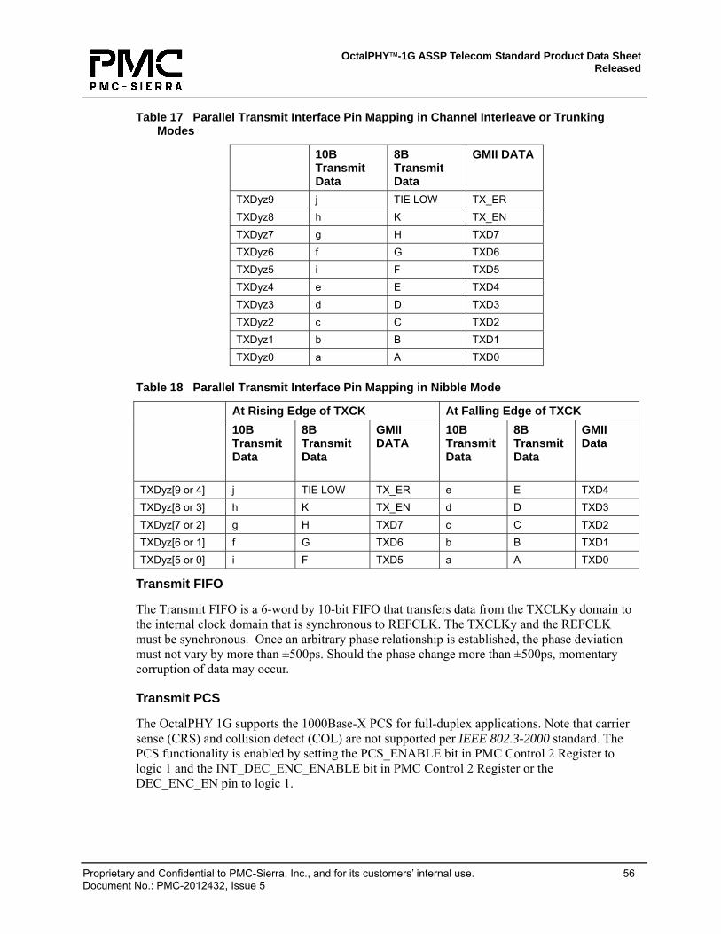
10.1.2 Trunking Mode
Trunking Mode operation is identical to Interleave Mode, except that it also compensates for differences in wire length between channels and allows the OctalPHY 1G to appear to operate as a single 8 Gbit/s logical channel (when REFCLK = 125 MHz). To activate this mode, the MODE pins must be set to logic 01. The Trunking process removes the skew (delay differences) between serial channels so that eight bytes transmitted together are aligned by the receiving device. This is achieved by sensing alignment information on each channel that identifies bytes to be aligned. All eight transmit channels are synchronous to each other and must be within ±200 ppm of the receive device’s REFCLK. Refer to the Receive FIFO description under section 10.2.4 Receive Path for a detailed explanation of the Trunking process.
This mode combines the eight serial streams into a single high bandwidth channel across eight channels in each direction. On the parallel side of the chip, the four ports are combined into forty bit wide, transmit and receive, DDR interfaces. A common complementary clock (RBCH_H, RBCG_L) is output as a reference for the received data. A common transmit clock, TXCKB, must be used to clock the TXDyz[9:0] input data when operating in Trunking Mode. TXCKB is used in this manner when the TXCLK4 bit in the PMC Control 2 Register is set to logic zero (default state). TXCKB must be synchronous to REFCLK in this mode.
The execution of a soft reset is recommended after the PLL has locked while operating in Trunking Mode.
It is possible to use fewer than 8 channels when operating in trunking mode, however the unused channels must be disabled through Register 0x10 (PMC Control Register 1).
Table 10 defines the Trunking Mode Options for Trunking Mode. Trunking Mode is not functional when the PCS logic is enabled, or when the GEMOD is set to a logic 1 or when DEC_ENC_EN is set to a logic 0. In Mode Option 1, the INS_DEL_DIS is set to a logic 0, which allows idle patterns to be inserted or deleted into the Receive FIFO to compensate for clock rate differences and. In Mode Option 2, the INS_DEL_DIS is set to a logic 1, which disables the inserts and deletes of idles in the Receive FIFO. This can only be done in synchronous systems that guarantee that the clock that sourced the serial receive data is the same as the REFCLK .
OctalPHY™-1G ASSP Telecom Standard Product Data Sheet Released
Proprietary and Confidential to PMC-Sierra, Inc., and for its customers’ internal use. 46 Document No.: PMC-2012432, Issue 5
Table 11 Trunking Mode Option
RX Interface Pin Settings
Opt
ion
Para
llel I
nter
face
Trunking Mode (MODE[1:0] = 01) Trunking aligns all eight channels to create a high bandwidth data channel. One 10-bit parallel port supports two channels. Channels are interleaved on alternate edges (one channel sampled on the rising edge and the other sampled on the falling edge) of RXCLK and TXCK. FI
FOs
RB
C(s
)
Freq
uenc
y
MO
DE1
MO
DE0
DEC
_EN
C_E
N
GEM
OD
BM
OD
PC
S_EN
AB
LE (C
onfig
B
it O
nly)
IN
S_D
EL_D
IS
ENPL
PBK
1 8B With frequency compensation
Receive RXDYZ [7:0] = 8-bit data RXDYZ 8 = K bit RXDYZ 9 = code violation bit Transmit TXDYZ [7:0] = 8-bit data TXDYZ 8 = K bit TXDYZ 9 = reserved
on 1 fREFCLK 0 1 1 0 0 0 0 0
2 8B Without frequency compensation
Receive RXDYZ [7:0] = 8-bit data RXDYZ 8 = K bit RXDYZ 9 = code violation bit Transmit TXDYZ [7:0] = 8-bit data TXDYZ 8 = K bit TXDYZ 9 = reserved
on 1 fREFCLK 0 1 1 0 0 0 1 0
OctalPHY™-1G ASSP Telecom Standard Product Data Sheet Released
Proprietary and Confidential to PMC-Sierra, Inc., and for its customers’ internal use. 47 Document No.: PMC-2012432, Issue 5
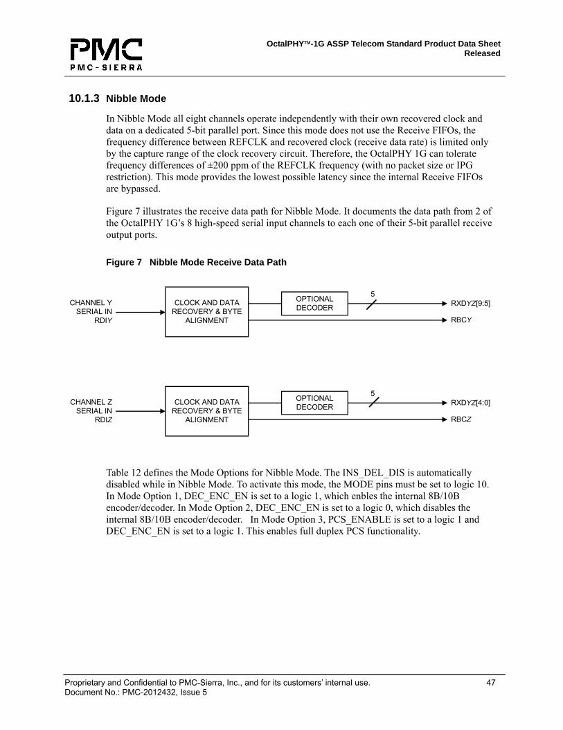
10.1.3 Nibble Mode
In Nibble Mode all eight channels operate independently with their own recovered clock and data on a dedicated 5-bit parallel port. Since this mode does not use the Receive FIFOs, the frequency difference between REFCLK and recovered clock (receive data rate) is limited only by the capture range of the clock recovery circuit. Therefore, the OctalPHY 1G can tolerate frequency differences of ±200 ppm of the REFCLK frequency (with no packet size or IPG restriction). This mode provides the lowest possible latency since the internal Receive FIFOs are bypassed.
Figure 7 illustrates the receive data path for Nibble Mode. It documents the data path from 2 of the OctalPHY 1G’s 8 high-speed serial input channels to each one of their 5-bit parallel receive output ports.
Figure 7 Nibble Mode Receive Data Path
CLOCK AND DATARECOVERY & BYTE
ALIGNMENT
CLOCK AND DATARECOVERY & BYTE
ALIGNMENT
5RXDYZ[9:5]
RXDYZ[4:0]
RBCZ
CHANNEL YSERIAL IN
RDIY
CHANNEL ZSERIAL IN
RDIZ
OPTIONALDECODER
OPTIONALDECODER
RBCY
5
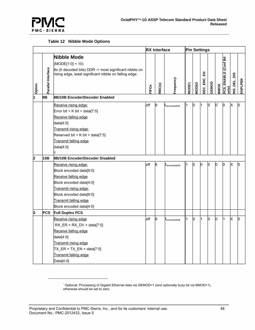
Table 12 defines the Mode Options for Nibble Mode. The INS_DEL_DIS is automatically disabled while in Nibble Mode. To activate this mode, the MODE pins must be set to logic 10. In Mode Option 1, DEC_ENC_EN is set to a logic 1, which enbles the internal 8B/10B encoder/decoder. In Mode Option 2, DEC_ENC_EN is set to a logic 0, which disables the internal 8B/10B encoder/decoder. In Mode Option 3, PCS_ENABLE is set to a logic 1 and DEC_ENC_EN is set to a logic 1. This enables full duplex PCS functionality.
OctalPHY™-1G ASSP Telecom Standard Product Data Sheet Released
Proprietary and Confidential to PMC-Sierra, Inc., and for its customers’ internal use. 48 Document No.: PMC-2012432, Issue 5
Table 12 Nibble Mode Options
RX interface Pin Settings
Opt
ion
Para
llel I
nter
face
Nibble Mode (MODE[1:0] = 10) 8x (5 decoded bits) DDR -> most significant nibble on rising edge, least significant nibble on falling edge. FI
* Optional: Processing of Gigabit Ethernet data via GEMOD=1 (and optionally busy bit via BMOD=1), otherwise should be set to zero.
OctalPHY™-1G ASSP Telecom Standard Product Data Sheet Released
Proprietary and Confidential to PMC-Sierra, Inc., and for its customers’ internal use. 49 Document No.: PMC-2012432, Issue 5
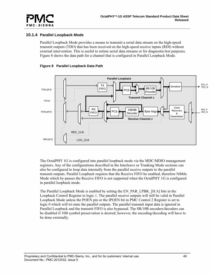
10.1.4 Parallel Loopback Mode
Parallel Loopback Mode provides a means to transmit a serial data stream on the high-speed transmit outputs (TDO) that has been received on the high-speed receive inputs (RDI) without external intervention. This is useful to retime serial data streams or for diagnostic/test purposes. Figure 8 shows the data path for a channel that is configured in Parallel Loopback Mode.
Figure 8 Parallel Loopback Data Path
TXFIFO
Transmit Channel z
SerializerPCS 8B/10B
Encoder
10B/8BDecoder Byte Align
ClockRecovery
&Deserializer
Receive Channel z
PCS
Parallel Loopback
TDO_P TDO_N
TXDyz[9:0]
TXCKz
LOC_CLK
REC_CLK
RXDyz[9:0]
RBCz[9:0]
RDI_P RDI_N
RXFIFO
The OctalPHY 1G is configured into parallel loopback mode via the MDC/MDIO management registers. Any of the configurations described in the Interleave or Trunking Mode sections can also be configured to loop data internally from the parallel receive outputs to the parallel transmit outputs. Parallel Loopback requires that the Receive FIFO be enabled, therefore Nibble Mode which by-passes the Receive FIFO is not supported when the OctalPHY 1G is configured in parallel loopback mode.
The Parallel Loopback Mode is enabled by setting the EN_PAR_LPBK_[H:A] bits in the Loopback Control Register to logic 1. The parallel receive outputs will still be valid in Parallel Loopback Mode unless the POEN pin or the IPOEN bit in PMC Control 2 Register is set to logic 0 which will tri-state the parallel outputs. The parallel transmit input data is ignored in Parallel Loopback and the transmit FIFO is also bypassed. The 8B/10B encoders/decoders can be disabled if 10B symbol preservation is desired; however, the encoding/decoding will have to be done externally.
OctalPHY™-1G ASSP Telecom Standard Product Data Sheet Released
Proprietary and Confidential to PMC-Sierra, Inc., and for its customers’ internal use. 50 Document No.: PMC-2012432, Issue 5
Table 13 Parallel Loopback Options
RX interface Pin Settings
Opt
ion
Para
llel I
nter
face
Parallel Loopback (ENPLBK = 1) FI
FOs
RB
C(s
)
Freq
uenc
y
MO
DE1
MO
DE0
DEC
_EN
C_E
N
GEM
OD
BM
OD
PC
S_EN
AB
LE (C
onf
Bit
only
) IN
S_D
EL_D
IS
ENPL
PBK
1 8B Local clock synchronization Receive data rate and local clock rate are different but
within ±200 ppm and packet lengths are < 214 bytes. Receive FIFO insert/delete logic is used to compensate for clock frequency differences *Optional: Processing of Gigabit Ethernet data via GEMOD = 1 (and optionally Busy Bit via BMOD = 1). Otherwise, should be set to 0.
on — fREFCLK 0 0 1 * * 0 0 1
2 8B Synchronous system
Receive data rate and local clock rate are the same. There is no limit on packet length. The encoder and decoder are enabled. Idle insert/delete is disabled. *Optional: Processing of Gigabit Ethernet data via GEMOD = 1 (and optionally Busy Bit via BMOD = 1). Otherwise, should be set to 0.
on — fREFCLK 0 0 1 * * 0 1 1
3 10B Synchronous system
Receive data rate and local clock rate are the same. There is no limit on packet length. The encoder and decoder are disabled. Idle insert/delete is disabled.
on — fREFCLK 0 0 0 0 0 0 1 1
4 8B Trunking
Trunking Mode is enabled. Receive FIFO insert/delete logic is used to compensate for clock frequency differences
on — fREFCLK 0 1 1 0 0 0 0 1
10.2 Serial Channel Overview
The OctalPHY 1G uses high-speed serial channel technology to communicate data between chips. Each channel consists of a differential transmit pair and a differential receive pair. The device supports PECL voltage swings and the receiver inputs are designed to be capacitively coupled external to the device. A clock is embedded in the serial data stream at the transmitter and extracted at the receiver, where it is used to recover the data. Data is de-serialized, decoded and processed internally as 9 bit bytes (8 data bits and 1 control bit) plus decode error indication. In Trunking Mode, up to 8 such groups of data are bound together into a single 64-bit wide data path supported by accompanying control signals.
OctalPHY™-1G ASSP Telecom Standard Product Data Sheet Released
Proprietary and Confidential to PMC-Sierra, Inc., and for its customers’ internal use. 51 Document No.: PMC-2012432, Issue 5
The OctalPHY 1G requires that received data to be 8B/10B encoded to ensure sufficient transition density. The OctalPHY 1G’s internal 8B/10B encoder/decoder can be disabled if an external 8B/10B encoder/decoder is used. The 8B/10B coding method offers several advantages including high-transition density, low DC offset and availability of special control characters (see Section 10.2.1).
10.2.1 8B Code Group Bit Mappings
All OctalPHY 1G registers that contain 8B code groups adhere to the following convention:
• Bit0, the LSB – contains the A-bit of the code group
• Bit7, the MSB – contains the H-bit of the code group
• Bit8, contains the k-bit (if applicable)
OctalPHY™-1G ASSP Telecom Standard Product Data Sheet Released
Proprietary and Confidential to PMC-Sierra, Inc., and for its customers’ internal use. 52 Document No.: PMC-2012432, Issue 5
Table 14 identifies the valid control code groups that will encode/decode properly. Do not specify any other control code groups in the OctalPHY 1G registers or apply these code groups to the TXDxy[8:0] interface.
Table 14 Valid K Bit Values
K-Bit Valid 9-bit Value (hex) Code Definition K28.0 0x11C /R/1 Suggested Skip/Replace Idle Character K28.1 0x13C Alternate Skip/Replace Idle Character K28.2 0x15C Alternate Skip/Replace Idle Character K28.3 0x17C /A/ Suggested Alignment Idle Character K28.4 0x19C Alternate Skip/Replace Idle Character K28.5 0x1BC /K/ Synchronization Idle Character K28.6 0x1DC Alternate Skip/Replace Idle Character K28.7 0x1FC Special Diagnostics Character K23.7 0x1F7 /R/ Carrier-Extend for 1000BaseX PCS Apps K27.7 0x1FB /S/ Start-of-Packet K29.7 0x1FD /T/ End-of-Packet K30.7 0x1FE /V/ Error Propagation
Note:
1. Refer to Table 48-4 Defined ordered_sets and special code groups in the IEEE Draft P802.3-2000.
For backplane applications, the usage of these characters is not limited by the OctalPHY 1G. Any characters not used as Alignment or Idle characters will be passed transparently between OctalPHY 1G devices.
For Gigabit Ethernet applications, these characters must be used in a manner consistent with the 802.3 specification.
10.2.2 Clock Synthesizer
The Clock Synthesizer uses a PLL to synthesize a clock from the REFCLK input. The frequency of the PLL clock is 10 times the frequency of REFCLK, and a single synthesized clock is used to transmit serial data on all 8 transmit channels.
The PLL clock frequency can be varied over a range of 1.0 GHz to 1.25 GHz by changing the frequency of REFCLK. The PLL has a fixed multiplication ratio of 10, so the frequency of REFCLK must be 1/10 the required PLL clock frequency as illustrated in Table 15.
The PLL in the Clock Synthesizer requires a 10 k Ω ± 1% precision resistor on the RPRES terminal.
OctalPHY™-1G ASSP Telecom Standard Product Data Sheet Released
Proprietary and Confidential to PMC-Sierra, Inc., and for its customers’ internal use. 53 Document No.: PMC-2012432, Issue 5
Table 15 Example REFCLK and PLL Clock Combinations
REFCLK Frequency
Multiplier PLL Clock Frequency
Transmit Data Rate
93.3 MHz 10x 933MHz 933 Mbit/s
106.25 MHz 10X 1.0625 GHz 1.0625 Gbit/s
125 MHz 10X 1.25 GHz 1.25 Gbit/s
10.2.3 Transmit Path
The OctalPHY 1G contains eight transmit channels. Each channel consists of a DDR Parallel Interface, Transmit FIFO, Transmit PCS, 8B/10B Encoder, and Serializer. The configuration of these functional blocks is shown in Figure 9.
The device can accept 8-bit plus control bit, GMII formatted data, or 10-bit coded data on the TXDyz ports. The data must be frequency synchronous with REFCLK. The 8B/10B encoder and PCS logic may be bypassed depending on the type of data presented.
Figure 9 Transmit Channel Functional Blocks
TxFIFO SerializerPCS 8B/10B
Encoder
Transmit Channel
TDO_PTDO_NTXDyz[9:0]
TXCKy
ParallelLoopbackData Path
DDRInterface
DDR Parallel Interface
The transmit parallel interface consists of 40 pins that are shared across 8 transmit channels. Channels A and B share 10 pins, as do channels C and D, E and F, and G and H. The pins are shared by applying the input data in a Dual-Data Rate (DDR) fashion, that is, data is applied on the rising and falling edges of the transmit clock. There are two modes of DDR for this interface: Nibble Mode and Interleaved/Trunking Mode.
OctalPHY™-1G ASSP Telecom Standard Product Data Sheet Released
Proprietary and Confidential to PMC-Sierra, Inc., and for its customers’ internal use. 54 Document No.: PMC-2012432, Issue 5
Table 16 shows the mapping during Nibble Mode operation of the 4 parallel transmit input ports to the 8 high-speed serial transmit output channels.
Table 16 Parallel Transmit Interface Pin Definition for Nibble Mode
Parallel Transmit
Input Ports
Transmit Reference
Clock
Data Loaded
Serial Transmit Output
Channel Rising Edge Falling Edge
TXDBA[4:0] TXCKB TXDA[9:5] TXDA[4:0] A TXDBA[5:9] TXCKB TXDB[9:5] TXDB[4:0] B TXDDC[4:0] TXCKD TXDC[9:5] TXDC[4:0] C TXDDC[5:9] TXCKD TXDD[9:5] TXDD[4:0] D TXDFE[4:0] TXCKF TXDE[9:5] TXDE[4:0] E TXDFE[5:9] TXCKF TXDF[9:5] TXDF[4:0] F TXDHG[4:0] TXCKH TXDG[9:5] TXDG[4:0] G TXDHG[5:9] TXCKH TXDH[9:5] TXDH[4:0] H
In Nibble mode, the most significant 5 bits of data are applied relative to the positive edge and the least significant 5 bits are applied relative to the negative edge of the corresponding transmit clock. Figure 10 depicts the transmit timing for Nibble Mode; where yz refers to BA, DC, FE or HG.
Figure 10 Transmit Timing for Nibble Mode
TXCKy
TXDyz[9:5]
TXDyz[4:0]
TXDy[4:0]TXDy[9:5]
TXDz[9:5] TXDz[4:0]
In Channel Interleaved or Trunking Mode, each channel utilizes all 10 bits that it shares with another channel but for only half the transmit clock cycle. The data for one channel is sampled on the rising edge and the other channel is sampled on the falling edge of the corresponding transmit clock. Transmit data for channels H, F, D, and B are sampled on the rising edge of the corresponding transmit clock, and transmit data for channels G, E, C, and A are sampled on the falling edge. This is depicted in Figure 11, where yz refers to BA, DC, FE or HG.
OctalPHY™-1G ASSP Telecom Standard Product Data Sheet Released
Proprietary and Confidential to PMC-Sierra, Inc., and for its customers’ internal use. 55 Document No.: PMC-2012432, Issue 5
Figure 11 Transmit Timing for Channel Interleave Mode
TXCKy
TXDyz[9:0] CHy[H,F,D,B] CHz[G,E,C,A]
The device may be configured where each TXDyz port has it’s own clock or where all four share a common clock while in Interleave or Nibble modes.
When the TXCLK4 bit in PMC Control 2 Register is set to logic 0, all of the TXDyz ports are sampled by a common clock, TXCKB.
When the TXCLK4 bit is set to logic 1, TXCKB samples TXDBA, TXCKD samples TXDDC, TXCKF samples TXDFE and TXCKH samples TXDHG. Clocks TXCKB, TXCKD, TXCKF, and TXCKH must all be synchronous to REFCLK, but the phase of each clock can be different. The Transmit FIFO will account for the phase differences. The transmit data can be 10B encoded data if the encoder is disabled, 8B data plus K control bit if the encoder is enabled, or 8 bits of data (TXD) plus TX_EN and TX_ER for Gigabit Ethernet applications
Figure 12 Transmit Timing for Trunking Mode
TXCKB
TXDyz[9:0] CHy[H,F,D,B] CHz[G,E,C,A]
While operating in Trunking mode, one common clock, TXCKB, must be used to clock all 4 TXDyz[9:0] input busses. This requires that the TXCLK4 bit be set to logic 0. Table 17 and Table 18 describe the mapping of data bits per operating mode to the transmit data ports. When the encoder is disabled, the 10B word is mapped to a TBI (Ten-Bit Interface) and is generally described by “abcdeifghj” where “a” is the least significant bit and serialized onto the wire first and “j” is the most significant bit. When the encoder is enabled, the 8B word is represented by “HGFEDCBA” where “H” is the most significant bit and “A” is the least significant bit, and the control value is “K”. When the PCS logic is enabled, the transmit data is mapped to GMII signals. When the encoder is enabled, the transmit data is 10B encoded internally and is generally described by “abcdeifghj” where “a” is the least significant bit and serialized onto the wire first and “j” is the most significant bit.
OctalPHY™-1G ASSP Telecom Standard Product Data Sheet Released
Proprietary and Confidential to PMC-Sierra, Inc., and for its customers’ internal use. 56 Document No.: PMC-2012432, Issue 5
Table 17 Parallel Transmit Interface Pin Mapping in Channel Interleave or Trunking Modes
10B Transmit Data
8B Transmit Data
GMII DATA
TXDyz9 j TIE LOW TX_ER TXDyz8 h K TX_EN TXDyz7 g H TXD7 TXDyz6 f G TXD6 TXDyz5 i F TXD5 TXDyz4 e E TXD4 TXDyz3 d D TXD3 TXDyz2 c C TXD2 TXDyz1 b B TXD1 TXDyz0 a A TXD0
Table 18 Parallel Transmit Interface Pin Mapping in Nibble Mode
At Rising Edge of TXCK At Falling Edge of TXCK
10B Transmit Data
8B Transmit Data
GMII DATA
10B Transmit Data
8B Transmit Data
GMII Data
TXDyz[9 or 4] j TIE LOW TX_ER e E TXD4 TXDyz[8 or 3] h K TX_EN d D TXD3 TXDyz[7 or 2] g H TXD7 c C TXD2 TXDyz[6 or 1] f G TXD6 b B TXD1 TXDyz[5 or 0] i F TXD5 a A TXD0
Transmit FIFO
The Transmit FIFO is a 6-word by 10-bit FIFO that transfers data from the TXCLKy domain to the internal clock domain that is synchronous to REFCLK. The TXCLKy and the REFCLK must be synchronous. Once an arbitrary phase relationship is established, the phase deviation must not vary by more than ±500ps. Should the phase change more than ±500ps, momentary corruption of data may occur.
Transmit PCS
The OctalPHY 1G supports the 1000Base-X PCS for full-duplex applications. Note that carrier sense (CRS) and collision detect (COL) are not supported per IEEE 802.3-2000 standard. The PCS functionality is enabled by setting the PCS_ENABLE bit in PMC Control 2 Register to logic 1 and the INT_DEC_ENC_ENABLE bit in PMC Control 2 Register or the DEC_ENC_EN pin to logic 1.
OctalPHY™-1G ASSP Telecom Standard Product Data Sheet Released
Proprietary and Confidential to PMC-Sierra, Inc., and for its customers’ internal use. 57 Document No.: PMC-2012432, Issue 5
The PCS transmit logic contains an 8B/10B encoder and a single transmit state machine whose operation is consistent with the operation of the two transmit state machines that run in unison within clause 36 of IEEE 802.3-2000. All transmit blocks are compliant with the IEEE 802.3-2000 (Clauses 36 and 37).
OctalPHY™-1G ASSP Telecom Standard Product Data Sheet Released
Proprietary and Confidential to PMC-Sierra, Inc., and for its customers’ internal use. 58 Document No.: PMC-2012432, Issue 5
From IEEE Std. 802.3-2000 [1] Copyright 2000 IEEE. All rights reserved.*
OctalPHY™-1G ASSP Telecom Standard Product Data Sheet Released
Proprietary and Confidential to PMC-Sierra, Inc., and for its customers’ internal use. 59 Document No.: PMC-2012432, Issue 5
8B/10B Encoder
When enabled, the encoder accepts an 8-bit word plus the k-bit and encodes these bits into a 10-bit parallel code. The encoder generates a running disparity for its own use in generating sub-blocks of 6- and 4-bit codes that limit the run length and maintain DC balance of the serialized bits. The user can present data as an un-encoded byte along with a control signal indicating a "K" character, or can disable the encoding logic and present pre-encoded 10-bit data. The Encoder logic is enabled either by connecting the DEC_ENC_EN pin to logic 1 or programming PMC Control 2 Register, bit 7 (INT_DEC_ENC_ENABLE) with logic value 1. Rules for encoding are specified in IEEE 802.3-2000.
When the encoder is enabled and input pin GEMOD or PMC Control 3 Register, bit 15 (GE_REG) is set to logic 1 and PMC Control 2 Register, bit 2 (PCS_ENABLE) is set to logic 0, the encoder will substitute a D5.6 octet for a D16.2 octet when it follows a K28.5 character and the current running disparity is negative. This functionality is useful when the input data stream is generated from a 1000Base-X PCS Transmit state machine and the current running disparity during Interpacket Gap (IPG) must be maintained such that positive commas are encoded.
In Trunking Mode, the encoder can also substitute an alignment character, the octet value programmed into the A_CHAR bits in the Trunking Control Register, for the second octet of an idle sequence [idle sequences are defined in registers 0x12 and 0x13, and 0x14 and 0x15] when the INSERT_A_CHAR register bit in the Trunking Control register is set to logic 1. All channels being trunked must currently be transmitting the same idle sequence for the second half of the idle to be replaced. Idles will be replaced by the A_CHAR register value at a frequency determined by the A_DELAY bits in the Trunking Control register.
Serializer
The serializer accepts 10-bit transmission characters and converts them from a parallel format to a serial bit stream at bit rates between 933 Mbit/s Gbit/s and 1.25 Gbit/s. The serializer accepts a 10-bit parallel word with the least significant bit being transmitted first.
10.2.4 Receive Path
The OctalPHY 1G contains eight receive channels. Each channel consists of a Clock and Data Recovery Unit (CDRU), Byte Alignment logic, 8/B/10B Decoder, Receive PCS, Receive FIFO, and a DDR Parallel Output Interface. The configuration of these functional blocks are shown in Figure 15.
OctalPHY™-1G ASSP Telecom Standard Product Data Sheet Released
Proprietary and Confidential to PMC-Sierra, Inc., and for its customers’ internal use. 60 Document No.: PMC-2012432, Issue 5
Figure 15 Receive Channel Functional Blocks
10B/8BDecoder Byte Align
Receive Channel A
FIFO PCS
LOC_CLK
RXDyz[9:0] RDI_P RDI_N
REC_CLKRBCz
SerialLoopbackData Path
ClockRecovery
&Deserializer
DDRInterface
Each channel’s CDRU, comma detection and byte alignment logic run independently. The comma detection logic is programmable to detect +comma, -comma, or both. The decoded words with K bits are optionally retimed by the Receive FIFO with IDLE character insertion/deletion for frequency compensation. The eight channels are also optionally column aligned to /A/, alignment character as programmed into the Trunking Control register, or idle to data transitions across the eight channels.
The receiver input data must be AC coupled with a transfer rate between 933 Mbit/s and 1.25 Gbit/s. The OctalPHY 1G supports on-chip 100Ω differential termination. The data is expected to be a 10-bit encoded data stream as specified in IEEE 802.3-2000. The clock recovery circuit recovers a clock (REC_CLK) from the incoming data. The recovered clock is used to sample the data. Both the recovered clock and data are provided to the deserializer independently for each channel.
Serial input ports may be internally looped-back to the serial output ports for testing purposes. While in a serial loopback mode, the serial output pins are held at a differential one. Serial loopback may be enabled using one of the following mechanisms:
• Assert IENSLPBKn control bit in the Loopback Control Register
• Assert Loopback bit in the channel’s GMII Control register
• Assert EN_SLPBK pin to loopback all channels simultaneously
When the CODE_VIOL_DIS_ENABLE (bit 14 PMC Control 2) bit is set or the CV_DIS_EN pin is asserted, a code or disparity violation detected by the receiver will replace the byte in violation by the encoding of all 1’s or 0xFF on the data pins and a 1 on the K bit and the associated code error counter is incremented. The error code is propagated through OctalPHY 1G and eventually transmitted at the egress.
OctalPHY™-1G ASSP Telecom Standard Product Data Sheet Released
Proprietary and Confidential to PMC-Sierra, Inc., and for its customers’ internal use. 61 Document No.: PMC-2012432, Issue 5
Clock and Data Recovery
A 933 Mbit/s to 1.25 Gbit/s receive clock is extracted from the 10-bit coded serial data stream independently on each channel. The data rate of the received serial bit stream should be between 933 Mbit/s and 1.25 Gbit/s to guarantee proper lock. The receive clock locks to the input within 2 µS after a valid input data stream is applied. The received data is de-serialized and byte aligned. The recovered clock will be synchronous to the REFCLK if no data is present on the RDI serial inputs. The de-serializer converts the received serial stream into 10-bit parallel data.
The bit synchronization time, the time required for the Clock and Data Recovery unit to recover the incoming bitstream error-free, is influenced by several factors including:
o Receive jitter. o Relative phase difference between the incoming bitstream and the signal to which the
CDRU was previously synchronized. o Transition density. o DC Common Mode voltage offsets
The bit synchronization time is independent of the ppm offset, but the incoming bitstream must be within +/- 200 ppm of the local REFCLK.
The maximum bit synchronization time is required under conditions of minimum permissible receiver eye opening & worst-case relative phase difference alignment between the bitstream and the CDR. Under these conditions, the maximum bit sync time is determined by the transition density of the incoming bit stream. Should a difference in DC Common Mode voltages exist, the minimum signal amplitude must be increased by an equivalent amount in order to maintain the shortest possible bit sync time.
An 8B/10B coded bitstreams that contain the idle ordered set of K28.5, D16.2 will provide a nominal transition density of approximately 60%, and will result in a maximum bit synchronization time of 500 bit times With other transition densities, the bit synchronization time can be calculated as:
T_BitSync (in bit times) = 24000 / nominal transition density (expressed as a percentage)
This determination of bit sync time is only applicable when the CDRU inputs are switched from one transitioning bitstream to another. Should the inputs remain inactive for several 1000s of bit times, bit synchronization will be delayed while the external AC coupling capacitors at the input of the SERDES charge to their steady state values. In this case, the maximum bit synchronization time is 2000 bit times.
OctalPHY™-1G ASSP Telecom Standard Product Data Sheet Released
Proprietary and Confidential to PMC-Sierra, Inc., and for its customers’ internal use. 62 Document No.: PMC-2012432, Issue 5
Byte Alignment and Synchronization
The character alignment logic searches the coded incoming serial stream for a sequence defined in IEEE 802.3-2000 as a comma. A comma is the sequence 0011111 or its complement and is unique in valid 10B coded data. This makes the comma useful for detecting proper alignment of incoming characters to byte boundaries. Upon detection of a comma, the alignment logic shifts the incoming data to align the received data properly in the 10-bit character field. An optional Byte-Sync State machine, shown in Figure 16, is implemented on a per channel basis to enable character alignment and preserve the alignment through occasional bit errors.
If a channel’s Byte Synchronization State Machine is in the LOSS_OF_SYNC state, it can acquire synchronization by detecting four code-groups that contain commas without detecting code-group errors. An initial comma must be detected by the character alignment logic before the state machine can start the synchronization process. Once synchronization is acquired, the channel moves into the SYNC_ACQ_1 state. The state machine tests the received code-group to move between the SYNC_ACQ_1 and LOSS_OF_SYNC states. To prevent loss of synchronization during occasional bit errors, hysteresis can be added by setting the BA_HYST_EN bit in PMC Control 3 Register. The Byte Sync State Machine operates independently from the PCS Synchronization State Machine described in PCS Receive Section.
Hysteresis is normally disabled upon reset. In this case, once the channel’s synchronization state machine has entered the SYNC_ACQ_1 state, any realignment caused by the detection of a comma in a new location causes the channel to move to the LOSS_OF_SYNC state. If hysteresis is enabled, the synchronization process uses the hysteresis defined in the synchronization state machine. Even if a channel’s hysteresis is disabled, the synchronization state machine continues to monitor alignment and supply a synchronization status indication. If a channel’s synchronization state machine enters the LOSS_OF_SYNC state, the corresponding BYTE_ALIGN_STAT_[D:A] bit in Auto-Negotiation Status Register 2 latches the low valued status and holds it until a read of that register is performed.
The serial bit stream must be ordered ‘abcdeifghj’ with ‘a’ being the first bit received and ‘j’ the last bit received. The recovered receive clocks are neither stretched nor slivered during character alignment. During alignment up to, but not exceeding, four 10-bit code groups may be deleted or modified while aligning the code group to the edges of the receive clock.
OctalPHY™-1G ASSP Telecom Standard Product Data Sheet Released
Proprietary and Confidential to PMC-Sierra, Inc., and for its customers’ internal use. 63 Document No.: PMC-2012432, Issue 5
Figure 16 Byte Synchronization State Machine
LOSS_OF_SYNCbyte_align_stat=0
en_cdet=1
SYNC_ACQ_3good_cgs=0
SYNC_ACQ_2Agood_cgs=good_cgs+1
COM_DET_3
SYNC_ACQ_2good_cgs=0
SYNC_ACQ_3Agood_cgs=good_cgs+1
SYNC_ACQ_4good_cgs=0
SYNC_ACQ_4Agood_cgs=good_cgs+1
COM_DET_2
COM_DET_1en_cdet=0
2
1
1
2
reset = 0
bs!=comma(comma = K28.5 or K28.1
or K28.7)
bs = invalid
bs_invalid
bs=comma
bs=valid & bs!=comma
bs=valid & bs!=comma
bs=valid & bs!=comma
bs=comma
bs=comma
Note:1. bs = Byte Synchronized Data2. When in the LOSS_OF_SYNC state,an additional comma is required by thebyte alignment logic to synhronize to thenew byte boundary.
bs_invalid
bs=invalid
bs=invalid bs=invalid
bs=invalid bs=invalid
bs=invalidbs=invalid
bs=valid
bs=valid
bs=valid
bs=valid &good_cgs=3
bs=valid & good_cgs=3
bs=valid & good_cgs=3
bs=valid &good_cgs!=3
bs=valid &good_cgs!=3
bs=valid &good_cgs!=3
bs=valid
SYNC_ACQ_1byte_align_stat=1
bs=comma
OctalPHY™-1G ASSP Telecom Standard Product Data Sheet Released
Proprietary and Confidential to PMC-Sierra, Inc., and for its customers’ internal use. 64 Document No.: PMC-2012432, Issue 5
8B/10B Decoder
When enabled, each receive channel decodes incoming data into an 8-bit data byte and an associated control bit called the k-bit. Information is routed and processed internally in this 9-bit parallel form. The decoder monitors for proper disparity and coding logging errors. A 10th bit for indicating a code violation or disparity error is also routed with the 9-bit parallel data. When the CODE_VIOL_DIS_ENABLE (bit 14 PMC Control 2) or the CV_DIS_EN pin is set, errors are reinforced by the receiver by substituting the code, 0x3FF, for the byte in error.
When the EN_CODE_ERR_CHK bit in Register 0x1B is a logic 1, the 8B/10B decoder in the corresponding channel will count coding errors received and will flag the error count reaching the maximum set by PKT_CNT[14:0] in Register 0x1C. The error will be indicated by the CODE_ERR_EXCEED bit in register 0x1B being read as logic 1. CODE_ERR_EXCEED will hold the error until register 0x1B is read. The 8B/10B coding error counters in all channels will be cleared whenever the CODE_ERR_STB bit in register 0x18 is set to logic 1. CODE_ERR_STB is self-clearing.
Receive PCS
The OctalPHY 1G supports the 1000Base-X PCS for full-duplex applications. Note that carrier sense (CRS) and collision detect (COL) are not supported per IEEE 802.3-2000 standard. The PCS functionality is enabled by setting the PCS_ENABLE bit and the INT_DEC_ENC_ENABLE bit in Register 0x11.
The PCS receive logic contains an 8B/10B decoder, synchronization state machine, carrier detection logic, receive state machine, and auto-negotiation (AN) state machine. All receive blocks are compliant with the IEEE 802.3-2000 (Clauses 36 and 37). The PCS Synchronization State Machine is shown in Figures 17 –19. The PCS Auto-negotiation State Machine, shown in Figure 20, supports both base page and next page exchange as well as having programmable link timers. The link timer value can be programmed via LINK_TIMER_MODE bits [1:0] of Register 0x11. The link timers can be set to approximately 12.6 ms or 16.8 ms to be compliant with the IEEE 802.3-2000, the default is 16.8 ms. These state machines are enabled when the PCS_ENABLE bit in Register 0x11 is set to a logic 1.
The management interface provides AN registers as prescribed by IEEE 802.3-2000. Additionally, two status registers, Registers 0x19 (Auto Negotiation Status 1) and 0x1A (Auto Negotiation Status 2), have been added for polling the eight separate ports with a single management register read. Register 0x19 contains a base page received and a next page received indication for each port. These bits clear on read. Normally during AN, a channel's base page received bit will get set once and then the next page received bit for that channel would get set for any subsequent pages received. If the base page received bit becomes set again during AN, it is an indication that AN has been restarted for that port. Register 0x1A contains an indication for each channel that AN has completed. Both of the status registers reflect same information found in Register 0x01 (Status), bit 5 and Register 0x06 (AN Expansion), bit 1. Reading Register 0x19 only clears that register; it does not clear the page received bits in Register 0x06. The opposite is also true; when reading Register 0x06, Register 0x19 is not cleared.
Additional information on PCS and GMII can be found in IEEE 802.3 sections 35 and 36.
OctalPHY™-1G ASSP Telecom Standard Product Data Sheet Released
Proprietary and Confidential to PMC-Sierra, Inc., and for its customers’ internal use. 65 Document No.: PMC-2012432, Issue 5
OctalPHY™-1G ASSP Telecom Standard Product Data Sheet Released
Proprietary and Confidential to PMC-Sierra, Inc., and for its customers’ internal use. 66 Document No.: PMC-2012432, Issue 5
Receive FIFO
The Receive FIFO transfers data from the recovered clock domain to the internal clock domain that is synchronous to REFCLK. The Receive FIFO compensates for differences in the clock tolerances. The Receive FIFO is used in the channel Interleaved/Trunking Mode. The Receive FIFO is not used in Nibble Mode. In addition, in Trunking Mode, the Receive FIFO is used for channel (lane) alignment, removing skew differences between channels.
The Receive FIFO achieves clock tolerance compensation by inserting or deleting 2 octet wide IDLE sequences as needed. Figure 21 illustrates the insertion (and deletion) of an IDLE sequence when the recovered clock is running slower (or faster) than the REFCLK. The Receive FIFO will only delete an IDLE sequence when more than one IDLE sequences has been recognized. When the Receive FIFO inserts an IDLE sequence, the IDLE sequence inserted is the same as the previous IDLE sequence received.
Figure 21 Insertion/Deletion of Idle Sequences by the Receive FIFO
D I2I1D... DD ...DDI2I1 I2I1
2-byte IdleSequences
D I2I1D... DD ...DDI2I1 DD
Data Stream Input into the Receive FIFO
D I2I1D... I2I1 ...DDI2I1 I2I1
Idle sequence inserted
Data Stream After Idle Sequence Deleted bythe Receive FIFO
Data Stream After Idle Sequence Inserted bythe Receive FIFO
The IDLE sequences are defined by registers 0x12 through 0x15. Registers 0x12 – 0x15 are only used by the Receive FIFO and will not affect the de-serialization process. These registers are formatted as K-bit (bit 8) and data (bits 7:0). Generally, IDLE1 and IDLE1A should be programmed to one of the three valid control characters (K28.1, K28.5, or K28.7) that contain a comma pattern. The decoder must be enabled for the Receive FIFO to use these register values in the clock tolerance compensation logic.
OctalPHY™-1G ASSP Telecom Standard Product Data Sheet Released
Proprietary and Confidential to PMC-Sierra, Inc., and for its customers’ internal use. 67 Document No.: PMC-2012432, Issue 5
The alternate IDLE sequence registers, IDLE1A and IDLE2A, are available for applications that make use of multiple idle sequences to indicate system conditions. An example of this would be flow control. One IDLE sequence might indicate clear to send while the other sequence indicated not clear to send. If only one IDLE sequence is desired, the two pairs of control registers should be programmed to the same values.
The OctalPHY 1G uses the values stored in the IDLE sequence registers to insert or delete idles in the Receive FIFO. Data can be presented to the OctalPHY 1G with either an IDLE1 or IDLE1A that is not followed by an IDLE2 or IDLE2A. In this condition, the data that follows the IDLE1 or IDLE1A must not be the same as the data stored in the IDLE2 or IDLE2A registers. If the data is the same, the OctalPHY 1G decodes the data pattern that follows the IDLE1 or IDLE1A as a valid IDLE2 or IDLE2A character and could delete it.
Even if the incoming data stream does not contain IDLE sequences, the Receive FIFO can still transfer data from the recovered clock domain to the REFCLK domain and compensate for phase only. The insertion and deletion of IDLE sequences for clock tolerance compensation can be disabled by setting the INS_DEL_DIS bit in PMC Control 3 Register to logic 1.
The depth of the Receive FIFO determines the amount of clock frequency difference the OctalPHY 1G can tolerate. The OctalPHY 1G has a sixteen (16) character deep FIFO on each receive channel. This enables the OctalPHY 1G to tolerate up to ±200 ppm clock differences on 1600 byte packets with 4 byte IPG. However, larger packet sizes (16K bytes) can be accommodated in systems with tighter clock differences (±100 ppm) and appropriate IPG (4 bytes).
The typical additional latency due to FIFO operation is six bytes. To accommodate 16K-byte packets with ±100 ppm reference clock difference between systems, the alignment logic requires that it be able to insert or remove two IDLE sequences between packets. Depending on the relative frequency between REFCLK and the received data frequency, the additional latency due to the FIFO operation could be 2 bytes to 12 bytes.
In Trunking Mode, the Receive FIFO realigns the read pointers to remove channel-to-channel skew differences in addition to performing clock tolerance compensation. Trunking Mode is not functional when the PCS logic is enabled, or when the GEMOD pin or GE_REG bit is set to logic 1. There are two methods of alignment based on the A_CHAR_EN bit in the Trunking Control Register. When A_CHAR_EN is set to logic 1, the Trunking logic within the Receive FIFO looks for an alignment character in each channel being trunked and then realigns all trunked channels’ read pointers to the address of the alignment character. The alignment character is defined in the Trunking Control Register. If the INSERT_A_CHAR bit within the Trunking Control Register is set to logic 1, then the Receive FIFO replaces all alignment characters with either an IDLE2 or IDLE2A character depending on the preceding byte being an IDLE1 or IDLE1A, respectively. Figure 22 illustrates Trunking with A_CHAR_EN set to logic 1 and INSERT_A_CHAR set to logic 0.
OctalPHY™-1G ASSP Telecom Standard Product Data Sheet Released
Proprietary and Confidential to PMC-Sierra, Inc., and for its customers’ internal use. 68 Document No.: PMC-2012432, Issue 5
Figure 22 Trunking Mode Channel Alignment using Alignment Characters
A I1 I2I1I2I1I2 ...DDD I1DD I1I2I1AI1 A I1 I2I1I2I1I2 ...DDD I1DD I2I1A
I1 A I1 I2I1I2I1I2 ...DDD I1DDI1 I2 I1AI1 A I1 I2I1I2I1I2 ...DDD I1DD I1I2I1A
I2I2
Data Containing Alignment Characters Received with Skew
Data Aligned Utilizing Alignment Characters
I1 A I1 I2I1I2I1I2 ...DDD I1DDI1 I2 I1AI1 A I1 I2I1I2I1I2 ...DDD I1DD I1I2I1A
I1 A I1 I2I1I2I1I2 ...DDD I1DD I2I1AI2
A I1 I2I1I2I1I2 ...DDD I1DD I1I2I1A I2
I1 A I1 I2I1I2I1I2 ...DDD I1DD I1I2I1AI1 A I1 I2I1I2I1I2 ...DDD I1DD I1I2I1AI1 A I1 I2I1I2I1I2 ...DDD I1DD I1I2I1AI1 A I1 I2I1I2I1I2 ...DDD I1DD I1I2I1A
I1 A I1 I2I1I2I1I2 ...DDD I1DD I1I2I1AI1 A I1 I2I1I2I1I2 ...DDD I1DD I1I2I1AI1 A I1 I2I1I2I1I2 ...DDD I1DD I1I2I1AI1 A I1 I2I1I2I1I2 ...DDD I1DD I1I2I1A
Channel A
Channel H
Channel A
Channel H
If the INSERT_A_CHAR bit is set to logic 0 and the A_CHAR_EN bit is set to logic 1, then it is assumed that the alignment character, as defined in the Trunking Control Register, will be present in the Inter Packet Gap periodically inserted into the data stream, across all channels simultaneously.
The alignment character should be present in the received data periodically to induce continuous alignment of all channels. Two or more alignment characters may be present during an IPG, but they must be separated by a distance that is greater than or equal to 16 bytes which is the depth of the receive FIFO.
When A_CHAR_EN is set to logic 0, the Trunking logic within the Receive FIFO looks for a transition from IDLE sequences to data (or non-IDLE sequences). All channels being trunked will realign their read pointers to the transition from IDLE sequence to data simultaneously. Figure 23 illustrates Trunking with A_CHAR_EN set to logic 0.
OctalPHY™-1G ASSP Telecom Standard Product Data Sheet Released
Proprietary and Confidential to PMC-Sierra, Inc., and for its customers’ internal use. 69 Document No.: PMC-2012432, Issue 5
While operating in the idle-data transition mode, frames should not be sent more often then every 16 columns or 128 bytes (including the IPG). This guarantees that there is enough separation between transitions so that a false realignment will not occur. If packets are required to be sent closer together, it is recommended that the deskew state machines be enabled to reduce the risk of a false channel realignment.
Figure 23 Trunking Mode Channel Alignment using the Transition from Idle to Data
Data Not Containing Alignment Characters Received with Skew
When Trunking, the Receive FIFO performs clock tolerance compensation across all trunked channels simultaneously. All channels must possess valid IDLE sequences for an insertion or deletion of a column of IDLE sequences to occur. Figure 24 illustrates an insertion of a column of IDLE sequences when Trunking. Figure 25 illustrates an deletion of a column of IDLE sequences when Trunking.
OctalPHY™-1G ASSP Telecom Standard Product Data Sheet Released
Proprietary and Confidential to PMC-Sierra, Inc., and for its customers’ internal use. 70 Document No.: PMC-2012432, Issue 5
The OctalPHY 1G can be used to trunk less than 8 channels at a time, but the unused OctalPHY channels must be disabled. Those channels that are disabled will have no bearing on the alignment or clock tolerance compensation operations.
Figure 24 Insertion of a Column of Idle Sequences when Trunking
D I2I1D...
D I2I1D...D I2I1D...D I2I1D...
DD ...DD
DD ...DDDD ...DDDD ...DD
I2I1
I2I1I2I1I2I1
I2I1
I2I1I2I1I2I1
2-Byte IdleSequences
D I2DD...
D I2I1D...D I2I1D...D I2I1D...
DD ...DD
DD ...DDDD ...DDDD ...DD
I2I1
I2I1I2I1I2I1
I2I1
I2I1I2I1I2I1
I2I1
I2I1I2I1I2I1
Trunked Aligned Data Stream
Idle Sequence Inserted
D I2DD...
D I2I1D...D I2I1D...D I2I1D...
DD ...DD
DD ...DDDD ...DDDD ...DD
I2I1
I2I1I2I1I2I1
I2I1
I2I1I2I1I2I1
Channel A
Channel H
D I2I1D...
D I2I1D...D I2I1D...D I2I1D...
DD ...DD
DD ...DDDD ...DDDD ...DD
I2I1
I2I1I2I1I2I1
I2I1
I2I1I2I1I2I1
I2I1
I2I1I2I1I2I1
Channel A
Channel H
OctalPHY™-1G ASSP Telecom Standard Product Data Sheet Released
Proprietary and Confidential to PMC-Sierra, Inc., and for its customers’ internal use. 71 Document No.: PMC-2012432, Issue 5
Figure 25 Deletion of a Column of Idle Sequences when Trunking
D I2I1D...
D I2I1D...D I2I1D...D I2I1D...
DD ...DD
DD ...DDDD ...DDDD ...DD
I2I1
I2I1I2I1I2I1
I2I1
I2I1I2I1I2I1
2-Byte IdleSequences
Trunked Aligned Data Stream
Idle Sequence Deleted
D I2DD...
D I2I1D...D I2I1D...D I2I1D...
DD ...DD
DD ...DDDD ...DDDD ...DD
I2I1
I2I1I2I1I2I1
I2I1
I2I1I2I1I2I1
D I2TD...
D I2I1D...D I2I1D...D I2I1D...
DS ...DD
DD ...DDDD ...DDDD ...DD
I2I1
I2I1I2I1I2I1
D I2DD...
D I2I1D...D I2I1D...D I2I1D...
DD ...DD
DD ...DDDD ...DDDD ...DD
I2I1
I2I1I2I1I2I1
Channel A
Channel H
Channel A
Channel H
OctalPHY™-1G ASSP Telecom Standard Product Data Sheet Released
Proprietary and Confidential to PMC-Sierra, Inc., and for its customers’ internal use. 72 Document No.: PMC-2012432, Issue 5
Maximum Size Packets Supported
Internal logic within the OctalPHY 1G establishes a relationship between the frequency at which serial data is received (fDATA) and ten times the reference clock frequency (fREFCLK) provided by the local clock. This relationship allows the device to recover incoming serial data and place it on the REFCLK domain for further processing. The difference in these two frequencies is usually stated in parts per million (ppm) and is calculated as follows:
Clock compensation is the ability for the OctalPHY 1G to adjust for this frequency difference. It uses internal FIFOs to accomplish this.
These same FIFOs are used to eliminate the skew between lanes when in trunking mode. Lane skew is defined as the difference in time between the most delayed lane to the least delayed lane. For convenience, lane skew is measured in bits (b). The absolute delay on any one lane is not relevant in device performance except for its contribution to overall latency.
The size of these internal FIFOs mathematically establish the maximum packet size supported by the device given b and cppm on a per lane basis. Another factor in determining maximum packet size is whether or not the DESKEW_HYST_EN is enabled (see register 0x18: PMC Control 3). If this register (D) is set to a zero, further maximum packet size degradation occurs.
Equation 2 below is a conservative closed form solution of the largest packet size (Smax) supported by the OctalPHY 1G as a function of the number of bits of skew, whether DESKEW_HYST_EN is asserted, the number of lanes (n) being used and the difference is clock frequency in ppm.
Smax = 106 • (5 + D - int[(b+11)/10]) • n / cppm (2)
As long as the system is operating synchronously (cppm = 0) and the skew between lanes is less than 40, there is no maximum packet size. Note that for calculations in which the part is not in trunking mode, the skew (b) should be zero and the lanes (n) should be 1. Table 19 gives some examples of maximum packet sizes that are typical in a system.
Table 19 Maximum Packet Size Supported
Smax (bytes) b (bits) D (unitless) n (lanes) cppm (unitless)
OctalPHY™-1G ASSP Telecom Standard Product Data Sheet Released
Proprietary and Confidential to PMC-Sierra, Inc., and for its customers’ internal use. 73 Document No.: PMC-2012432, Issue 5
10.2.5 Trunking Logic
The trunking logic determines when all lanes being trunked will realign, insert an idle column or delete an idle column when in trunking mode. A two octet wide idle column will be inserted or deleted if all lanes being trunked contain the same idle pattern and at least one lane needs to have an idle inserted or deleted to compensate for the clock rate differences. The trunking logic contains a deskew state machine that monitors the lane to lane word alignment. The deskew state machine determines with hysteresis if all lanes are aligned. The alignment status is reported via the DESKEW_STATUS bit in the Trunking Control register. The deskew state machine is shown in Figure 26.
Figure 26 Deskew State Machine
Loss ofAlignment
AlignmentDetect 1
AlignmentDetect 3
AlignmentDetect 2
AlignmentAcquired 3
AlignmentAcquired 2
AlignmentError Wait
AlignmentAcquired 1
AlignmentError Wait 2
1
1
A
B
C
C
C
B
B
B
Condition A : Received data or unaligned A characters.Condition B: Received correctly aligned A characters.Condition C: Received data, not unaligned A characters.Condition D: Received unaligned A characters.Condition E: Received data or aligned A characters.
D
D
D
D
D
E
C
C
C
B
B
B
D
Reset or loss of sync
OctalPHY™-1G ASSP Telecom Standard Product Data Sheet Released
Proprietary and Confidential to PMC-Sierra, Inc., and for its customers’ internal use. 74 Document No.: PMC-2012432, Issue 5
All lanes will realign when an alignment character, as defined in the Trunking Control register, is found in each lane’s receive FIFO. When DESKEW_HYST_EN in the PMC Control register 3 is a logic 0, realignment will occur whenever there are alignment characters in all receive FIFOs. If all lanes are currently word aligned, a realignment will have no affect on the output data or the receive FIFOs’ pointers. When DESKEW_HYST_EN is logic 1, the deskew state machine will control when realignment can occur; realignment will only occur when the deskew state machine is in the Loss of Alignment state.
A subset of the eight lanes provided by OctalPHY 1G can be trunked by disabling the undesired channels’ ENABLE_CHN_[H:A] bits in PMC Control Register 1.
10.2.6 Gigabit Ethernet and PCS Operating Modes
PCS_ENABLE (bit 2 in Register 0x11h) is used to enable the 1000Base-X PCS logic. The GEMOD pin or the GE_REG register bit is used to enable a small subset of “PCS-type” functions. The description below specifies the exact functions that the GEMOD/GE_REG affects.
Note that PCS_ENABLE should not be set to logic 1 when either GEMOD or GE_REG register is set to logic 1.
Gigabit Ethernet with PCS Enabled
When the PCS logic is enabled the parallel interface is formatted as GMII data. The PCS logic includes TX and RX state machines, auto-negotiation and byte alignment logic that are fully compliant with the IEEE 802.3 1000Base-X PCS specification.
Gigabit Ethernet with PCS Disabled - GEMOD Enabled and BMOD Disabled
When the GEMOD pin or GE_REG bit in the PMC Control 3 Register is set to logic 1, the parallel interface is formatted as 8B data. The receive FIFO recognizes a decoded /K28.5/ pattern followed by any valid data pattern, /Dx.y/, excluding the /D21.5/ and /D2.2/ data patterns, as an IDLE sequence that can be used for insertion or deletion in clock tolerance compensation. A decoded /K28.5/ pattern followed by the /D21.5/ or /D2.2/ data patterns and then followed by 2 valid data bytes are recognized as a 4-byte configuration pattern as sent during auto-negotiation. These 4-byte configuration patterns can be inserted or deleted for clock tolerance compensation.
Also, in this mode of operation IDLE patterns are corrected to ensure negative running disparity during the IPG by substituting /D5.6/ for /D16.2/ in a /K28.5/Dx.y/ transmit IDLE pair.
Note that Auto-Negotiation functions are NOT performed when GEMOD=1.
Gigabit Ethernet with PCS Disabled - GEMOD Enabled and BMOD Enabled
This mode operates the same as Gigabit Ethernet with PCS Disabled - GEMOD enabled and BMOD disabled shown above. For this mode, when the BMOD pin or the BUSY_REG bit in the PMC Control 3 Register is set to logic 1, a decoded /K28.5/ pattern followed by a /D10.1/ data byte will not be recognized as an IDLE sequence and will not be inserted or deleted.
OctalPHY™-1G ASSP Telecom Standard Product Data Sheet Released
Proprietary and Confidential to PMC-Sierra, Inc., and for its customers’ internal use. 75 Document No.: PMC-2012432, Issue 5
10.2.7 DDR Parallel Outputs
The parallel receive interface consists of 40 pins that are shared across 8 channels. Channels A and B share 10 pins, as do channels C and D, E and F, and G and H. The pins are shared by applying the input data in a Dual-Data Rate (DDR) fashion, that is, data is output on each edge of the receive clock. There are two modes of DDR for this interface. In Nibble Mode, the parallel receive interface is partitioned into 8 5-bit ports. Each channel has a dedicated 5-bit port. Table 20 shows the Parallel Receive Interface Pin Definition for Nibble Mode. The upper 5 bits of a channel’s data are output relative to the positive edge of the corresponding receive clock and the lower 5 bits are output relative to the negative edge of the receive clock. Figure 27 shown the transmit timing for Nibble Mode; where yz refers to BA, DC, FE or HG.
Table 20 Parallel Receive Interface Pin Definition for Nibble Mode
Parallel Receive Channel Output
Reference Clock
Data Available
Serial Receive Channel
Input Rising Edge Falling Edge
A RXDBA[4:0] RBCA RXDA[9:5] RXDA[4:0] B RXDBA[5:9] RBCB RXDB[9:5] RXDB[4:0] C RXDDC[4:0] RBCC RXDC[9:5] RXDC[4:0] D RXDDC[5:9] RBCD RXDD[9:5] RXDD[4:0] E RXDFE[4:0] RBCE RXDE[9:5] RXDE[4:0] F RXDFE[5:9] RBCF RXDF[9:5] RXDF[4:0] G RXDHG[4:0] RBCG_L RXDG[9:5] RXDG[4:0] H RXDHG[5:9] RBCH_H RXDH[9:5] RXDH[4:0]
Figure 27 Receive Timing for Nibble Mode
RBCy
RXDy[9:5] RXDy[4:0]RXDyz[9:5]
RBCz
RXDz[9:5] RXDz[4:0]RXDyz[4:0]
OctalPHY™-1G ASSP Telecom Standard Product Data Sheet Released
Proprietary and Confidential to PMC-Sierra, Inc., and for its customers’ internal use. 76 Document No.: PMC-2012432, Issue 5
In Channel Interleaved or Trunking Mode, each channel utilizes all the 10 bits that it shares with another channel but for only half the receive clock cycle. Table 21 shows the Parallel Receive Interface pin definition for Channel Interleaved and Trunked Mode. A common complementary receive clock (RBCH_H, RBCG_L) is used as a reference for received data on all four ports. The data for one channel is output such that the data can be latched on the rising edge of the receive clock and the other channel is output such that the data can be latched on the falling edge. Receive data for channels H, F, D, and B are output to be latched on the rising edge of the receive clock, and receive data for channels G, E, C, and A are output to be latched on the falling edge. This is depicted in Figure 28 where yz refers to BA, DC, FE or HG.
Table 21 Parallel Receive Interface Pin Definition for Channel Interleaved or Trunked Modes
Parallel Receive Channel Output
Parallel Receive Channel Output
Serial Receive Channel
Input Rising Edge
RBCH_H
Serial Receive Channel
Input Falling Edge
RBCH_H
B RXDBA[9:0] A RXDBA[9:0] D RXDDC[9:0] C RXDDC[9:0] F RXDFE[9:0] E RXDFE[9:0] H RXDHG[9:0] G RXDHG[9:0]
Figure 28 Receive Timing for Channel Interleaved and Trunked Modes
RBCH_H
RBCG_L
RXDyz[9:0] CHy[H,F,D,B] CHz[G,E,C,A]
The receive data can be 10B encoded data when the decoder is disabled, 8B data plus K-bit control and code violation/disparity error indication bits when the decoder is enabled, or 8 bits of data (RXD) plus RX_DV and RX_ER (GMII data). Table 22 and Table 23 describe the mapping of data bits per operating mode to the receive data ports. When the decoder is disabled, the 10B word is mapped to a TBI (Ten-Bit Interface) and is generally described by “abcdeifghj” where “a” is the least significant bit and deserialized from the wire first and “j” is the most significant bit. When the decoder is enabled, the 8B word is represented by “HGFEDCBA” where “H” is the most significant bit and “A” is the least significant bit, the control value is “K”, and the code violation/disparity error is “CV”. When the PCS logic is enabled, the receive data is mapped to GMII signals.
OctalPHY™-1G ASSP Telecom Standard Product Data Sheet Released
Proprietary and Confidential to PMC-Sierra, Inc., and for its customers’ internal use. 77 Document No.: PMC-2012432, Issue 5
Table 22 Parallel Receive Interface Pin Mapping in Channel Interleaved or Trunked Mode
10B Receive Data
8B Receive Data
GMII DATA
RXDyz9 J CV RX_ER RXDyz8 H K RX_DV RXDyz7 G H RXD7 RXDyz6 F G RXD6 RXDyz5 I F RXD5 RXDyz4 E E RXD4 RXDyz3 D D RXD3 RXDyz2 C C RXD2 RXDyz1 B B RXD1 RXDyz0 A A RXD0
Table 23 Parallel Receive Interface Pin Mapping in Nibble Mode
10.3 JTAG Test Access Port
The OctalPHY 1G supports the IEEE Boundary Scan Specification as described in the IEEE 1149.1 standards. The JTAG Test Access Port (TAP) consists of the five standard pins, TRSTB, TCK, TMS, TDI and TDO used to control the TAP controller and the boundary scan registers. The TRSTB input is the active-low reset signal used to reset the TAP controller. TCK is the test clock used to sample data on input, TDI and to output data on output, TDO. The TMS input is used to direct the TAP controller through its states. The basic boundary scan architecture is shown below.
At Rising Edge of RBCH_H At Falling Edge of RBCH_H 10B
Receive Data
8B Receive Data
GMII DATA
10B Receive Data
8B Receive Data
GMII Data
RXDyz[9 or 4] j CV RX_ER e E RXD4 RXDyz[8 or 3] h K RX_DV d D RXD3 RXDyz[7 or 2] g H RXD7 c C RXD2 RXDyz[6 or 1] f G RXD6 b B RXD1 RXDyz[5 or 0] i F RXD5 a A RXD0
OctalPHY™-1G ASSP Telecom Standard Product Data Sheet Released
Proprietary and Confidential to PMC-Sierra, Inc., and for its customers’ internal use. 78 Document No.: PMC-2012432, Issue 5
Figure 29 Boundary Scan Architecture
Boundary Scan Register
Control
TDI
TDO
Device Identification Register
Bypass Register
Instruction Register
and Decode
TRSTB
TMS
TCK
Test Access
Port Controller
Mux DFF
Select
Tri-state Enable
The boundary scan architecture consists of a TAP controller, an instruction register with instruction decode, a bypass register, a device identification register and a boundary scan register. The TAP controller interprets the TMS input and generates control signals to load the instruction and data registers. The instruction register with instruction decode block is used to select the test to be executed and/or the register to be accessed. The bypass register offers a single-bit delay from primary input, TDI to primary output, TDO. The device identification register contains the device identification code.
The boundary scan register allows testing of board inter-connectivity. The boundary scan register consists of a shift register place in series with device inputs and outputs. Using the boundary scan register, all digital inputs can be sampled and shifted out on primary output, TDO. In addition, patterns can be shifted in on primary input, TDI and forced onto all digital outputs.
10.3.1 TAP Controller
The TAP controller is a synchronous finite state machine clocked by the rising edge of primary input, TCK. All state transitions are controlled using primary input, TMS. The finite state machine is shown in Figure 30.
OctalPHY™-1G ASSP Telecom Standard Product Data Sheet Released
Proprietary and Confidential to PMC-Sierra, Inc., and for its customers’ internal use. 79 Document No.: PMC-2012432, Issue 5
Figure 30 TAP Controller Finite State Machine
Test-Logic-Reset
Run-Test-Idle Select-DR-Scan Select-IR-Scan
Capture-DR Capture-IR
Shift-DR Shift-IR
Exit1-DR Exit1-IR
Pause-DR Pause-IR
Exit2-DR Exit2-IR
Update-DR Update-IR
TRSTB=0
0
0
0
0
0
0
1 11
1
1
1
1
1
1
0
0
0
0
0
1
1
1
1
1
1
0
0
0
0
0
1
Notes:
1. TRSTB must be set to a logic 1 in order to transition out of the Test-Logic-Reset State.
OctalPHY™-1G ASSP Telecom Standard Product Data Sheet Released
Proprietary and Confidential to PMC-Sierra, Inc., and for its customers’ internal use. 80 Document No.: PMC-2012432, Issue 5
2. The value shown adjacent to each state transition in Figure 30 represents the signal present at TMS at the rising edge of TCK.
3. All transitions are dependent on the logic level of TMS.
Test-Logic-Reset
The test logic reset state is used to disable the TAP logic when the device is in normal mode operation. The state is entered asynchronously by asserting input, TRSTB. The state is entered synchronously regardless of the current TAP controller state by forcing input, TMS high for 5 TCK clock cycles. While in this state, the instruction register is set to the IDCODE instruction.
Run-Test-Idle
The run test/idle state is used to execute tests.
Capture-DR
The capture data register state is used to load parallel data into the test data registers selected by the current instruction. If the selected register does not allow parallel loads or no loading is required by the current instruction, the test register maintains its value. Loading occurs on the rising edge of TCK.
Shift-DR
The shift data register state is used to shift the selected test data registers by one stage. Shifting is from MSB to LSB and occurs on the rising edge of TCK.
Update-DR
The update data register state is used to load a test register's parallel output latch. In general, the output latches are used to control the device. For example, for the EXTEST instruction, the boundary scan test register's parallel output latches are used to control the device's outputs. The parallel output latches are updated on the falling edge of TCK.
Capture-IR
The capture instruction register state is used to load the instruction register with a fixed instruction. The load occurs on the rising edge of TCK.
Shift-IR
The shift instruction register state is used to shift both the instruction register and the selected test data registers by one stage. Shifting is from MSB to LSB and occurs on the rising edge of TCK.
Update-IR
The update instruction register state is used to load a new instruction into the instruction register. The new instruction must be scanned in using the Shift-IR state. The load occurs on the falling edge of TCK.
OctalPHY™-1G ASSP Telecom Standard Product Data Sheet Released
Proprietary and Confidential to PMC-Sierra, Inc., and for its customers’ internal use. 81 Document No.: PMC-2012432, Issue 5
The Pause-DR and Pause-IR states are provided to allow shifting through the test data and/or instruction registers to be momentarily paused.
10.3.2 Boundary Scan Instructions
The following is an description of the standard instructions. Each instruction selects a serial test data register path between input, TDI and output, TDO.
BYPASS
The bypass instruction shifts data from input, TDI to output, TDO with one TCK clock period delay. The instruction is used to bypass the device.
EXTEST
The external test instruction allows testing of the interconnection to other devices. When the current instruction is the EXTEST instruction, the boundary scan register is placed between input, TDI and output, TDO. Primary device inputs can be sampled by loading the boundary scan register using the Capture-DR state. The sampled values can then be viewed by shifting the boundary scan register using the Shift-DR state. Primary device outputs can be controlled by loading patterns shifted in through input TDI into the boundary scan register using the Update-DR state.
SAMPLE
The sample instruction samples all the device inputs and outputs. For this instruction, the boundary scan register is placed between TDI and TDO. Primary device inputs and outputs can be sampled by loading the boundary scan register using the Capture-DR state. The sampled values can then be viewed by shifting the boundary scan register using the Shift-DR state.
IDCODE
The identification instruction is used to connect the identification register between TDI and TDO. The device's identification code can then be shifted out using the Shift-DR state. The OctalPHY 1G identification code has not been assigned at this time.
STCTEST
The single transport chain instruction is used to test out the TAP controller and the boundary scan register during production test. When this instruction is the current instruction, the boundary scan register is connected between TDI and TDO. During the Capture-DR state, the device identification code is loaded into the boundary scan register. The code can then be shifted out output, TDO using the Shift-DR state
OctalPHY™-1G ASSP Telecom Standard Product Data Sheet Released
Proprietary and Confidential to PMC-Sierra, Inc., and for its customers’ internal use. 82 Document No.: PMC-2012432, Issue 5
10.4 Microprocessor Interface
The OctalPHY 1G implements a management interface that uses a protocol defined in IEEE 802.3. This 2-wire interface is used for configuration, control and status of up to four OctalPHY 1G devices and consists of MDC (management data clock) and MDIO (management data I/O) terminals. This interface allows serial read/write of internal control and status registers. The register map is defined in Figure 33. Note that there are both global address registers, a single register used for all channels and addressed only by bits PHYAD[4:3] of the management frame, and per-port addressed registers, a register addressed using all bits of PHYAD of the management frame. Figure 31 illustrates the addressing of both the global and per-port registers.
OctalPHY™-1G ASSP Telecom Standard Product Data Sheet Released
Proprietary and Confidential to PMC-Sierra, Inc., and for its customers’ internal use. 83 Document No.: PMC-2012432, Issue 5
PRE (Preamble) - At the beginning of each transaction, the management interface controller sends a sequence of 32 contiguous logic 1 bits on MDIO with 32 corresponding cycles on MDC to provide the OctalPHY 1G with a pattern that it can use to establish synchronization. The OctalPHY 1G observes a sequence of 32 contiguous 1 bits on MDIO with 32 corresponding cycles on MDC before it responds to any transaction.
ST (Start of Frame) - is indicated by a <01> pattern. This pattern assures transitions from the default logic 1 line state to 0 and back to 1.
OP (Operation Code) - The operation code for a read transaction is <10>, while the operation code for a write transaction is <01>.
PHYAD (PHY Address) - is 5 bits, allowing 32 unique device addresses (i.e., four OctalPHY 1Gs consisting of eight devices each.) The first PHY address bit transmitted and received is the MSB of the address.
The OctalPHY 1G will respond only when the PHYAD[4:3] bits match the DVAD[4:3] terminal values. A given port is addressable by the PHYAD[2:0] bits. Note the DVAD[2:0] terminals are unused and should be tied to ground.
REGAD (Register Address) – is 5 bits, allowing 32 individual registers to be addressed within each OctalPHY 1G. The first Register Address bit transmitted and received is the MSB of the address.
TA (Turnaround) – is a 2-bit time spacing between the Register Address field and the Data field of a management frame to avoid contention during a read transaction. For a read transaction, both the management interface controller and the OctalPHY 1G remain in a high-impedance state for the first bit time of the turnaround. The OctalPHY 1G drives a 0 bit during the second bit time of the turnaround of a read transaction. During a write transaction, the management interface controller drives a 1 bit for the first bit time of the turnaround and a 0 bit for the second bit time of the turnaround.
OctalPHY™-1G ASSP Telecom Standard Product Data Sheet Released
Proprietary and Confidential to PMC-Sierra, Inc., and for its customers’ internal use. 85 Document No.: PMC-2012432, Issue 5
Figure 32 Behavior of MDIO During TA Field of a Read Transaction
MDC
MDIO
<R> <Z> <0>
DATA - 16-bit field. The first data bit transmitted and received is bit 15 (MSB) of the register being addressed.
IDLE – logic state on MDIO is high-impedance. MDIO must be pulled high when not driven.
Figure 33 Register Memory Map
Address (Hex)
Register
0x00 GMII Control 0x01 GMII Status 0x02 GMII PHY Identifier 0x03 GMII PHY Identifier 0x04 GMII Auto-Negotiation Advertisement 0x05 GMII Auto-Negotiation Link Partner Base Page Ability 0x06 GMII Auto-Negotiation Expansion 0x07 GMII Auto-Negotiation Next Page Transmit 0x08 GMII Auto-Negotiation Link Partner Next Page Received 0x09 GMII Reserved 0x0A GMII Reserved 0x0B GMII Reserved 0x0C GMII Reserved 0x0D GMII Reserved 0x0E GMII Reserved 0x0F GMII Extended Status 0x10 PMC Control 1 0x11 PMC Control 2 0x12 IDLE 1 0x13 IDLE 2 0x14 IDLE 1A 0x15 IDLE 2A 0x16 Loopback Control
OctalPHY™-1G ASSP Telecom Standard Product Data Sheet Released
Proprietary and Confidential to PMC-Sierra, Inc., and for its customers’ internal use. 86 Document No.: PMC-2012432, Issue 5
Address (Hex)
Register
0x17 Trunking Control 0x18 PMC Control 3 0x19 Auto-Negotiation Status 1 0x1A Auto-Negotiation Status 2 0x1B Packet Generator/Checker Control/Status 0x1C Packet Generator Count Control 0x1D PMC Reserved 0x1E Reserved/PMC Test 1 0x1F Reserved/PMC Test 2
Note:
1. Registers 0x00 – 0x0F are only valid when PCS_ENABLE = 1.
2. Registers 0x1B and 0x1C are only valid when PCS_ENBABLE = 0.
OctalPHY™-1G ASSP Telecom Standard Product Data Sheet Released
Proprietary and Confidential to PMC-Sierra, Inc., and for its customers’ internal use. 87 Document No.: PMC-2012432, Issue 5
11 Normal Mode Register Description Normal mode registers are used to configure and monitor the operation of the OctalPHY 1G.
Notes on Normal Mode Register Bits:
1. Writing values into unused register bits has no effect. However, to ensure software compatibility with future, feature-enhanced versions of the product, unused register bits must be written with logic zero. Reading back unused bits can produce either a logic one or a logic zero; hence, unused register bits should be masked off by software when read
2. In configuration bits that can be written into can also be read back. This allows the processor controlling the OctalPHY 1G to determine the programming state of the block
3. Writeable normal mode register bits are cleared to logic zero upon reset unless otherwise noted
4. Writing into read-only normal mode register bit locations does not affect OctalPHY 1G operation unless otherwise noted
5. Certain register bits are reserved. These bits are associated with either reserved addresses dictated by the IEEE 802.3 standard or PMC-Sierra Test functions. To ensure that the OctalPHY 1G operates as intended, reserved register bits must be written with their default value as indicated by the register bit description
11.1 IEEE Defined Registers
Register 0x00: GMII Control
Bit Type Function Default Bit 15 R/W1 RESET 0 Bit 14 R/W LOOPBACK 0 Bit 13 R SPEED_SELECTION_LSB 0 Bit 12 R/W AN_ENABLE 1 Bit 11 R/W POWER_DOWN 0 Bit 10 R/W ISOLATE 0 Bit 9 R/W1 RESTART_AN 0 Bit 8 R DUPLEX_MODE 1 Bit 7 R COLLISION_TEST 0 Bit 6 R SPEED_SELECTION_MSB 1 Bit 5 R RESERVED 0 Bit 4 R RESERVED 0 Bit 3 R RESERVED 0 Bit 2 R RESERVED 0 Bit 1 R RESERVED 0 Bit 0 R RESERVED 0
Notes:
1. When written with a 1, this bit self clears.
The GMII Control Register provides control over the basic functionality of the OctalPHY 1G.. For additional information refer to IEEE Standard 802.3, Section 22.2.4.1.
OctalPHY™-1G ASSP Telecom Standard Product Data Sheet Released
Proprietary and Confidential to PMC-Sierra, Inc., and for its customers’ internal use. 88 Document No.: PMC-2012432, Issue 5
SPEED_SELECTION_MSB
The SPEED_SELECTION_MSB bit is used in conjunction with the SPEED_SELECTION_LSB bit (bit 13) to select the speed of operation. Since the OctalPHY 1G only supports 1000Mbps operation, the SPEED_SELECTION_MSB is a read only bit that is always set to a logic one.
COLLISION_TEST
The Collision Test functions are not supported by the OctalPHY 1G. Therefore, the COLLISION_TEST bit is a read only bit that is always set to zero.
DUPLEX_MODE
The OctalPHY 1G operates in full-duplex mode. Therefore, the DUPLEX_MODE bit is a read only bit that is always set to a logic one.
RESTART_AN
If a PHY reports via the AN_ENABLE bit (bit 12), that it lacks the ability to perform Auto-Negotiation, or if Auto-Negotiation is disabled, the OctalPHY 1G will return a value of zero for the RESTART_AN bit. If this is the case, the RESTART_AN bit should be written as zero and any attempt to write a logic one will be ignored.
Otherwise, the Auto-Negotiation process is started by setting the RESTART_AN to a logic one. This bit is self-clearing, and the RESTART_AN bit will return a logic one until the Auto-Negotiation process has been initiated. The Auto-Negotiation process is not affected by writing a logic zero into bit RESTART_AN bit.
ISOLATE
The ISOLATE bit is initialized to a logic zero for normal operation. If the ISOLATE bit is set to a logic one and the OctalPHY 1G’s PCS Logic is enabled, the associated transmit and receive channel data paths will be disabled and will be isolated from the GMII. If the OctalPHY 1G’s PCS Logic is disabled, the state of the ISOLATE bit has no effect on the channel’s operation.
POWER_DOWN
The associated channel on the OctalPHY 1G is placed in a low-power consumption state by setting the POWER_DOWN bit to a logic one. Clearing the POWER_DOWN bit to a logic zero allows for normal operation. The OctalPHY 1G’s PCS Logic must be enabled to allow the POWER_DOWN bit to operate as specified. If the PCS Logic is disabled, the state of the POWER_DOWN bit has no effect on the channel’s operation. While in the power-down state, the OctalPHY 1G responds to management transitions.
OctalPHY™-1G ASSP Telecom Standard Product Data Sheet Released
Proprietary and Confidential to PMC-Sierra, Inc., and for its customers’ internal use. 89 Document No.: PMC-2012432, Issue 5
AN_ENABLE
The Auto-Negotiation process is enabled by setting the AN_ENABLE bit to a logic one. If the AN_ENABLE bit is enabled, the Speed Select and Duplex Mode bits have no effect on the link configuration other then providing status. If the AN_ENABLE bit is cleared to a logic zero then the Speed Select and Duplex Mode bits determines the link configuration.
SPEED_SELECTION_LSB
The SPEED_SELECTION_LSB bit is used in conjunction with the SPEED_SELECTION_MSB bit (bit 6) to select the speed of operation. Since the OctalPHY 1G supports only 1000Mbps operation, the SPEED_SELECTION_LSB is a read-only bit that is always set to a logic zero.
LOOPBACK
The OctalPHY 1G is placed into High-speed Serial Loopback Mode when the LOOPBACK bit is set to a logic one. When the LOOPBACK bit is set, the OctalPHY 1G accepts data from the GMII transmit data path and returns it to the GMII receive data path. Clearing the LOOPBACK bit to a logic zero allows the OctalPHY 1G to operate normally. The DIGITAL_LOOPBACK_EN Control Bit (Bit 7 of Register 0x18) must be set to a logic 0 to operate this Serial Loopback Mode.
RESET
Setting this bit to a logic 1 resets the associated channel in the OctalPHY 1G. This action sets the status and control registers to their default states. As a consequence, this action can change the internal state of the OctalPHY 1G and the state of the physical link associated with the OctalPHY 1G. This bit is self-clearing and the OctalPHY 1G will return a value of one in bit 15 until the reset process is complete. The OctalPHY 1G is not required to accept a write transaction to the control register until the reset process is complete and writes to bits of the control register other than bit 15 could have no effect until the reset process is completed.
OctalPHY™-1G ASSP Telecom Standard Product Data Sheet Released
Proprietary and Confidential to PMC-Sierra, Inc., and for its customers’ internal use. 90 Document No.: PMC-2012432, Issue 5
Register 0x01: GMII Status
Bit Type Function Default Bit 15 R 100BASE-T4 0 Bit 14 R 100BASE-X_FULL_DUPLEX 0 Bit 13 R 100BASE-X_HALF_DUPLEX 0 Bit 12 R 10MBS_FULL_DUPLEX 0 Bit 11 R 10MBS_HALF_DUPLEX 0 Bit 10 R 100BASE-T2_FULL_DUPLEX 0 Bit 9 R 100BASE-T2_HALF_DUPLEX 0 Bit 8 R EXTENDED_STATUS 1 Bit 7 R RESERVED 0 Bit 6 R MF_PREAMBLE_SUPPRESSION 1 Bit 5 R AN_COMPLETE 0 Bit 4 R1 REMOTE_FAULT 0 Bit 3 R AN_ABILITY 1 Bit 2 R2 LINK_STATUS 0 Bit 1 R JABBER_DETECT 0 Bit 0 R EXTENDED_CAPABILITY 1
Notes:
1. This bit latches high and is cleared when read
2. This bit latches low and is set when read
The GMII Status Register provides status over the basic functionality of the OctalPHY 1G.. All of the bits in the Status Register are read only, a write to this register has no effect. For additional information refer to IEEE Standard 802.3, Section 22.2.4.2.
EXTENDED_CAPABILITY
The EXTENDED_CAPABILITY bit is set to a logic one which indicates that the OctalPHY 1G provides an extended set of capabilities that can be accessed through the extended register set.
JABBER_DETECT
The OctalPHY 1G is specified to operate at 1000 Mbps. PHYs specified to operate at this speed do not incorporate the Jabber Detect function, as this function is defined to be preformed in the repeater unit at this speed. Therefore, the OctalPHY 1G always returns a value of zero for JABBER_DETECT.
OctalPHY™-1G ASSP Telecom Standard Product Data Sheet Released
Proprietary and Confidential to PMC-Sierra, Inc., and for its customers’ internal use. 91 Document No.: PMC-2012432, Issue 5
LINK_STATUS
When the LINK_STATUS bit is read as a logic one, it indicates that the OctalPHY 1G has determined that a valid link has been established. When read as a logic zero, it indicates that the link is not valid. The LINK_STATUS bit is implemented with a latching function, such that the occurrence of a link failure will cause the LINK_STATUS bit to be cleared and remain cleared until the GMII Status Register is read.
AN_ABILITY
The OctalPHY 1G has the ability to perform Auto-Negotiation. Therefore, the AN_ABILITY bit will return a logic one when read.
REMOTE_FAULT
When the REMOTE_FAULT bit is read as a logic one, it indicates that a remote fault condition has been detected. The REMOTE_FAULT bit is implemented with a latching function, such that the occurrence of a remote fault will cause the REMOTE_FAULT bit to be set and remain set until the GMII Register is read or when the OctalPHY 1G is reset.
AN_COMPLETE
When the AN_COMPLETE bit is read as a logic one, it indicates that the Auto-Negotiation process has been completed, and that the contents of the extended registers implemented by the Auto-Negotiation protocol are valid. The OctalPHY 1G returns value of zero in the AN_COMPLETE bit if Auto-Negotiation is disabled.
MF_PREAMBLE_SUPPRESSION
The OctalPHY 1G is capable of accepting management frames regardless of whether they are or are not preceded by the preamble pattern described in the IEEE Standard 802.3, Section 22.2.4.4.2. Therefore, the MF_PREAMBLE_SUPPRESSION bit returns a logic one when read.
EXTENDED_STATUS
The OctalPHY 1G provides extended base register status information in GMII register 0x0F. Therefore, this bit returns a logic one when read.
100BASE-T2_HALF_DUPLEX
The OctalPHY 1G does not support half duplex link transmission and reception using the 100BASE-T2 signaling specification. Therefore, this bit returns a logic zero when read.
OctalPHY™-1G ASSP Telecom Standard Product Data Sheet Released
Proprietary and Confidential to PMC-Sierra, Inc., and for its customers’ internal use. 92 Document No.: PMC-2012432, Issue 5
100BASE-T2_FULL_DUPLEX
The OctalPHY 1G does not support full duplex link transmission and reception using the 100BASE-T2 signaling specification. Therefore, this bit returns a logic zero when read.
10MBS_HALF_DUPLEX
The OctalPHY 1G does not support half duplex link transmission and reception while operating at 10 Mb/s. Therefore, this bit returns a logic zero when read.
10MBS_FULL_DUPLEX
The OctalPHY 1G does not support full duplex link transmission and reception while operating at 10 Mb/s. Therefore, this bit returns a logic zero when read.
100BASE-X_HALF_DUPLEX
The OctalPHY 1G does not support half duplex link transmission and reception using the 100BASE-X signaling specification. Therefore, this bit returns a logic zero when read.
100BASE-X_FULL_DUPLEX
The OctalPHY 1G does not support full duplex link transmission and reception using the 100BASE-X signaling specification. Therefore, this bit returns a logic zero when read.
100BASE-T4
The OctalPHY 1G does not support link transmission and reception using the 100BASE-T4 signaling specification. Therefore, this bit returns a logic zero when read.
OctalPHY™-1G ASSP Telecom Standard Product Data Sheet Released
Proprietary and Confidential to PMC-Sierra, Inc., and for its customers’ internal use. 93 Document No.: PMC-2012432, Issue 5
Register 0x02: GMII PHY Identifier 1
Bit Type Function Default Bit 15 R PHY_ID_1[15] 0 Bit 14 R PHY_ID_1[14] 0 Bit 13 R PHY_ID_1[13] 0 Bit 12 R PHY_ID_1[12] 0 Bit 11 R PHY_ID_1[11] 0 Bit 10 R PHY_ID_1[10] 0 Bit 9 R PHY_ID_1[9] 0 Bit 8 R PHY_ID_1[8] 0 Bit 7 R PHY_ID_1[7] 0 Bit 6 R PHY_ID_1[6] 0 Bit 5 R PHY_ID_1[5] 0 Bit 4 R PHY_ID_1[4] 1 Bit 3 R PHY_ID_1[3] 1 Bit 2 R PHY_ID_1[2] 1 Bit 1 R PHY_ID_1[1] 0 Bit 0 R PHY_ID_1[0] 0
The GMII PHY Identifier 1 register contains bit 3 through 18 of the Organizationally Unique Identifier (OUI) assigned to PMC-Sierra by the IEEE. This PHY Identifier is intended to provide sufficient information to support the ResourceTypeID object as required in IEEE Standard 802.3, Section 30.1.2.
PHY_ID_1[15:0]
The PHY_ID_1 bits contain bits 3 through 18 of the Organizationally Unique Identifier (OUI). The 3rd bit of the OUI is assigned to PHY_ID_1[15], the 4th bit of the OUI is assigned to PHY_ID_1[14], and so on. Bit PHY_ID_1[0] contains the 18th bit of the OUI. The default setting for PHY_ID_1[15:0] is 0x001Ch.
The Organizationally Unique Identifier (OUI) field is a 24-bit field that extends across the two GMII PHY Identifier Registers. Its value is 00E004H. The mapping of the OUI to the PHY Identifier registers is described below.
OUI = 00 E0 04
first octetsecond octet
third octet
OctalPHY™-1G ASSP Telecom Standard Product Data Sheet Released
Proprietary and Confidential to PMC-Sierra, Inc., and for its customers’ internal use. 94 Document No.: PMC-2012432, Issue 5
Each octet is represented as a conventional two digit hexadecimal numeral where the first (left-most) digit of the pair is the more significant. The mapping of the OUI to the GMII PHY Identifier registers of the OctalPHY 1G is described below.
OctalPHY™-1G ASSP Telecom Standard Product Data Sheet Released
Proprietary and Confidential to PMC-Sierra, Inc., and for its customers’ internal use. 95 Document No.: PMC-2012432, Issue 5
Register 0x03: GMII PHY Identifier 2
Bit Type Function Default Bit 15 R PHY_ID_2[15] 1 Bit 14 R PHY_ID_2[14] 0 Bit 13 R PHY_ID_2[13] 0 Bit 12 R PHY_ID_2[12] 0 Bit 11 R PHY_ID_2[11] 0 Bit 10 R PHY_ID_2[10] 0 Bit 9 R PHY_ID_2[9] 0 Bit 8 R PHY_ID_2[8] 0 Bit 7 R PHY_ID_2[7] 0 Bit 6 R PHY_ID_2[6] 1 Bit 5 R PHY_ID_2[5] 0 Bit 4 R PHY_ID_2[4] 0 Bit 3 R PHY_ID_2[3] 0 Bit 2 R PHY_ID_2[2] 0 Bit 1 R PHY_ID_2[1] 0 Bit 0 R PHY_ID_2[0] 0
The GMII PHY Identifier 2 register contains the 19th through 24th bits of the Organizationally Unique Identifier (OUI) assigned to PMC-Sierra by the IEEE, the 6 bit Manufacturing Model Number and the 4 bit Revision Number. The default value for the GMII PHY Identifier 2 register is 0x8040.
PHY_ID_2[3:0]
PHY_ID_2[3:0] contain the 4 bit Revision Number of the OctalPHY 1G. The default setting for these bits change with device revision. The revision number for Revision A of the OctalPHY 1G is 0x00.
PHY_ID_2[9:4]
PHY_ID_2[9:4] contain the 6 bit Manufacturing Model Number. The default setting for these bits is 0x04.
PHY_ID_2[15:10]
PHY_ID_2[15:10] contain the 19th through 24th bits of the Organizationally Unique Identifier (OUI). The default setting for these bits is 0x20.
OctalPHY™-1G ASSP Telecom Standard Product Data Sheet Released
Proprietary and Confidential to PMC-Sierra, Inc., and for its customers’ internal use. 96 Document No.: PMC-2012432, Issue 5
Bit Type Function Default Bit 15 R/W NEXT_PAGE 0 Bit 14 R RESERVED 0 Bit 13 R/W REMOTE_FAULT[1] 0 Bit 12 R/W REMOTE_FAULT[0] 0 Bit 11 R RESERVED 0 Bit 10 R RESERVED 0 Bit 9 R RESERVED 0 Bit 8 R/W PAUSE[1] 0 Bit 7 R/W PAUSE[0] 0 Bit 6 R/W HALF_DUPLEX 0 Bit 5 R/W FULL_DUPLEX 1 Bit 4 R RESERVED 0 Bit 3 R RESERVED 0 Bit 2 R RESERVED 0 Bit 1 R RESERVED 0 Bit 0 R RESERVED 0
The GMII Auto-Negotiation Advertisement register contains the advertised ability of the OctalPHY 1G. Before Auto-Negotiation starts, this register is configured to advertise the abilities of the OctalPHY 1G.
FULL_DUPLEX
The OctalPHY 1G is capable of full-duplex operation. This bit is set to a logic one for normal operation
HALF_DUPLEX
The OctalPHY 1G only supports full-duplex operation. This bit should be set to a logic zero for normal operation.
PAUSE[1:0]
PAUSE Capabilities. The OctalPHY 1G’s PAUSE capability is encoded in bits 8:7, and the decodes are shown in the Pause Encoding Table below.
OctalPHY™-1G ASSP Telecom Standard Product Data Sheet Released
Proprietary and Confidential to PMC-Sierra, Inc., and for its customers’ internal use. 97 Document No.: PMC-2012432, Issue 5
[7] [8] Capability 0 0 No PAUSE 0 1 Asymmetric PAUSE toward link partner 1 0 Symmetric PAUSE 1 1 Both Symmetric PAUSE and Asymmetric PAUSE
toward local device
REMOTE_FAULT[1:0]
The OctalPHY 1G’s remote fault condition is encoded in bits 13:12 of the base page. Values are shown in Remote Fault Encoding Table shown below. The default value is 0x00b. The OctalPHY 1G indicates a fault by setting a non-zero Remote Fault encoding and re-negotiating.
[12] [13] Description 0 0 No error, link OK 0 1 Offline 1 0 Link Failure 1 1 Auto-Negotiation Error
NEXT_PAGE
The base page can set the NEXT_PAGE bit to a logic one to request next page transmission. Subsequent next pages can set the NEXT_PAGE bit to a logic zero in order to communicate that there is no more next page information to be sent.
OctalPHY™-1G ASSP Telecom Standard Product Data Sheet Released
Proprietary and Confidential to PMC-Sierra, Inc., and for its customers’ internal use. 98 Document No.: PMC-2012432, Issue 5
Register 0x05: GMII Auto-Negotiation Link Partner Ability Base Page
Bit Type Function Default Bit 15 R NEXT_PAGE 0 Bit 14 R ACKNOWLEDGE 0 Bit 13 R REMOTE_FAULT[1] 0 Bit 12 R REMOTE_FAULT[0] 0 Bit 11 R RESERVED 0 Bit 10 R RESERVED 0 Bit 9 R RESERVED 0 Bit 8 R PAUSE[1] 0 Bit 7 R PAUSE[0] 0 Bit 6 R HALF_DUPLEX 0 Bit 5 R FULL_DUPLEX 0 Bit 4 R RESERVED 0 Bit 3 R RESERVED 0 Bit 2 R RESERVED 0 Bit 1 R RESERVED 0 Bit 0 R RESERVED 0
The GMII Auto-Negotiation Link Partner Ability Base Page register contains the advertised ability of the link partner’s base page. The values contained in the GMII Auto-Negotiation Link Partner Ability Base Page register are guaranteed to be valid either once the Auto-Negotiation has successfully completed, as indicated by the Auto-Negotiation Complete bit in the GMII Status register or when the Page Received bit in the GMII Auto-Negotiation Expansion Register is set to a logic one.
All of the bits in the GMII Auto-Negotiation Link Partner Ability Base Page register are read only. A write to this register has no effect.
FULL_DUPLEX
If the FULL_DUPLEX bit is set to logic one, it means that the OctalPHY 1G’s Link Partner is capable of operating in full-duplex mode. This bit is initialized to a logic zero.
HALF_DUPLEX
If the HALF_DUPLEX bit is set to logic one, it means that the OctalPHY 1G’s Link Partner is capable of operating in half-duplex mode. This bit is initialized to a logic zero.
PAUSE[1:0]
PAUSE Capabilities. The Link Partner’s PAUSE capability is encoded in bits 8:7, and the decodes are shown in the Pause Encoding Table below.
OctalPHY™-1G ASSP Telecom Standard Product Data Sheet Released
Proprietary and Confidential to PMC-Sierra, Inc., and for its customers’ internal use. 99 Document No.: PMC-2012432, Issue 5
[7] [8] Capability 0 0 No PAUSE 0 1 Asymmetric PAUSE toward link partner 1 0 Symmetric PAUSE 1 1 Both Symmetric PAUSE and Asymmetric PAUSE
toward local device
REMOTE_FAULT[1:0]
The Link Partner’s remote fault condition is encoded in bits 13:12 of the base page. Values are shown in Remote Fault Encoding Table shown below. The default value is 0x00b. The Link Partner indicates a fault by sending a non-zero Remote Fault encoding and during Auto-Negotiation.
[12] [13] Description 0 0 No error, link OK 0 1 Offline 1 0 Link_Failure 1 1 Auto-Negotiation_Error
ACKNOWLEDGE
The Acknowledge (Ack) bit is used by the Auto-Negotiation function to indicate that the local device has successfully received its link partner’s base page.
Logic zero = device has not received the message.
Logic one = device has received the message.
NEXT_PAGE
The base page and subsequent next pages can set the NEXT_PAGE bit to a logic one to indicate that there is additional next pages to be received. Subsequent next pages can set the NEXT_PAGE bit to a logic zero in order to communicate that there the last page has been received.
OctalPHY™-1G ASSP Telecom Standard Product Data Sheet Released
Proprietary and Confidential to PMC-Sierra, Inc., and for its customers’ internal use. 100 Document No.: PMC-2012432, Issue 5
Register 0x06: GMII Auto-Negotiation Expansion
Bit Type Function Default Bit 15 R RESERVED 0 Bit 14 R RESERVED 0 Bit 13 R RESERVED 0 Bit 12 R RESERVED 0 Bit 11 R RESERVED 0 Bit 10 R RESERVED 0 Bit 9 R RESERVED 0 Bit 8 R RESERVED 0 Bit 7 R RESERVED 0 Bit 6 R RESERVED 0 Bit 5 R RESERVED 0 Bit 4 R RESERVED 0 Bit 3 R RESERVED 0 Bit 2 R NEXT_PAGE_ABLE 1 Bit 1 R1 PAGE_RECEIVED 0 Bit 0 R RESERVED 0
Notes:
1. This bit latches high and is cleared when read
All of the bits in the GMII Auto-Negotiation Expansion register are read only. A write to this register has no effect.
PAGE_RECEIVED
The PAGE_RECEIVED bit is reset to a logic zero on a read to the GMII Auto-Negotiation Expansion register. Subsequent to the setting of the Page Received bit, and in order to prevent overlay of the Auto-Negotiation Link Partner Ability Next Page register, the Auto-Negotiation Link Partner Ability Next Page register should be read before the Auto-Negotiation Next Page Transmit register is written.
NEXT_PAGE_ABLE
The Next Page Able bit is set to a logic one to indicate that the OctalPHY 1G supports the Next Page function.
OctalPHY™-1G ASSP Telecom Standard Product Data Sheet Released
Proprietary and Confidential to PMC-Sierra, Inc., and for its customers’ internal use. 101 Document No.: PMC-2012432, Issue 5
Register 0x07: GMII Auto-Negotiation Next Page Transmit
Bit Type Function Default Bit 15 R/W NEXT_PAGE 0 Bit 14 R RESERVED 0 Bit 13 R/W MESSAGE_PAGE 0 Bit 12 R/W ACKNOWLEDGE_2 0 Bit 11 R TOGGLE 0 Bit 10 R/W MESSAGE_UNFORMATTED_CODE FIELD[10] 0 Bit 9 R/W MESSAGE_UNFORMATTED_CODE FIELD[9] 0 Bit 8 R/W MESSAGE_UNFORMATTED_CODE FIELD[8] 0 Bit 7 R/W MESSAGE_UNFORMATTED_CODE FIELD[7] 0 Bit 6 R/W MESSAGE_UNFORMATTED_CODE FIELD[6] 0 Bit 5 R/W MESSAGE_UNFORMATTED_CODE FIELD[5] 0 Bit 4 R/W MESSAGE_UNFORMATTED_CODE FIELD[4] 0 Bit 3 R/W MESSAGE_UNFORMATTED_CODE FIELD[3] 0 Bit 2 R/W MESSAGE_UNFORMATTED_CODE FIELD[2] 0 Bit 1 R/W MESSAGE_UNFORMATTED_CODE FIELD[1] 0 Bit 0 R/W MESSAGE_UNFORMATTED_CODE FIELD[0] 0
The GMII Auto-Negotiation Next Page Transmit register contains the advertised ability of the OctalPHY 1G’s next page.
MESSAGE_UNFORMATTED_CODE FIELD[10:0]
The MESSAGE_UNFORMATTED_CODE FIELD is an eleven bit wide field, encoding 2048 possible messages. Message Code Field definitions are found in the IEEE 802.3u/Annex 28C.
TOGGLE
The TOGGLE bit is used by the Arbitration function to ensure synchronization with the Link Partner during Next Page exchange. The bit is always set to the opposite value of the Toggle bit in the previously exchanged Link Code Word. The initial value of the Toggle bit in the first Next Page transmitted is the inverse of bit 11 in the base Link Code Word and therefore can assume a value of logic one or zero.
OctalPHY™-1G ASSP Telecom Standard Product Data Sheet Released
Proprietary and Confidential to PMC-Sierra, Inc., and for its customers’ internal use. 102 Document No.: PMC-2012432, Issue 5
ACKNOWLEDGE_2
The ACKNOWLEDGE_2 bit is used by next page function to indicate that a device has the ability to comply with the message. The ACKNOWLEDGE_2 bit is set as follows:
Logic zero = device cannot comply with message.
Logic one = will comply with message.
MESSAGE_PAGE
The MESSAGE_PAGE bit is used by the Next Page function to differentiate a Message Page from an Unformatted Page. The MESSAGE_PAGE bit is set as follows:
Logic zero = Unformatted Page.
Logic one = Message Page.
NEXT_PAGE
The NEXT_PAGE bit is used by the Next Page function to indicate whether or not this is the last Next Page to be transmitted. The NEXT_PAGE bit is set as follows:
Logic zero = Last Page.
Logic one = Additional Next Page(s) will follow.
OctalPHY™-1G ASSP Telecom Standard Product Data Sheet Released
Proprietary and Confidential to PMC-Sierra, Inc., and for its customers’ internal use. 103 Document No.: PMC-2012432, Issue 5
Register 0x08: GMII Auto-Negotiation Link Partner Next Page Ability
Bit Type Function Default Bit 15 R NEXT_PAGE 0 Bit 14 R ACKNOWLEDGE 0 Bit 13 R MESSAGE_PAGE 0 Bit 12 R ACKNOWLEDGE_2 0 Bit 11 R TOGGLE 0 Bit 10 R MESSAGE_UNFORMATTED_CODE FIELD[10] 0 Bit 9 R MESSAGE_UNFORMATTED_CODE FIELD[9] 0 Bit 8 R MESSAGE_UNFORMATTED_CODE FIELD[8] 0 Bit 7 R MESSAGE_UNFORMATTED_CODE FIELD[7] 0 Bit 6 R MESSAGE_UNFORMATTED_CODE FIELD[6] 0 Bit 5 R MESSAGE_UNFORMATTED_CODE FIELD[5] 0 Bit 4 R MESSAGE_UNFORMATTED_CODE FIELD[4] 0 Bit 3 R MESSAGE_UNFORMATTED_CODE FIELD[3] 0 Bit 2 R MESSAGE_UNFORMATTED_CODE FIELD[2] 0 Bit 1 R MESSAGE_UNFORMATTED_CODE FIELD[1] 0 Bit 0 R MESSAGE_UNFORMATTED_CODE FIELD[0] 0
The GMII Auto-Negotiation Link Partner Next Page Ability register contains the ability of the link partner’s next page. The GMII Auto-Negotiation Link Partner Next Page Ability register is a read only register. Any writes to this register will have no effect.
MESSAGE_UNFORMATTED_CODE FIELD[10:0]
The MESSAGE_UNFORMATTED_CODE FIELD is an eleven bit wide field, encoding 2048 possible messages. Message Code Field definitions are found in the IEEE 802.3u/Annex 28C.
TOGGLE
The TOGGLE bit is used by the Arbitration function to ensure synchronization with the Link Partner during Next Page exchange. The bit is always set to the opposite value of the Toggle bit in the previously exchanged Link Code Word. The initial value of the Toggle bit in the first Next Page transmitted is the inverse of bit 11 in the base Link Code Word and therefore can assume a value of logic one or zero.
ACKNOWLEDGE_2
The ACKNOWLEDGE_2 bit is used by next page function to indicate that a device has the ability to comply with the message. The ACKNOWLEDGE_2 bit is set as follows:
Logic zero = device cannot comply with message.
OctalPHY™-1G ASSP Telecom Standard Product Data Sheet Released
Proprietary and Confidential to PMC-Sierra, Inc., and for its customers’ internal use. 104 Document No.: PMC-2012432, Issue 5
Logic one = will comply with message.
MESSAGE_PAGE
The MESSAGE_PAGE bit is used by the Next Page function to differentiate a Message Page from an Unformatted Page. The MESSAGE_PAGE bit is set as follows:
Logic zero = Unformatted Page.
Logic one = Message Page.
ACKNOWLEDGE
The ACKNOWLEDGE bit is used by the next page function to indicate that a device has received the message. The ACKNOWLEDGE bit is set as follows:
Logic zero = device has not received the message.
Logic one = device has received the message.
NEXT_PAGE
The NEXT_PAGE bit is used by the Next Page function to indicate whether or not this is the last Next Page to be transmitted. The NEXT_PAGE bit is set as follows:
Logic zero = Last Page.
Logic one = Additional Next Page(s) will follow.
OctalPHY™-1G ASSP Telecom Standard Product Data Sheet Released
Proprietary and Confidential to PMC-Sierra, Inc., and for its customers’ internal use. 105 Document No.: PMC-2012432, Issue 5
Registers 0x09 through 0x0E: Reserved
Bit Type Function Default Bit 15 R RESERVED 0 Bit 14 R RESERVED 0 Bit 13 R RESERVED 0 Bit 12 R RESERVED 0 Bit 11 R RESERVED 0 Bit 10 R RESERVED 0 Bit 9 R RESERVED 0 Bit 8 R RESERVED 0 Bit 7 R RESERVED 0 Bit 6 R RESERVED 0 Bit 5 R RESERVED 0 Bit 4 R RESERVED 0 Bit 3 R RESERVED 0 Bit 2 R RESERVED 0
Bit 1 R RESERVED 0 Bit 0 R RESERVED 0
Registers 0x09 through 0x0E are reserved for feature use. These registers are read only. Any writes to these registers will have no effect.
OctalPHY™-1G ASSP Telecom Standard Product Data Sheet Released
Proprietary and Confidential to PMC-Sierra, Inc., and for its customers’ internal use. 106 Document No.: PMC-2012432, Issue 5
Register 0x0F: GMII Extended Status
Bit Type Function Default Bit 15 R 1000BASE-X_FULL_DUPLEX 1 Bit 14 R 1000BASE-X_HALF_DUPLEX 0 Bit 13 R 1000BASE-T_FULL_DUPLEX 0 Bit 12 R 1000BASE-T_HALF_DUPLEX 0 Bit 11 R RESERVED 0 Bit 10 R RESERVED 0 Bit 9 R RESERVED 0 Bit 8 R RESERVED 0 Bit 7 R RESERVED 0 Bit 6 R RESERVED 0 Bit 5 R RESERVED 0 Bit 4 R RESERVED 0 Bit 3 R RESERVED 0 Bit 2 R RESERVED 0
Bit 1 R RESERVED 0 Bit 0 R RESERVED 0
The Extended Status register is supported by the OctalPHY 1G. All bits in the Extended Status register are read only. Any writes to this register will have no effect.
1000BASE-T_HALF_DUPLEX
This bit will always be read as logic zero, as the OctalPHY 1G does not support 1000BASE-T Half Duplex Operation.
1000BASE-T_FULL_DUPLEX
This bit will always be read as logic zero, as the OctalPHY 1G does not support 1000BASE-T Full Duplex Operation.
1000BASE-X_HALF_DUPLEX
This bit will always be read as logic zero, as the OctalPHY 1G does not support 1000BASE-X Half Duplex Operation.
1000BASE-X_FULL_DUPLEX
This bit will always be read as logic one, as the OctalPHY 1G has the ability to perform full duplex link transmission and reception using the 1000BASE-X signaling specification.
OctalPHY™-1G ASSP Telecom Standard Product Data Sheet Released
Proprietary and Confidential to PMC-Sierra, Inc., and for its customers’ internal use. 107 Document No.: PMC-2012432, Issue 5
11.2 PMC-Sierra Specific Registers
Register 0x10: PMC Control 1
Bit Type Function Default Bit 15 R/W ENABLE_CHN_H 1 Bit 14 R/W ENABLE_CHN_G 1 Bit 13 R/W ENABLE_CHN_F 1 Bit 12 R/W ENABLE_CHN_E 1 Bit 11 R/W ENABLE_CHN_D 1 Bit 10 R/W ENABLE_CHN_C 1 Bit 9 R/W ENABLE_CHN_B 1 Bit 8 R/W ENABLE_CHN_A 1 Bit 7 R/W COMMA_DETECT_SEL[1] 1 Bit 6 R/W COMMA_DETECT_SEL[0] 0 Bit 5 R/W HIGH_AMPLITUDE 1 Bit 4 R RESERVED 0 Bit 3 R/W FILTER_COEFFICIENTS [3] 1 Bit 2 R/W FILTER_COEFFICIENTS [2] 0
Bit 1 R/W FILTER_COEFFICIENTS [1] 0 Bit 0 R/W FILTER_COEFFICIENTS [0] 0
The PMC Control 1 register provides control over custom functionality in the OctalPHY 1G. This register controls functionality across all eight channels of the device.
FILTER_COEFFICIENTS[3:0]
These bits select the time constants of the digital filter of the clock recovery function. The requirement for advancing the phase of the recovered clock by 1/16 of a baud interval is that the difference between the number of late and early data edges exceeds 4x FILT[3:0]. While the clock phase tracking is not a linear control system, FILT[3:0] provide the capability to track frequency modulation (jitter) on the input waveforms ranging from approximately 1 MHz to 16 MHz without attenuation.
For proper operation, use the default setting. Values 0x1 through 0xF are valid. A value of 0x0 is not valid and should not be used.
HIGH_AMPLITUDE
This bit selects the drive capability for the TDO+ and TDO- terminals. When set to 1, the TDO+/TDO- terminals are configured for high amplitude drive. If the High Amplitude bit is set to 0, the terminals are configured for low amplitude drive
OctalPHY™-1G ASSP Telecom Standard Product Data Sheet Released
Proprietary and Confidential to PMC-Sierra, Inc., and for its customers’ internal use. 108 Document No.: PMC-2012432, Issue 5
COMMA_DETECT_SEL[1:0]
These bits enable positive, negative, or both positive and negative comma detection. When COMMA_DETECT_SEL[1] is set to 1, positive comma detection is enabled. Setting COMMA_DETECT_SEL[0] to 1 enables negative comma detection.
ENABLE_CHN_A through H
The ENABLE_CHN bit enables or disables the operation of the associated Channel on the OctalPHY 1G. If these bits are set to a logic one the associated channel is enabled. All ENABLE_CHN bits are initialized to a logic one.
OctalPHY™-1G ASSP Telecom Standard Product Data Sheet Released
Proprietary and Confidential to PMC-Sierra, Inc., and for its customers’ internal use. 109 Document No.: PMC-2012432, Issue 5
Register 0x11: PMC Control 2
Bit Type Function Default Bit 15 R/W TXCLK4 0 Bit 14 R/W CODE_VIOL_DIS_ENABLE 0 Bit 13 R/W Reserved 1 Bit 12 R/W Reserved 0 Bit 11 R/W Reserved 0 Bit 10 R/W Reserved 0 Bit 9 R/W IPOEN 1 Bit 8 R/W ENABLE_COMMA_DETECT 1 Bit 7 R/W INT_DEC_ENC_ENABLE 0 Bit 6 R/W MDE_CNTRL 0 Bit 5 R/W INT_MODE_SEL[1] 0 Bit 4 R/W INT_MODE_SEL[0] 0 Bit 3 R/W SOFT_RESET 0 Bit 2 R/W PCS_ENABLE 0
Bit 1 R/W LINK_TIMER_MODE1 0 Bit 0 R/W LINK_TIMER_MODE0 0
The PMC Control 2 register provides control over custom functionality in the OctalPHY 1G. This register controls functionality across all eight channels of the device.
LINK_TIMER_MODE[1:0]
Link Timer Mode. These bits control the duration of the link timers within the Auto-Negotiation logic.
Enable PCS Data Processing (enable = 1). When this bit is set to 1, the chip processes PCS data and treats the parallel interface as GMII (8 bits data plus TX_ER/TX_EN or RX_DV/RX_ER). PCS_ENABLE = 1 takes priority over GEMOD or GE_REG = 1.
OctalPHY™-1G ASSP Telecom Standard Product Data Sheet Released
Proprietary and Confidential to PMC-Sierra, Inc., and for its customers’ internal use. 110 Document No.: PMC-2012432, Issue 5
SOFT_RESET
Soft Reset (Active High). This bit resets all the logic and state machines in the receive and transmit channels to their original state. The PLL, configuration and status register bits are not affected by the assertion of this bit. This bit is NOT self-clearing. Once set by an MDC/MDIO access, it can be cleared immediately with another MDC/MDIO access. This bit is logically ORed with the SMRESET pin and provides the same functionality.
INT_MODE_SEL[1:0]
The Internal Mode Select bits control the OctalPHY 1G’s mode of operation when the MDE_CNTRL bit is set to a logic one. The bit definition of the Internal Mode Select bits is shown below.
If the MDE_CNTRL bit is set to a logic zero, the MODE1 and MODE0 terminals control the OctalPHY 1G’s mode of operation.
MDE_CNTRL
The MDE_CNTRL bit is used to select the control mode of the OctalPHY 1G. If set, the IMODE bits control the device mode. If not set, the mode terminals (MODE1, MODE0) control the device mode
INT_DEC_ENC_ENABLE
The INT_DEC_ENC_ENABLE bit is logically OR’d with the DEC_ENC_EN input terminal. It controls if the Internal Decoder/Encoder is enabled. If it is set to logic one the Internal Decoder/Encoder is enabled.
ENABLE_COMMA_DETECT
The ENABLE_COMMA_DETECT bit controls if the Comma Detect is enabled and if byte alignment will be performed on incoming comma sequences. Based on the configuration of the Comma Detect Select Bits in the PMC Control 1 Register, the comma alignment can be programmed to align on positive, negative, or both positive and negative commas. If this bit is set to logic one, the Comma Detect is enabled.
OctalPHY™-1G ASSP Telecom Standard Product Data Sheet Released
Proprietary and Confidential to PMC-Sierra, Inc., and for its customers’ internal use. 111 Document No.: PMC-2012432, Issue 5
IPOEN
The IPOEN bit controls the Internal Parallel Output Enable. This bit is logically ANDed with the POEN input terminal. If it is set to logic one the Parallel Outputs are enabled.
CODE_VIOL_DIS_ENABLE
The CODE_VIOL_DIS_ENABLE bit controls if the Internal Code Violation/Disparity Code is enabled. When set to logic one, this bit enables the CV_DIS code function. It is logically OR’d with the CV_DIS_EN input terminal.
TXCLK4
The TXCLK4 bit controls the selection of the Transmit and Receive Clocks. If set to logic one, four separate TXCK input pins (TXCKH, TXCKF, TXCKD, and TXCKB) are active, each providing the input timing reference for two channels. When set to logic zero, a single TXCK input (TXCKB) is used as the timing reference for all input channels. The other transmit clocks are ignored.
OctalPHY™-1G ASSP Telecom Standard Product Data Sheet Released
Proprietary and Confidential to PMC-Sierra, Inc., and for its customers’ internal use. 112 Document No.: PMC-2012432, Issue 5
Register 0x12: IDLE 1
Bit Type Function Default Bit 15 R RESERVED 0 Bit 14 R RESERVED 0 Bit 13 R RESERVED 0 Bit 12 R RESERVED 0 Bit 11 R RESERVED 0 Bit 10 R RESERVED 0 Bit 9 R RESERVED 0 Bit 8 R/W IDLE_1[8] 1 Bit 7 R/W IDLE_1[7] 1 Bit 6 R/W IDLE_1[6] 0 Bit 5 R/W IDLE_1[5] 1 Bit 4 R/W IDLE_1[4] 1 Bit 3 R/W IDLE_1[3] 1 Bit 2 R/W IDLE_1[2] 1
Bit 1 R/W IDLE_1[1] 0 Bit 0 R/W IDLE_1[0] 0
The PMC IDLE 1 register provides programmability for the first Idle code. The PMC IDLE 1 and IDLE 2 registers make up an IDLE pair.
IDLE_1[8:0]
The IDLE_1 Code bits allow the first IDLE character to be programmed. The default is set to 0x1BC (K28.5) when RESET is asserted. This default value is suitable for Gigabit Ethernet applications or for frequency compensation in serial backplane applications.
OctalPHY™-1G ASSP Telecom Standard Product Data Sheet Released
Proprietary and Confidential to PMC-Sierra, Inc., and for its customers’ internal use. 113 Document No.: PMC-2012432, Issue 5
Register 0x13: IDLE 2
Bit Type Function Default Bit 15 R RESERVED 0 Bit 14 R RESERVED 0 Bit 13 R RESERVED 0 Bit 12 R RESERVED 0 Bit 11 R RESERVED 0 Bit 10 R RESERVED 0 Bit 9 R RESERVED 0 Bit 8 R/W IDLE_2[8] 0 Bit 7 R/W IDLE_2[7] 0 Bit 6 R/W IDLE_2[6] 1 Bit 5 R/W IDLE_2[5] 0 Bit 4 R/W IDLE_2[4] 1 Bit 3 R/W IDLE_2[3] 0 Bit 2 R/W IDLE_2[2] 0
Bit 1 R/W IDLE_2[1] 0 Bit 0 R/W IDLE_2[0] 0
The PMC IDLE 2 register provides programmability for the second Idle code. The PMC IDLE and IDLE 2 registers make up an IDLE pair.
IDLE_2[8:0]
The IDLE_2 Code bits allow the second IDLE character to be programmed. The default is set to D16.2 when RESET is asserted. This default value is suitable for Gigabit Ethernet applications only. For frequency compensation in serial backplane applications, this value should be set to 0x11C (K28.0).
OctalPHY™-1G ASSP Telecom Standard Product Data Sheet Released
Proprietary and Confidential to PMC-Sierra, Inc., and for its customers’ internal use. 114 Document No.: PMC-2012432, Issue 5
Register 0x14: IDLE 1A
Bit Type Function Default Bit 15 R RESERVED 0 Bit 14 R RESERVED 0 Bit 13 R RESERVED 0 Bit 12 R RESERVED 0 Bit 11 R RESERVED 0 Bit 10 R RESERVED 0 Bit 9 R RESERVED 0 Bit 8 R/W IDLE_1A[8] 1 Bit 7 R/W IDLE_1A[7] 1 Bit 6 R/W IDLE_1A[6] 0 Bit 5 R/W IDLE_1A[5] 1 Bit 4 R/W IDLE_1A[4] 1 Bit 3 R/W IDLE_1A[3] 1 Bit 2 R/W IDLE_1A[2] 1
Bit 1 R/W IDLE_1A[1] 0 Bit 0 R/W IDLE_1A[0] 0
The PMC IDLE_1A register provides programmability for an alternate first Idle code. The PMC IDLE_1A and IDLE_2A registers make up an IDLE pair.
IDLE_1A[8:0]
The IDLE 1 Alternate Code bits allow the first IDLE character to be programmed. The default is set to K28.5 when RESET is asserted.
OctalPHY™-1G ASSP Telecom Standard Product Data Sheet Released
Proprietary and Confidential to PMC-Sierra, Inc., and for its customers’ internal use. 115 Document No.: PMC-2012432, Issue 5
Register 0x15: IDLE 2A
Bit Type Function Default Bit 15 R RESERVED 0 Bit 14 R RESERVED 0 Bit 13 R RESERVED 0 Bit 12 R RESERVED 0 Bit 11 R RESERVED 0 Bit 10 R RESERVED 0 Bit 9 R RESERVED 0 Bit 8 R/W IDLE_2A[8] 0 Bit 7 R/W IDLE_2A[7] 0 Bit 6 R/W IDLE_2A[6] 1 Bit 5 R/W IDLE_2A[5] 0 Bit 4 R/W IDLE_2A[4] 1 Bit 3 R/W IDLE_2A[3] 0 Bit 2 R/W IDLE_2A[2] 0
Bit 1 R/W IDLE_2A[1] 0 Bit 0 R/W IDLE_2A[0] 0
The PMC IDLE 2 register provides programmability for an alternate second Idle code. The PMC IDLE 1A and IDLE 2A registers make up an IDLE pair.
IDLE_2A[8:0]
The IDLE 2 Alternate Code bits allow the second IDLE character to be programmed. The default is set to D16.2 when RESET is asserted.
OctalPHY™-1G ASSP Telecom Standard Product Data Sheet Released
Proprietary and Confidential to PMC-Sierra, Inc., and for its customers’ internal use. 116 Document No.: PMC-2012432, Issue 5
Register 0x16: Loopback Control
Bit Type Function Default Bit 15 R/W INT_EN_SERIAL_LPBK_H 0 Bit 14 R/W INT_EN_SERIAL_LPBK_G 0 Bit 13 R/W INT_EN_SERIAL_LPBK_F 0 Bit 12 R/W INT_EN_SERIAL_LPBK_E 0 Bit 11 R/W INT_EN_SERIAL_LPBK_D 0 Bit 10 R/W INT_EN_SERIAL_LPBK_C 0 Bit 9 R/W INT_EN_SERIAL_LPBK_B 0 Bit 8 R/W INT_EN_SERIAL_LPBK_A 0 Bit 7 R/W EN_PAR_LPBK_H 0 Bit 6 R/W EN_PAR_LPBK_G 0 Bit 5 R/W EN_PAR_LPBK_F 0 Bit 4 R/W EN_PAR_LPBK_E 0 Bit 3 R/W EN_PAR_LPBK_D 0 Bit 2 R/W EN_PAR_LPBK_C 0
Bit 1 R/W EN_PAR_LPBK_B 0 Bit 0 R/W EN_PAR_LPBK_A 0
The PMC Loopback Control register provides control over the OctalPHY 1G’s serial and parallel loopback capabilities.
EN_PAR_LPBK_A:H
The EN_PAR_LPBK_A:H bits control the loop-back function for the parallel data on each channel. When these bits are set to a logic one, the associated RXDxy[9:0] outputs are routed to the corresponding channel inputs. In normal operation, the TXDxy[9:0] inputs are routed to the channel inputs. If the EN_SLPBK pin is asserted, then EN_PAR_LPBK_A:H bits are ignored.
INT_EN_SERIAL_LPBK_A :H
The INT_EN_SERIAL_LPBK_A :H bits enable the loop-back function for the corresponding serial channel. When set to a logic one, the OctalPHY 1G routes the internal output of the Serializer to the input of the clock recovery block. The TDO+/TDO- terminals for the selected channel are held in the 1 state as long as this bits are active.
The INT_EN_SERIAL_LPBK_A :H bits are logically OR with the input terminal EN_SLPBK.
OctalPHY™-1G ASSP Telecom Standard Product Data Sheet Released
Proprietary and Confidential to PMC-Sierra, Inc., and for its customers’ internal use. 117 Document No.: PMC-2012432, Issue 5
Register 0x17: Trunking Control
Bit Type Function Default Bit 15 R/W INSERT_A_CHAR 0 Bit 14 R/W A_DELAY[1] 0 Bit 13 R/W A_DELAY[0] 0 Bit 12 R/W ST_PKT_DEL_EDGE 0 Bit 11 R1 DESKEW_STATUS 0 Bit 10 R1 PLL_LOCK 0 Bit 9 R RESERVED 0 Bit 8 R/W A_CHAR[8] 1 Bit 7 R/W A_CHAR[7] 0 Bit 6 R/W A_CHAR[6] 1 Bit 5 R/W A_CHAR[5] 1 Bit 4 R/W A_CHAR[4] 1 Bit 3 R/W A_CHAR[3] 1 Bit 2 R/W A_CHAR[2] 1
Bit 1 R/W A_CHAR[1] 0 Bit 0 R/W A_CHAR[0] 0
Notes:
1. This bit latches low and is set when read
The PMC Trunking Control register provides control over the OctalPHY 1G’s Trunking capabilities.
A_CHAR[8:0]
The A_CHAR bits define the Alignment Character for Trunking. The Alignment Character is inserted or deleted to perform and maintain alignment across channels while operating in Trunking Mode. The A_CHAR bits are initialized to 0x17C (K28.3). This function is enabled when the INSERT_A_CHAR bit is set to a logic one.
PLL_LOCK
The PLL_LOCK bit when 0 indicates that the PLL has lost lock. This failure indication will be sustained until register 0x17 is read even if the PLL regains lock. When PLL_LOCK is a logic 1, this indicates that the PLL has achieved and maintained lock.
OctalPHY™-1G ASSP Telecom Standard Product Data Sheet Released
Proprietary and Confidential to PMC-Sierra, Inc., and for its customers’ internal use. 118 Document No.: PMC-2012432, Issue 5
DESKEW_STATUS
The DESKEW_STATUS bit when 0 indicates that the deskew state machine within the receive trunking logic has determined that word alignment across channels has been lost. This failure indication will be sustained until register 23 is read even if word alignment across channels is regained. When DESKEW_STATUS is a logic 1, this indicates that the deskew state machine within the receive trunking logic has determined that word alignment across channels has been achieved.
ST_PKT_DEL_EDGE
In trunking and interleave modes, data which is presented on the negative edge of the TXCKy clock appears on the TDOx_P / TDOx_N differential pair serial outputs by default. Data which is presented on the positive edge of the TXCKy clock appears on the TDOy_P / TDOy_N differential pair serial outputs. In trunking mode the device allows you to reverse that logic by setting the ST_PKT_DEL_EDGE to a 1. In interleave and nibble modes the ST_PKT_DEL_EDGE bit is ignored. Figure 34 summarizes the effect of the ST_PKT_DEL_EDGE bit.
Figure 34 ST_PKT_DEL_EDGE Effect for Interleave/Trunking Modes
The ST_PKT_DEL_EDGE bit defines the Start of Packet Delimiter Edge. It determines whether trunked packet data presented to the parallel Tx interface begins on negative or positive edge of TXCLK. If this bit is set logic zero, trunked packet data beings on the negative edge. If it is set to logic one, trunked packet data begins on the positive edge of TXCLK
A_DELAY[1:0]
The A_DELAY bits control the delay between the insertions of alignment characters. These bits determine the minimum number of transmit clock cycles between the insertion of alignment characters within the transmit IPG. If the minimum delay occurs during the transition of a packet, the alignment character is inserted into the second byte of the first idle sequence after the packet.
OctalPHY™-1G ASSP Telecom Standard Product Data Sheet Released
Proprietary and Confidential to PMC-Sierra, Inc., and for its customers’ internal use. 119 Document No.: PMC-2012432, Issue 5
The INSERT_A_CHAR bit enables insertion of an alignment character for Trunking in the transmit IPG. It also enables the deletion of an alignment character on receive channel. The insertion/deletion of alignment characters is enabled when the INSERT_A_CHAR is set to a logic one.
OctalPHY™-1G ASSP Telecom Standard Product Data Sheet Released
Proprietary and Confidential to PMC-Sierra, Inc., and for its customers’ internal use. 120 Document No.: PMC-2012432, Issue 5
Register 0x18: PMC Control 3
Bit Type Function Default Bit 15 R/W GE_REG 0 Bit 14 R/W BUSY_REG 0 Bit 13 R/W RESERVED 0 Bit 12 R/W INS_DEL_DIS 0 Bit 11 R RESERVED 0 Bit 10 R/W A_CHAR_EN 1 Bit 9 R/W BA_HYSAT_EN 0 Bit 8 R/W DESKEW_HYST_EN 1 Bit 7 R/W DIGITAL_LPBK_EN 0 Bit 6 R/W1 CODE_ERR_STB 0 Bit 5 R/W RESERVED 0 Bit 4 R/W RXCLK4 0 Bit 3 R/W SYNC_ERR_CODE_EN 0 Bit 2 R RESERVED 0
Bit 1 R RESERVED 0 Bit 0 R RESERVED 0
Notes:
1. When written with a 1, this bit self clears.
The PMC Control 3 register provides control over custom functionality in the OctalPHY 1G. This register controls functionality across all eight channels of the device.
SYNC_ERR_CODE_EN
When the SYNC_ERR_CODE_EN bit is set to logic 1, the OctalPHY 1G will output a 0x3FF value on the channel’s parallel receive bus, if its synchronization state machine enters the LOSS_OF_SYNC state. The 0x3FF value will be output until the state machine regains synchronization. The operation of SYNC_ERR_CODE_EN is not dependent on the state of the BA_HYST_EN control bit. When the SYNC_ERR_CODE_EN bit is set to logic 0, the state of the channel’s synchronization state machine has no effect on the data that is output on its parallel receive bus.
If a particular differential serial input is unconnected (floating) and both the CODE_VIOL_DIS_ENABLE and SYNC_ERR_CODE_EN bits are asserted, the receive bus will output a pure stream of 0x3FFs. Note that it is possible that due to the random nature of the data, that there be an occasionial valid code.
RXCLK4
OctalPHY™-1G ASSP Telecom Standard Product Data Sheet Released
Proprietary and Confidential to PMC-Sierra, Inc., and for its customers’ internal use. 121 Document No.: PMC-2012432, Issue 5
The RXCLK4 bit controls the enabling of the Receive Clocks while operating in Interleave or Trunking Modes. If set to logic one, the RBCG_L clock is output on the RBCA, RBCC, and RBCE pins and RBCH_H is output on the RBCB, RBCD, and RBCF pins. If the RXCLK4 is set to a logic zero, the RBCA, RBCB, RBCC, RBCD, RBCE, and RBCF pins are inactive while operating in Interleave or Trunking Mode.
CODE_ERR_STB
When 1, CODE_ERR_STB will clear all 8B/10B code error counters within the 8B/10B decoder blocks. The CODE_ERR_STB is self-clearing. When 0, the 8B/10B code error counters will continue to increment on received code errors until the maximum count, CODE_ERR_THR[14:0] is reached. CODE_ERR_THR is equivalent to PKT_CNT[14:0] in the Packet Generator Control register when EN_CODE_ERR_CHK is a 1.
DIGITAL_LPBK_EN
When 1, DIGITAL_LPBK_EN enables the INT_EN_SERIAL_LPBK_[H:A] bits in the Loopback Control register to enable the purely digital loopback path per channel. This path is from the output of the encoder in the transmit path to the input of the byte alignment logic in the receive path. When 0, DIGITAL_LPBK_EN enables the INT_EN_SERIAL_LPBK_[H:A] bits in the Loopback Control register to enable the high-speed serial loopback path.
DESKEW_HYST_EN
When 1, DESKEW_HYST_EN enables the deskew state machine within the receive trunking logic to control when channel to channel realignment can occur. When DESKEW_HYST_EN is a logic 0, alignment will occur whenever alignment characters are recognized in all channels being trunked or when an idle to data transition is recognized in all channels being trunked.
BA_HYST_EN
When 1, BA_HYST_EN enables the byte synchronization state machine within the byte alignment logic to control when the byte alignment logic can realign to a comma. When BA_HYST_EN is a logic 0, the byte alignment logic will realign immediately to a received comma pattern.
A_CHAR_EN
The A_CHAR_EN bit enables or disables the use of an Alignment Character to align data across channels. When the OctalPHY 1G is in Trunking Mode and the A_CHAR_EN bit is set to a logic one, the Trunking Control Register’s A_CHAR[8:0] value is used as the alignment trigger for aligning data across all Receive FIFOs. When A_CHAR_EN is set to a logic zero, the OctalPHY 1G uses the IDLE to DATA transition as the alignment trigger.
OctalPHY™-1G ASSP Telecom Standard Product Data Sheet Released
Proprietary and Confidential to PMC-Sierra, Inc., and for its customers’ internal use. 122 Document No.: PMC-2012432, Issue 5
INS_DEL_DIS
The INS_DEL_DIS bit controls whether the OctalPHY 1G inserts or deletes IDLEs in to its Receive FIFOs for clock compensation. When the INS_DEL_DIS bit is set to a logic one, the OctalPHY 1G will not insert and delete IDLEs from its Receive FIFO. If the INS_DEL_DIS bit is set to a logic zero, the OctalPHY 1G inserts and delete IDLEs from its Receive FIFO.
BUSY_REG
The BUSY_REG bit is used to enable or disable the Busy Mode. Busy Mode functionality is only valid when Gigabit Ethernet Mode is enabled. When the BUSY_REG is set to a logic one, the following function is enabled:
o /K28.5/D10.1/ sequences are treated as non-IDLE. Therefore, they are not modified by the insert/delete logic.
When the BUSY_REG is set to a logic zero, the /K28.5/D10.1/ sequence is treated as IDLE and can be repeated or deleted by the insert/delete logic.
This BUSY_REG bit is logically OR’d with the BMOD input terminal.
GE_REG
The GE_REG bit is used to enable or disable the Gigabit Ethernet Mode. When the GE_REG bit is set to a logic one, the following functions are enabled :
o Configuration words that pass through the PHY during the Auto-Negotiation process may be inserted/deleted for frequency compensation
o /K28.5/ followed by any non-K character are recognized as an IDLE sequence which can be inserted or deleted for frequency compensation (except when BMOD is asserted, chip will treat /K28.5/D10.1/ as described in BMOD pin description)
o Modify IDLE to correct disparity by substituting /D5.6/ for /D16.2/ in a / K28.5/Dx.y/ transmit IDLE pair.
The GE_REG bit is logically ORed with the GEMOD input terminal. PCS_ENABLE must be set to logic zero when GE_REG is set to a logic one.
OctalPHY™-1G ASSP Telecom Standard Product Data Sheet Released
Proprietary and Confidential to PMC-Sierra, Inc., and for its customers’ internal use. 123 Document No.: PMC-2012432, Issue 5
Register 0x19: Auto-Negotiation Status 1
Bit Type Function Default Bit 15 R1 BASE_PAGE_RX_H 0 Bit 14 R1 BASE_PAGE_RX_G 0 Bit 13 R1 BASE_PAGE_RX_F 0 Bit 12 R1 BASE_PAGE_RX_E 0 Bit 11 R1 BASE_PAGE_RX_D 0 Bit 10 R1 BASE_PAGE_RX_C 0 Bit 9 R1 BASE_PAGE_RX_B 0 Bit 8 R1 BASE_PAGE_RX_A 0 Bit 7 R1 NEXT_PAGE_RX_H 0 Bit 6 R1 NEXT_PAGE_RX_G 0 Bit 5 R1 NEXT_PAGE_RX_F 0 Bit 4 R1 NEXT_PAGE_RX_E 0 Bit 3 R1 NEXT_PAGE_RX_D 0 Bit 2 R1 NEXT_PAGE_RX_C 0
Bit 1 R1 NEXT_PAGE_RX_B 0 Bit 0 R1 NEXT_PAGE_RX_A 0
Notes:
1. This bit latches high and is cleared when read
The Auto-Negotiation Status 1 register provides Base Page and Next Page reception status for each channel of the OctalPHY 1G.
NEXT_PAGE_RX_A through H
The NEXT_PAGE_RX bit indicates if a Next Page has been successfully received on the specified Channel. All NEXT_PAGE_RX bits are cleared on a read.
BASE_PAGE_RX_A through H
The BASE_PAGE_RX bits indicate if a Base Page has been successfully received on the specified Channel. All BASE_PAGE_RX bits are cleared on a read.
OctalPHY™-1G ASSP Telecom Standard Product Data Sheet Released
Proprietary and Confidential to PMC-Sierra, Inc., and for its customers’ internal use. 124 Document No.: PMC-2012432, Issue 5
Register 0x1A: Auto-Negotiation Status 2
Bit Type Function Default Bit 15 R AN_CMPLETE_H 0 Bit 14 R AN_CMPLETE_G 0 Bit 13 R AN_CMPLETE_F 0 Bit 12 R AN_CMPLETE_E 0 Bit 11 R AN_CMPLETE_D 0 Bit 10 R AN_CMPLETE_C 0 Bit 9 R AN_CMPLETE_B 0 Bit 8 R AN_CMPLETE_A 0 Bit 7 R1 BYTE_ALIGN_STAT_H 0 Bit 6 R1 BYTE_ALIGN_STAT_G 0 Bit 5 R1 BYTE_ALIGN_STAT_F 0 Bit 4 R1 BYTE_ALIGN_STAT_E 0 Bit 3 R1 BYTE_ALIGN_STAT_D 0 Bit 2 R1 BYTE_ALIGN_STAT_C 0
Bit 1 R1 BYTE_ALIGN_STAT_B 0 Bit 0 R1 BYTE_ALIGN_STAT_A 0
Notes:
1. This bit latches low and is set when read
The Auto-Negotiation Status 2 register provides Auto-Negotiation Complete status for each channel of the OctalPHY 1G.
BYTE_ALIGN_STAT_A through H
The BYTE_ALIGN_STAT provide byte alignment status. If the bit for the associated channel is read as a logic 0, it indicates that the byte synchronization state machine within the byte alignment logic for the specified channel has determined that byte alignment has been lost. This failure indication will be sustained until register 0x1A is read even if byte alignment is regained. If the BYTE_ALIGN_STAT bit for the associated channel is read as a logic 1, it indicates that the byte synchronization state machine within the byte alignment logic for channel A has determined that byte alignment has been achieved.
AN_CMPLETE_A through H
The AN_CMPLETE bits indicate if the Auto-Negotiation has completed on the specified Channel of the OctalPHY 1G.
OctalPHY™-1G ASSP Telecom Standard Product Data Sheet Released
Proprietary and Confidential to PMC-Sierra, Inc., and for its customers’ internal use. 125 Document No.: PMC-2012432, Issue 5
Bit Type Function Default Bit 15 R/W EN_PKT_GEN 0 Bit 14 R/W EN_PKT_COMP 0 Bit 13 R/W1 ERROR_CNT_RESET 0 Bit 12 R/W1 FORCE_ERROR 0 Bit 11 R/W EN_CODE_ERR_CHK 0 Bit 10 R2 CODE_ERR_EXCEED 0 Bit 9 R2 RXFIFO_RESYNC 0 Bit 8 R2 TXFIFO_RESYNC 0 Bit 7 R ERROR_CNT[7] 0 Bit 6 R ERROR_CNT[6] 0 Bit 5 R ERROR_CNT[5] 0 Bit 4 R ERROR_CNT[4] 0 Bit 3 R ERROR_CNT[3] 0 Bit 2 R ERROR_CNT[2] 0
Bit 1 R ERROR_CNT[1] 0 Bit 0 R ERROR_CNT[0] 0
Notes:
1. When written with a 1, this bit self clears.
2. This bit latches high and is cleared when read
The Packet Generator/Checker Control/Status register provides control and status information for OctalPHY 1G’s Packet Generator and Checker capabilities. The OctalPHY 1G provides a Packet Generator/Checker Control/Status register for each channel.
ERROR_CNT[7:0]
The ERROR_CNT bits identify the number of errors that have occurred on the associated channel. This counter resets to 0x00h upon set the ERROR_CNT RESET bit. The Error Counter does not rollover when it reaches its maximum count of 0xFFh. It holds the 0xFFh value until it is reset.
TXFIFO_RESYNC
When 1, the TXFIFO_RESYNC bit indicates that the transmit FIFO within the channel has resynchronized its read and write pointers to avoid pointer collision. This resync indication will be sustained until register 0x1B is read.
OctalPHY™-1G ASSP Telecom Standard Product Data Sheet Released
Proprietary and Confidential to PMC-Sierra, Inc., and for its customers’ internal use. 126 Document No.: PMC-2012432, Issue 5
RXFIFO_RESYNC
When 1, the RXFIFO_RESYNC bit indicates that the Receive FIFO within the channel has resynchronized its read and write pointers to avoid pointer collision. This resync indication will be sustained until register 0x1B is read.
CODE_ERR_EXCEED
When 1, the CODE_ERR_EXCEED bit indicates that the 8B/10B code error counter within the decoder logic has exceeded the error count threshold, CODE_ERR_THR[14:0]. CODE_ERR_THR is equivalent to PKT_CNT[14 :0] in register 0x1C when EN_CODE_ERR_CHK is a 1. When the error count exceeds the CODE_ERR_THR, CODE_ERR_EXCEED will be sustained as a 1 until register 0x1B is read. The 8B/10B coding error counters in all channels will be cleared whenever the CODE_ERR_STB bit in register 0x18 is set to logic 1.
The Code Error test feature can be used with the Packet Generator enabled and operating in Continuous Test Generation Mode.
EN_CODE_ERR_CHK
When 1, the 8B/10B code error counter within the decoder logic will count received code errors and will indicate that the count has exceeded the CODE_ERR_THR count by setting CODE_ERR_EXCEED to a 1. When 0, the 8B/10B code error counter will be disabled.
FORCE_ERROR
The FORCE_ERROR bit forces the packet generator to create a single byte error in the next data byte or in the next packet if IDLE is currently being generated. This bit is self clearing.
ERROR_CNT_RESET
The ERROR_CNT_RESET bit resets the Error Counter to 0x00h. This bit is self clearing.
EN_PKT_COMP
The EN_PKT_COMP bit enables the Packet Comparator for an associated channel.
EN_PKT_GEN
The EN_PKT_COMP bit enables the Packet Generator for an associated channel.
OctalPHY™-1G ASSP Telecom Standard Product Data Sheet Released
Proprietary and Confidential to PMC-Sierra, Inc., and for its customers’ internal use. 127 Document No.: PMC-2012432, Issue 5
Register 0x1C: Packet Generator Count Control
Bit Type Function Default Bit 15 R/W CONT_TEST_GEN 0 Bit 14 R/W PKT_CNT[14] 0 Bit 13 R/W PKT_CNT[13] 0 Bit 12 R/W PKT_CNT[12] 0 Bit 11 R/W PKT_CNT[11] 0 Bit 10 R/W PKT_CNT[10] 0 Bit 9 R/W PKT_CNT[9] 0 Bit 8 R/W PKT_CNT[8] 0 Bit 7 R/W PKT_CNT[7] 0 Bit 6 R/W PKT_CNT[6] 0 Bit 5 R/W PKT_CNT[5] 0 Bit 4 R/W PKT_CNT[4] 0 Bit 3 R/W PKT_CNT[3] 0 Bit 2 R/W PKT_CNT[2] 0
Bit 1 R/W PKT_CNT[1] 0 Bit 0 R/W PKT_CNT[0] 0
The Packet Generator Count Control register provides control over the Packet Generator capabilities. The OctalPHY 1G provides a Packet Generator Count Control register for each channel.
PKT_CNT[14:0]
The PKT_CNT bits define the total number of frames that the Packet Generator will send for an associated channel.
In order to generate a fixed number of packets, the desired packet count must be first written into PKT_CNT[14:0], then the packet generator must be turned on by setting Bit 15 in register 0x1B to a logic 1 (EN_PKT_GEN). Once the packet generator finishes sending packets, it will go back to sending idle pairs. Additional sets of packets can be generated by toggling the EN_PKT_GEN bit from a logic 0 to a logic 1.
PKT_CNT is also used to define the 8B/10B code error threshold, CODE_ERR_THR, when EN_CODE_ERR_CHK is set to a logic 1. The 8B/10B code error counter within the decoder logic will count received code errors and will indicate that the count has exceeded the CODE_ERR_THR count by setting CODE_ERR_EXCEED to a logic 1. The valid range for the Code Error Threshold is 0x0000 to 0x7FFE. A value of 0x7FFF will not set the CODE_ERR_EXCEED to a logic 1.
OctalPHY™-1G ASSP Telecom Standard Product Data Sheet Released
Proprietary and Confidential to PMC-Sierra, Inc., and for its customers’ internal use. 128 Document No.: PMC-2012432, Issue 5
CONT_TEST_GEN
The CONT_TEST_GEN bit controls whether the Packet Generator for an associated channel will send continues frames or if it will send the PKT_CNT[14 :0] number of frames. If the CONT_TEST_GEN bit is set to a logic one, it will send an unlimited number of frames. If it is set to a logic zero, the number of frames will be limited by the value set in the PKT_CNT[14 :0] bits.
OctalPHY™-1G ASSP Telecom Standard Product Data Sheet Released
Proprietary and Confidential to PMC-Sierra, Inc., and for its customers’ internal use. 129 Document No.: PMC-2012432, Issue 5
12 Test Features Description
12.1 Packet Generator and Packet Comparator
There is one packet generator and one packet comparator for each channel in the device. A packet generator is located within the transmit logic of each channel. A packet comparator is located within the receive logic of each channel.
Turning on a particular packet generator causes the transmit logic to ignore data which is present on that lanes transmit parallel input ports. Normally this data is serialized and sent to its respective serial output, however with the packet generator enabled, the output of the packet generator is serialized instead and then sent to its respective serial output.
When a packet comparator is enabled, data which is received goes to both the packet comparator and its respective parallel outputs. This allows the actual data that is received to be snooped if necessary for debug reasons.
The packet generator and comparator can only be operated while the device is configured for Interleave Mode with PCS disabled or in nibble mode with PCS disabled. Other modes are not supported.
If the TXCLK4 register is set to a logic 1, any packet generator or combination of packet generators can be enabled. The lanes for which packet generators are not enabled can still be used normally, assuming that the corresponding transmit clock is provided. Similarly, when TXCLK4 is set to a logic 0, any packet generator or combination of packet generators may be turned on. However, selecting the packet generator on lane B will disable normal operation on the other lanes.
The purpose of the packet generators and packet comparator is for test and diagnostics of the part, board or system. No logic is included to provide graceful transitions between normal operating and packet generation enabled so transition artifacts are likely to occur at the parallel receiver outputs. When disabling the packet generator, a soft reset is recommended for proper device operation.
12.1.1 Practical Uses of the Packet Generator and Packet Comparators
The most straightforward use of the packet generators and packet comparators is to enable them while in internal serial loopback mode. When used in this manner, the packet generator of channel A communicates to the packet comparator of channel A, the packet generator of channel B communicates to the packet comparator of channel B, etc. By using internal serial loopback and these packet generators and packet comparators, the operation of individual channels can be confirmed within a device. This checks the majority of the analog and digital circuitry within this particular channel, however it does not check analog or digital I/O.
OctalPHY™-1G ASSP Telecom Standard Product Data Sheet Released
Proprietary and Confidential to PMC-Sierra, Inc., and for its customers’ internal use. 130 Document No.: PMC-2012432, Issue 5
The packet generator of a particular lane does not necessarily have to be used with the packet comparator of that same lane. In fact for a particular serial link, the packet generator of one device can communicate to the packet comparator of another device. This mechanism would be useful in verifying that a particular link is working. This would also test the analog outputs of the packet generating device and the analog inputs of the packet receiving device.
12.1.2 Packet Generator Operation
The packet generator creates a repetitive pattern of packets and IPG. The pattern is created as 8B data. The packet generator is started by setting the EN_PKT_GEN bit (Register 0x1B, bit 15). It sends the number of packets (N) and then idles until it is disabled. The packet data is fixed and contains 256 characters starting with 00h and incrementing to FFh. N ranges from 1 to (215-1) or is continuous. Register 28 sets N. When the generator is enabled, idle pairs (for IPG) are sent before packets (256 idle pairs), between packets (10 idle pairs) and after the packets continuously until the generator is disabled.
Errors can be introduced into the data packet, for testing the packet comparator logic being stuck-at-0, by setting the FORCE_ERROR bit (Register 0x1B bit 12). This is a self-clearing bit that will create one error each time it is set. An error is created by replacing a character with the repeat of the preceding character instead of the next character in the sequence. For instance, if the FORCE_ERROR bit is sensed during a data packet when 07h is being generated, the character after 07h would normally be 08h, but 07h would be sent in its place. If the FORCE_ERROR bit is sensed during the IPG, SOP or EOP, 00h, 00h, 02h, etc. is sent at the start of the packet instead of the normal 00h, 01h, 02h, etc. Finally, if the error is sensed during FFh, the EOP is replaced with the data character FFh.
12.1.3 Packet Comparator Operation
The packet comparator looks for packets of 256 bytes starting with 00h and incrementing to FFh that are framed by SOP and EOP. Idles are not checked or counted. If SOP is encountered and the subsequent 256 characters are not 00h to FFh and EOP, the error count in Register 0x1B is incremented.
To start the packet checker, EN_PKT_COMP, Register 0x1B, bit 14, must be set to 1. The error count is cleared by setting ERROR_CT_RESET = 1 (Register 0x1B, bit 13). ERROR_CNT_RESET is self-clearing.
OctalPHY™-1G ASSP Telecom Standard Product Data Sheet Released
Proprietary and Confidential to PMC-Sierra, Inc., and for its customers’ internal use. 131 Document No.: PMC-2012432, Issue 5
Figure 35 Serial Loopback Data Path with Packet Generator/Comparator Enabled
Transmit Channel z
SerializerPCS 8B/10B
Encoder
10B/8BDecoder Byte Align
ClockRecovery
&Deserializer
Receive Channel z
PCS
Serial Loopback
TDO_P TDO_N
TXDyz[9:0]
TXCKz
LOC_CLKREC_CLK
RXDyz[9:0]
RBCz[9:0]
RDI_P RDI_N
PacketGenerator
PacketComparator
RxFIFO
TxFIFO
Links between two different OctalPHY 1G devices can also be tested. Enabling the appropriate packet generator in the source OctalPHY 1G device and the packet comparator in the sink OctalPHY 1G device will accomplish this. The packet generator in a source OctalPHY 1G and the packet comparator in the sink OctalPHY 1G must be enabled. Serial Loopback in both devices is disabled.
12.2 JTAG Test Access Port
The OctalPHY 1G JTAG Test Access Port (TAP) allows access to the TAP controller and the 4 TAP registers: instruction, bypass, device identification and boundary scan. Using the TAP, device input logic levels can be read, device outputs can be forced, the device can be identified and the device scan path can be bypassed. For more details on the JTAG port, please refer to the Operations section.
Length 32 bits Version number 0x0 Part Number 0x8352 Manufacturer's identification code 0x0CD Device identification 0x083520CD
Table 27 Boundary Scan Register
OctalPHY™-1G ASSP Telecom Standard Product Data Sheet Released
Proprietary and Confidential to PMC-Sierra, Inc., and for its customers’ internal use. 133 Document No.: PMC-2012432, Issue 5
13 Operation
13.1 Power-up
The OctalPHY 1G device can start in hardware only mode, without any microprocessor interface in all major operational modes. However, a microprocessor interface is required for testing, debugging and for activating the PCS logic within the OctalPHY 1G, as well as activating various Loopback and packet generation/checking functionality. Table 28 shown pins that are available on the OctalPHY 1G for hardware only configuration.
Power may be applied to the OctalPHY 1G pins in any order. This includes the condition where VDD and VDDA are 1.8 Volts and VDDQ = 2.5 Volts.
13.2 Parallel Interface
The parallel interface uses CMOS input and output buffers that can operate at either 2.5 volt or 1.8 volt levels. The output buffer has an integrated series termination resistor to produce a 50 Ω output impedance. The input buffer is a standard CMOS input, with no internal terminations. Figure 40 shows the recommended configuration of the parallel interface.
The interface is designed to operate over un-terminated 50 Ω PCB traces. The maximum length of each trace should not exceed 6 inches. If trace lengths greater then 6 inches are necessary, PMC-Sierra strongly recommends that transmission line modeling and analysis be performed to evaluate the actual performance of the interface.
Figure 40 Parallel Receive and Transmit Interface
OctalPHY-1G InterfacingLogic
Rsource = 50 Ω RXDx[9:0]RXCLKx
TXDx[9:0]TXCLK
RS = 50 Ω(If provided)
50 Ω ImpedanceTraces
(Length <= 6 inches)
50 Ω ImpedanceTraces
(Length <= 6 inches)
VDDQ
5 pF
5 pF is maximum device inputcapacitance recommended for 6" trace
OctalPHY™-1G ASSP Telecom Standard Product Data Sheet Released
Proprietary and Confidential to PMC-Sierra, Inc., and for its customers’ internal use. 134 Document No.: PMC-2012432, Issue 5
The parallel output drivers of the PM8352 drive traces which connect to the input pins of a receiving device. The minimum high (Voh) and maximum low (Vol) which these inputs see are functions of silicon process variation, temperature and supply voltage of the PM8352. Additionally, voltage levels at the input pins of the receiving device will be affected by the following:
• trace impedance
• length of the interconnecting trace
• input pin capacitance
• frequency of operation
It is important to note that these voltage levels do not necessarily correspond to the Voh and Vol levels that are specified in Table 31 of the D.C. Characteristics section. PMC-Sierra recommends that transmission line modeling and analysis be used to determine the dynamic performance of the interface with a specific application
13.3 High-Speed Serial Interface
As shown in Figure 41, the high-speed serial interface is a set of differential drivers and receivers operating over 50 Ω transmission lines. The serial transmit outputs are internally terminated, complementary current-sourcing drivers. The serial receive inputs are differential receivers with internal 100Ω differential terminations.
For proper operation, all high-speed inputs must be capacitively coupled, as shown in Figure 41. The OctalPHY 1G is internally biased to the proper DC operating point. The equivalent line length difference between the P and N of the high speed inputs should be less than or equal to 5/16 of an inch (less than 50 ps of skew on FR4 material).
Figure 41 High-Speed Serial Interface
OctalPHY-1G Optical Moduleor PHY
50Ω (100Ω Differential)Impedance Traces
50Ω
50Ω 70pF
50Ω
50Ω
70pF
RDIxPx
RDIxNx
0.01uF0.01uF
0.01uF0.01uF
TDOxPx
TDOxNx
OctalPHY™-1G ASSP Telecom Standard Product Data Sheet Released
Proprietary and Confidential to PMC-Sierra, Inc., and for its customers’ internal use. 135 Document No.: PMC-2012432, Issue 5
13.4 Clock Requirements
REFCLK is a maximum 125 MHz ±100 ppm 40/60 or better oscillator. The maximum jitter allowed is 50 ps peak to peak, or approx 7 ps rms. REFCLK feeds a 2.5/1.8 V CMOS input. The oscillator requires good power supply rejection to provide a low jitter clock input to the device. The driving crystal oscillator may be capacitively coupled to REFCLK and biased around the switching threshold of the REFCLK input.
13.5 Hardware/Software Configuration Options
The following table summarizes the relationships between the terminals and registers used to configure the OctalPHY 1G..
Table 28 Hardware/Software Configuration Options
Function Terminals Bit Name (Register Bit)
Relationship with S/W-H/W
8B/10B Encode/Decode
DEC_ENC_EN (J2) INT_DEC_ENC_ENABLE (Reg 0x11, Bit 7) OR
Parallel Output Enable
POEN (D13) IPOEN (Reg 0x11, Bit 9) AND
Code Violation CV_DIS_EN (J3) CODE_VIOL_DIS_ENABLE (Reg 0x11, Bit 14)
OR
Device Mode MODE1, MODE0 (P12, P11)
INT_MODE_SEL [1:0] (Reg 0x11, Bits 5:4) *
Gigabit Ethernet Mode (no autonegotiation and non-GMII)
GEMOD (C8) GE_REG (Reg 0x18, Bit 15) OR
Busy-Bit Mode BMOD (P9) BUSY_REG (Reg 0x18, Bit 14) OR Serial Loopback EN_SLPBK (D7) INT_EN_SERIAL_LPBK_ [H:A] (Reg 0x16,
Bits 15:8) OR
Parallel Loopback ENPLPBK (N3) EN_PAR_LPBK_[H:A] (Reg 0x16, Bits 7:0) OR Insert/Delete Disable INS_DEL_DIS (M3) INS_DEL_DIS (Reg 0x18, Bit 12) OR
Note: • * MDE_CNTRL enables the use of the terminals.
13.6 Analog Considerations
A precision resistor must be connected between the RPRES terminal and ground. It is used as a reference for internal bias circuits. The value of RPRES must be 10kΩ ± 1%.
13.7 JTAG Considerations
A pull-down resister connected to the OctalPHY 1G’s TRSTB pin is recommended to assure that the JTAG TAP Controller remains in a reset state during normal operation of the device.
OctalPHY™-1G ASSP Telecom Standard Product Data Sheet Released
Proprietary and Confidential to PMC-Sierra, Inc., and for its customers’ internal use. 136 Document No.: PMC-2012432, Issue 5
13.8 Power Supply Decoupling
VDD should be decoupled as close to the pins as possible. The recommended decoupling capacitor size is 0402 or 0603. The ground for the capacitors should be a solid ground plane.
One 0.1 µF decoupling capacitor should be used for every two VDD and VDDQ pins
One 10 µF filtering cap should be used on each of the VDD and VDDQ power rails. Taiyo Yuden PN # LMK325BJ106MN or Panasonic PN # ECJ-3YB0J106K are the recommend components.
In order to minimize the intrinsic jitter on the TDO outputs, RC filtering of the VDDA supply voltage is required. The values shown in Figure 42 were chosen to minimize the IR drop on the VDDA supply voltage, yet provide sufficient filtering of power supply noise at low frequencies.
OctalPHY™-1G ASSP Telecom Standard Product Data Sheet Released
Proprietary and Confidential to PMC-Sierra, Inc., and for its customers’ internal use. 137 Document No.: PMC-2012432, Issue 5
Figure 42 Recommended Power Supply Decoupling
1.8 V DigitalSupply Pins
0.47 ohm
10uF
OctalPHY-1G
0.1uF
VDDA
VDDA
1.8 V AnalogSupply Pins
10uF 0.1u 0.1u 0.1u
VDD
VDD
VDD
Use one 0.1uF capacitor forevery two VDD pins1.8 V
10uF 0.1u 0.1u 0.1u
VDDQ
VDDQ
VDDQ
Use one 0.1uF capacitor forevery two VDDQ pins1.8V/2.5V
33uF+
1.8 V
1.8 V/2.5VDigital I/O
Supply Pins
GND
GND
GND
T_GND
T_GND
T_GND
GNDA
GNDA
OctalPHY™-1G ASSP Telecom Standard Product Data Sheet Released
Proprietary and Confidential to PMC-Sierra, Inc., and for its customers’ internal use. 138 Document No.: PMC-2012432, Issue 5
14 Functional Timing This section outlines the functional timing for the MDC/MDIO serial port. The functional timing for the receive and transmit parallel ports is described in detail in Sections 10.2.3 and 10.2.4.
14.1 MDC/MDIO Interface
The MDC/MDIO interface is a 2-wire single master, multi-slave protocol. The master device sources the clock (MDC) to all slaves. The tri-state data (MDIO) wire is attached to all devices and is used for reading and writing. Figure 43 contains functional timing for an MDC/MDIO write cycle. A 32-bit preamble (PRE) can optionally be skipped if the STA determines that all PHY devices can handle management frames without it.
Figure 43 MDC/MDIO Write Cycle
STA - MDC
2 2 532 5 2 16
PRE (optional) ST OP PHYAD REGAD TA DATA IDLE
...
STA - MDIO
IDLE
Figure 44 demonstrates an MDC/MDIO read cycle. Here too, the 32 bit preamble can be optionally skipped if the STA determines that all the PHY devices can handle management frames without it.
Figure 44 MDC/MDIO Read Cycle
STA - MDC
2 2 532 5 2 16
PRE (optional) ST OP PHYAD REGAD TA DATA IDLE
...
STA - MDIO
IDLE
PHY - MDIO
It is required for a preamble to be applied to the MDC/MDIO interface whenever an error has occurred during an access. This allows the interface to recover from the error. In the case of a free running MDC clock, this can be accomplished by having a pause in the interface, since the MDIO pin is pulled-up when not in use.
OctalPHY™-1G ASSP Telecom Standard Product Data Sheet Released
Proprietary and Confidential to PMC-Sierra, Inc., and for its customers’ internal use. 139 Document No.: PMC-2012432, Issue 5
Notes:
1. IDLE – Idle. The period when data transfer on MDIO is inactive. The MDC clock may stall until the next transfer or continue to run.
2. PRE[31:0] – Preamble. An optional stream of 32 - 1’s which assures the receive logic that a transfer is about to occur.
3. ST[1:0] – Start bits. This is always a 0b01.
4. OP[1:0] – Operation Code. A read is an 0b10 and a write is an 0b01.
5. PHYAD[[4:0] – PHY Address. This is the 5 bit address in which this device compares to its internal address.
6. REGAD[4:0] – Register Address. This is the specific register within the selected address.
7. TA[1:0] – Turn Around Cycle. This is a 2 bit time spacing interval which exists to avoid contention on the MDIO net during a read cycle.
8. DATA[15:0] – Data. This is either read data supplied by the slave or write data supplied by the master.
Figure 45 shows how the MDIO signal transitions during the turn around cycles of a read transaction. These turn around cycles are necessary to avoid contention on the MDIO net.
Figure 45 Behavior of MDIO During TA Field of a Read Transaction
MDC
MDIO
<R> <Z> <0>
OctalPHY™-1G ASSP Telecom Standard Product Data Sheet Released
Proprietary and Confidential to PMC-Sierra, Inc., and for its customers’ internal use. 140 Document No.: PMC-2012432, Issue 5
15 Absolute Maximum Ratings Maximum rating are the worst case limits that the device can withstand without sustaining permanent damage. They are not indicative of normal mode operation conditions.
Table 29 Maximum Ratings
Case Temperature Under Bias
-40 C to +125 C
Storage Temperature -40 C to +125 C
1.8V Supply Voltage (VDDI) -0.3 V to +2.20 V
2.5V Supply Voltage (VDDQ) -0.3 to +3.12 V
Input pad tolerance -2 V < Vpin < VDDQ +2 V for 10 ns, 100 mA max
Output pad overshoot limits -2 V < Vpin < VDDQ +2 V for 10 ns, 100 mA max
Voltage on Digital Input or Bidirectional Pin w/VDDQ at 2.5V
-0.3 V to 3.7 V
Voltage on Digital Input or Bidirectional Pin w/VDDQ at 1.8V
-0.3 V to 3.0 V
Voltage on any Digital Output Pin
-0.3 V to VDDQ + 0.3 V
Voltage on any Differential Pin
-0.3 V to VDD + 0.3 V
Static Discharge Voltage ±1000 V
Latch-Up Current ±100 mA
DC Input Current ±20 mA
Lead/Ball Temperature +225 +0/-5 °C
Absolute Maximum Junction Temperature
+150 °C
OctalPHY™-1G ASSP Telecom Standard Product Data Sheet Released
Proprietary and Confidential to PMC-Sierra, Inc., and for its customers’ internal use. 141 Document No.: PMC-2012432, Issue 5
16 Power Information
16.1 Power Requirements
Table 30 Power Requirements
Conditions Parameter Typ
Power for Thermal Calculations
Max Current Units
IDD 483 — 908 mA
IDDA 59 — 115 mA
IDDQ (50% transition) 230 — 480 mA
8 Ports Enabled VDDQ = 1.8V mode 125Mhz
Total Power 1.390 1.846 — W
IDD 483 — 908 mA
IDDA 59 — 115 mA
IDDQ (50% transition) 350 — 800 mA
8 Ports Enabled VDDQ = 2.5V mode 125Mhz
Total Power (50% transition) 1.851 2.434 — W
IDD 457 — 631 mA
IDDA 60 — 94 mA
IDDQ (50% transition) 223 — 344 mA
8 Ports Enabled VDDQ = 1.8V mode 100Mhz
Total Power 1.332 1.675 — W
IDD 457 — 631 mA
IDDA 60 — 94 mA
IDDQ (50% transition) 333 — 481 mA
8 Ports Enabled VDDQ = 2.5V mode 100Mhz
Total Power 1.763 2.197 — W
IDD 442 — 615 mA
IDDA 59 — 94 mA
IDDQ (50% transition) 219 — 339 mA
8 Ports Enabled VDDQ = 1.8V mode 93Mhz
Total Power 1.296 1.646 — W
IDD 442 — 615 mA
IDDA 59 — 94 mA
8 Ports Enabled VDDQ = 2.5V mode 93Mhz
IDDQ (50% transition) 329 — 472 mA
Total Power 1.724 2.158 — W
OctalPHY™-1G ASSP Telecom Standard Product Data Sheet Released
Proprietary and Confidential to PMC-Sierra, Inc., and for its customers’ internal use. 142 Document No.: PMC-2012432, Issue 5
1.
Note:
9. Outputs loaded with 30 pF (if not otherwise specified), and a normal amount of traffic or signal activity. Power values are calculated using the formula: Power = ∑i(VDD x IDD) Where i denotes all of the various power supplies on the device, VDD is the voltage for the supply i, and IDD is the current for the supply, i.
16.2 Power Sequencing
Due to ESD protection structures in the pads it is necessary to exercise caution when powering a device up or down. ESD protection devices behave as diodes between power supply pins and from I/O pins to power supply pins. Under extreme conditions, incorrect power sequencing may damage these ESD protection devices or trigger latch up.
The recommended power supply sequencing is as follows:
1. This part does not have any power sequencing restrictions.
16.3 Power Supply Filtering
1. Use a single plane for both digital and analog grounds.
2. Provide separate analog transmit, analog receive, and digital supplies, but otherwise connect the supply voltages together at one point close to the connector where the voltage is brought to the card.
3. Ferrite beads are not advisable in digital switching circuits because inductive spiking (di/dt noise) is introduced into the power rail. Simple RC filtering is probably the best approach provided care is taken to ensure the IR drop in the resistance does not lower the supply voltage below the recommended operating voltage.
OctalPHY™-1G ASSP Telecom Standard Product Data Sheet Released
Proprietary and Confidential to PMC-Sierra, Inc., and for its customers’ internal use. 143 Document No.: PMC-2012432, Issue 5
17 D.C. Characteristics Unless otherwise stated, the following parameters are provided given the following conditions: Ta = -40° C to Tj = 125° C, VDD = 1.8 V ±5%, VDDQ = 1.8 V ±5% or 2.5 V ±5%, VDDA = 1.8 V ±5%
Table 31 D.C. Characteristics
Symbol Parameter Min Typ Max Units Conditions VDD Core power supply 1.71 1.80 1.89 V VDDQ I/O power supply
VDDQ = 1.8 V VDDQ = 2.5 V
1.71 2.375
1.80 2.50
1.89 2.625
V
VVDDA Analog power supply 1.71 1.80 1.89 VIL
Input Low Voltage VDDQ = 1.8 V VDDQ = 2.5 V
0.59 0.87
V
Guaranteed Input LOW Voltage
VIH Input High Voltage VDDQ = 1.8 V VDDQ = 2.5 V
1.24 1.63
V
Guaranteed Input HIGH Voltage (note 7)
VOL Output or Bidirectional Low Voltage VDDQ = 1.8 V VDDQ = 2.5 V
0.3 0.4
V IOL = -1.0 mA all outputs
VOH Output or Bidirectional High Voltage VDDQ = 1.8 V VDDQ = 2.5 V
VDDQ – 0.2 VDDQ – 0.3
V IOH = 0.5 mA all outputs
IILPU Input Low Current (pull-up terminals)
50 µA VIL = 0 V (note 1)
IIHPU Input High Current (pull-up terminals)
10 µA VIH = VDDQ (note 1)
IILPD Input Low Current (pull-down terminals)
20 µA VIL = 0 V (note 3)
IIHPD Input High Current (pull-down terminals)
50 µA VIH = VDDQ (note 3)
IIL Input Low Current 100 µA VIL = 0 V (note 2)
IIH Input High Current 100 µA VIH = VDDQ (note 2)
CIN Input Capacitance (parallel interface and control terminals)
— 1.5 — pF TA = 25 C, f = 1 MHz (note 6)
OctalPHY™-1G ASSP Telecom Standard Product Data Sheet Released
Proprietary and Confidential to PMC-Sierra, Inc., and for its customers’ internal use. 144 Document No.: PMC-2012432, Issue 5
Symbol Parameter Min Typ Max Units Conditions CIO Output and
Bidirectional Capacitance (parallel interface and control terminals)
— 1.8 — pF TA = 25 C, f = 1 MHz (note 6)
CINHS Input Capacitance (RDI terminals)
— 1.0 — pF TA = 25 C, f = 1 MHz (note 6)
COUTHS Output Capacitance — 1.0 — pF TA = 25 C, f = 1 MHz (note 6)
LPIN Pin Inductance — 2.5 — nH TA = 25 C, f = 1 MHz (note 6)
Notes:
1. Input pin or bi-directional pin with internal pull-up resistor.
2. Input pin or bi-directional pin without internal pull-up resistor.
3. Input pin or bi-directional pin with internal pull-down resistor.
4.
5. Negative currents flow into the device (sinking), positive currents flow out of the device (sourcing).
6. Typical values are given as a design aid. The product is not tested to the typical values given in the data sheet.
7. Input pin is 3.3 V tolerant when VDDQ is 2.5 V.
8. The parallel output data drivers and the clock drivers (RXDx[9:0], RBCx0, RBCx1) have an integrated source series termination. These buffers are designed to drive a 50 Ω unterminated line (maximum recommended length <= 6 inches long)..
OctalPHY™-1G ASSP Telecom Standard Product Data Sheet Released
Proprietary and Confidential to PMC-Sierra, Inc., and for its customers’ internal use. 145 Document No.: PMC-2012432, Issue 5
18 Interface Timing Characteristics Unless otherwise stated, the following parameters are provided given the following conditions: Ta = -40° C to Tj = 125° C, VDD = 1.8 V ±5%, VDDQ = 1.8 V ±5% or 2.5 V ±5%, VDDA = 1.8 V ±5%
18.1 Reference Clock
Table 32 Reference Clock Timing
Symbol Description Min Typ Max Units REFCLK REFCLK frequency for 933 Mbit/s
operation. 93.2907 – 93.3093 MHz
REFCLK REFCLK frequency for 1.0625 Gbit/s operation.
106.2393 – 106.2606 MHz
REFCLK REFCLK frequency for 1.25 Gbit/s operation.
124.9875 – 125.0125 MHz
DCrefclk REFCLK duty cycle 40 – 60 % Peak to peak jitter on REFCLK
Wideband Peak to peak jitter on REFCLK (10 Hz–20 MHz) (RMS jitter is peak to peak jitter divided by 7) Narrowband peak to peak jitter on REFCLK (12 KHz –20 MHz)
– –
– –
50
20
ps
Tr/Tf, Refclk REFCLK rise/fall time, 10% - 90% (maximum)
– 1000 – ps
REFCLK to TXCKy phase deviation
Maximum phase deviation between REFCLK and TXCKy 1
- 500 – 500 ps
F_lock Frequency lock after reset – – 5.0 ms
Note:
1. The TXCLKy and the REFCLK must be synchronous. Once an arbitrary phase relationship is established, the phase deviation must not vary by more than ±500 ps. Should the phase change more than ±500ps, momentary corruption of data may occur.
18.2 Asynchronous Reset
Table 33 OctalPHY 1G Reset Timing
Symbol Description Min Max Units tRES RESET High Pulse Width 500 — ns tRESFALL RESET Fall Time — 10 ns
OctalPHY™-1G ASSP Telecom Standard Product Data Sheet Released
Proprietary and Confidential to PMC-Sierra, Inc., and for its customers’ internal use. 146 Document No.: PMC-2012432, Issue 5
Figure 46 OctalPHY 1G Reset Timing
tRESETtRESETRESET
18.3 MII Management Interface (MDC/MDIO)
Table 34 MDIO Timing
Symbol Description Min Max Units fMDCMAX Clock Frequency (MDC) 0 10 MHz tMDCHIGH MDC High Pulse Width 45 — ns tMDCLOW MDC Low Pulse Width 45 — ns tMDCRISE MDC Rise Time 1 — 5 ns tMDCFALL MDC Fall Time 1 — 5 ns tMDIORISE MDIO Input Rise Time 1 — 5 ns tMDIOFALL MDIO Input Fall Time 1 — 5 ns tMDIO_S MDIO Setup Time 10 — ns tMDIO_H MDIO Hold Time 10 — ns tpMDIO MDC to MDIO valid data 0 10 ns tzMDIO MDC to MDIO high-impedence — 10 ns
Notes:
1. MDC or MDIO rise times and fall times are measure from 10% to 90%.
2. For proper operation at the specified maximum MDC frequency, the MDIO load capacitance must not exceed 470 pf while operating up to 2.5 MHz and 100 pF while operating up to 10 MHz.
Figure 47 MDIO Timing Diagram
tMDIO_HtMDIO_S
tMDCLOWtMDCLOWtMDCHIGHtMDCHIGHMDC
MDIO
OctalPHY™-1G ASSP Telecom Standard Product Data Sheet Released
Proprietary and Confidential to PMC-Sierra, Inc., and for its customers’ internal use. 147 Document No.: PMC-2012432, Issue 5
Figure 48 MDIO Sourced by PHY
MDC
MDIO
tDelay
Vih (min)
Vil (max)
Vih (min)
Vil (max)
18.4 JTAG
Table 35 JTAG Port Interface
Symbol Description Min Max Units — TCK Frequency — 1 MHz — TCK Duty Cycle 40 60 %
tSTMS TMS Set-up time to TCK 50 — ns tHTMS TMS Hold time to TCK 50 — ns tSTDI TDI Set-up time to TCK 50 — ns tHTDI TDI Hold time to TCK 50 — ns tPTDO TCK Low to TDO Valid 2 50 ns tVTRSTB TRSTB Pulse Width 100 — ns tTRSTBRISE TRSTB Rise Time — 10 ns
OctalPHY™-1G ASSP Telecom Standard Product Data Sheet Released
Proprietary and Confidential to PMC-Sierra, Inc., and for its customers’ internal use. 148 Document No.: PMC-2012432, Issue 5
Figure 49 - JTAG Port Interface Timing
tS TMS tHTMS
TMS
TCK
tS TDI tH TDI
TDI
tP TDO
TDO
TCK
TRSTB
tVTRSTB
Notes on Input Timing
1. When a set-up time is specified between an input and a clock, the set-up time is the time in nanoseconds from the VDD/2 Volt point of the input to the VDD/2 Volt point of the clock.
2. When a hold time is specified between an input and a clock, the hold time is the time in nanoseconds from the VDD/2 Volt point of the clock to the VDD/2 Volt point of the input.
OctalPHY™-1G ASSP Telecom Standard Product Data Sheet Released
Proprietary and Confidential to PMC-Sierra, Inc., and for its customers’ internal use. 149 Document No.: PMC-2012432, Issue 5
Notes on Output Timing
1. Output propagation delay time is the time in nanoseconds from the VDD/2 Volt point of the reference signal to the VDD/2 Volt point of the output.
2. Maximum output propagation delays are measured with a 50 pF load on the outputs
OctalPHY™-1G ASSP Telecom Standard Product Data Sheet Released
Proprietary and Confidential to PMC-Sierra, Inc., and for its customers’ internal use. 150 Document No.: PMC-2012432, Issue 5
18.5 Transmit Timing
Table 36 Transmit Timing
Number Symbol Parameter Min Typ Max Unit TXD setup time to TXCK (93.3 MHz) 1.4 — — ns TXD setup time to TXCK (100 MHz) 1.4 — — ns TXD setup time to TXCK (106 MHz) 1.4 — — ns
1 tTS
TXD setup time to TXCK (125 MHz) 1.4 — — ns TXD hold time from TXCK (93.3 MHz) 0.0 — — ns TXD hold time from TXCK (100 MHz) 0.0 — — ns TXD hold time from TXCK (106 MHz) 0.0 — — ns
2 tTH
TXD hold time from TXCK (125 MHz) 0.0 — — ns
Figure 50 Parallel Transmit Timing (All Modes)
1
2
1
2
TXCKy
TXD[H:A][9:0]
18.6 Receive Timing
Table 37 Receive Timing
Number Symbol Parameter Min Typ Max Unit RXD valid before RBCB, RBCD, RBCF, RBCH_H Interleave or Trunking Modes (93.3 MHz) Interleave or Trunking Modes (100 MHz) Interleave or Trunking Modes (106 MHz) Interleave or Trunking Modes (125 MHz)
OctalPHY™-1G ASSP Telecom Standard Product Data Sheet Released
Proprietary and Confidential to PMC-Sierra, Inc., and for its customers’ internal use. 151 Document No.: PMC-2012432, Issue 5
RXD hold after RBCB, RBCD, RBCF, RBCH_H Interleaveor Trunking Modes (93.3 MHz) Interleave or Trunking Modes (100 MHz) Interleave or Trunking Modes (106 MHz) Interleave or Trunking Modes (125 MHz)
0.8 0.8 0.8 0.8
— — — —
— — — —
ns ns ns ns
4 tRDH
RXD hold after RBC Nibble Mode (93.3 MHz) Nibble Mode (100 MHz) Nibble Mode (106 MHz) Nibble Mode (125 MHz)
0.8 0.8 0.8 0.8
— — — —
— — — —
ns ns ns ns
— tRDR Output rise time, 10%–90%, 10pF load for RBC[H:A], RBCH_H, and RBCG_L (Note 9)
— — 1.0 ns
— tRDF Output fall time, 90%–10%, 10pF load for RBC[H:A], RBCG_L, and RBCH_H (Note 9)
— — 1.0 ns
— tduty Output RBC[D:A] Duty Cycle 40 — 60 % — B_sync Time for Receive channel to lock to incoming
data 3 — — 500 Bit
times — tRXFTOL REFCLK/input data frequency difference -200 — 200 ppm tSKEW Channel-to-Channel skew tolerance across all
channels (Trunking Mode) 2 40 Bit
times
Notes:
1. The outputs are 50 ohm source series internally terminated and are designed to drive a 50 ohm unterminated transmission line. The specifications are provided for reference when driving capacitive loads. Capacitive loads should be consistent across all data and clock pins on the Receive interface. PMC-Sierra strongly recommends that all trace lengths be matched on the Receive interface.
2. tSKEW is an absolute value that assumes a maximum packet size of 20,000 bytes, Trunking Mode with all 8 Channels enabled, DESKEW_HYST_EN bit sit to a logic 1, and a ±200 ppm REFCLK/input data frequency difference. For additional information on Channel-to-Channel skew tolerance, refer to the Maximum Size Packets Supported section.
3. B_sync has been verified by design. Please refer to Clock and Data Recovery description in section 10.2.4 for conditions which impact B_sync.
Figure 51 Parallel Receive Timing Diagram
3
RXCH_H,RBCx
RXCG_L
RXD
3
4 4
OctalPHY™-1G ASSP Telecom Standard Product Data Sheet Released
Proprietary and Confidential to PMC-Sierra, Inc., and for its customers’ internal use. 152 Document No.: PMC-2012432, Issue 5
18.7 Receive Latency
Table 38 Receive Latency Timing
Note:
1. The receiver latency, as shown in Figure 52 is defined as the time between receiving the first serial bit of a word and the clocking out of that parallel word (defined by the rising edge of REFCLK) when in Nibble Mode. If the FIFO is used, latency may increase.
Number Symbol Parameter Min Typ Max Unit 5 tRXLAT Receiver latency Channel Interleave/Trunking with
decoder enabled – PCS off and GEMOD off 105 — 285 Bits
Channel Interleave w/decoder enabled, PCS off and GEMOD on
OctalPHY™-1G ASSP Telecom Standard Product Data Sheet Released
Proprietary and Confidential to PMC-Sierra, Inc., and for its customers’ internal use. 153 Document No.: PMC-2012432, Issue 5
18.8 Transmit Latency
Table 39 Transmit Latency Timing
Note:
1. The transmitter latency, as shown in Figure 53, is defined as the time between the latching in of the parallel data word and the transmission of the first serial bit of that parallel word (defined byte the leading edge of the first bit transmitted.
Number Symbol Parameter Min Typ Max Unit 6 tTXLAT Transmitter latency1 - encoder disabled, PCS off 55 — 80 Bits - encoder enabled, PCS off 75 — 100 Bits - encoder enabled, PCS on 81 — 116 Bits
Figure 53 Transmit Latency
a b c d e i f g h j
TXD[9:0]
TXCK
TDOy_P/N
6
18.9 High-speed Serial Timing Characteristics
Figure 54 933 Mbit/s to 1.25 Gbit/s Serial I/O Block Diagram
50 ohm
50 ohm
100 ohm
0.01 µf
0.01 µf
RDI+
RDI-
100 ohm
TDO+
TDO-
High Speed Outputs High Speed Inputs
PM8352 PM8352
1 independent of operating mode (channel interleave, trunking, nibble)
OctalPHY™-1G ASSP Telecom Standard Product Data Sheet Released
Proprietary and Confidential to PMC-Sierra, Inc., and for its customers’ internal use. 154 Document No.: PMC-2012432, Issue 5
Note:
1. The differential (100 Ω) terminating resistors have been implemented on-chip within the high-speed input buffer and should not be placed on the PC board. The capacitors are DC blocking caps. The TDO and RDI do not have the same common mode bias.
1. Minimum differential sensitivity (peak to peak) is 2x the magnitude of the minimum physical potential that can be expected across the differential pair.
VDIFF can be +100 mV for logic 1 or –100 mV for logic 0.
When viewing a data eye on an oscilloscope using a differential probe across terminals A and B, the top and bottom of the eye will have a maximum separation of Vdiff peak to peak. If the same signal is measured using a single ended probe attached to terminal A and referenced to GND, the top and bottom of the eye will have a maximum vertical separation of |Vdiff|. The single ended measurement technique will yield a vertical eye opening equal to ½ the vertical eye opening of the differential measurement technique.
Definitions
Vdiff Voltage of terminal A – Voltage of terminal B. Vdiff swings both positive and negative in value.
|Vdiff| The magnitude of Vdiff. Vdiff is always a positive number and represents the maximum voltage that can exist between terminals A and B.
Vdiff peak-to-peak
Represents the peak to peak difference of the differential voltage Vdiff. Vdiff p-p will always be twice the magnitude of the maximum voltage that can exist between terminals A and B.
OctalPHY™-1G ASSP Telecom Standard Product Data Sheet Released
Proprietary and Confidential to PMC-Sierra, Inc., and for its customers’ internal use. 155 Document No.: PMC-2012432, Issue 5
1. Total jitter is composed of both deterministic and random components. The allowed random jitter equals the allowed total jitter minus the actual deterministic jitter.
2. The jitter values that are specified in Table 41assume the presence of only high-frequency jitter components that are not tracked by the clock recovery circuit. For the Gigabit Ethernet Standard the lower cutoff frequency for jitter is 750 kHz.
OctalPHY™-1G ASSP Telecom Standard Product Data Sheet Released
Proprietary and Confidential to PMC-Sierra, Inc., and for its customers’ internal use. 156 Document No.: PMC-2012432, Issue 5
3. The jitter values that are specified in Table 42 assume the presence of only high-frequency jitter components that are not tracked by the clock recovery circuit. For the Fibre Channel Standard the lower cutoff frequency for jitter is 637 kHz for 1.0625 Gbit/s operation.
4. The Fibre Channel jitter values that are specified in Table 42 are applicable to 933 Mbit/s operation.
OctalPHY™-1G ASSP Telecom Standard Product Data Sheet Released
Proprietary and Confidential to PMC-Sierra, Inc., and for its customers’ internal use. 157 Document No.: PMC-2012432, Issue 5
18.10 Terminal Input Capacitance Symbol Parameter Min Typ. Max Units Cin Input capacitance on low-speed input terminals 1 pF
OctalPHY™-1G ASSP Telecom Standard Product Data Sheet Released
Proprietary and Confidential to PMC-Sierra, Inc., and for its customers’ internal use. 158 Document No.: PMC-2012432, Issue 5
19 Ordering and Thermal Information
19.1 Ordering Information
Table 43 Ordering Information
Part Number Description PM8352-NI 289-Pin Chip Array Ball Grid Array (CABGA) PM8352A-NI 289-Pin Chip Array Ball Grid Array (CABGA)
This product is designed to operate over a wide temperature range and is suited for outside plant1 equipment.
19.2 Thermal Information
Table 44 Outside Plant Thermal Information
Maximum long-term operating junction temperature (TJ) to ensure adequate long-term life
105 °C
Maximum junction temperature (TJ) for short-term excursions with guaranteed continued functional performance2. This condition will typically be reached when local ambient reaches 85 °C.
125 °C
Minimum ambient temperature (TA) -40 °C
Table 45 Thermal Resistance vs. Air Flow3
Airflow Natural Convection
200 LFM 400 LFM
θJA (°C/W) 25.6 21.6 17.3
Table 46 Device Compact Model4
Junction-to-Top Thermal Resistance, θJT 7 °C/W
Junction-to-Board Thermal Resistance, θJB 16 °C/W
θJB
θJT
Board
DeviceCompact
ModelJunction
Top
Power depends upon the operating mode. Please refer to Table 31 D.C Characteristics to determine operating power.
Notes: 1. The minimum ambient temperature requirement for Outside Plant Equipment meets the minimum ambient
temperature requirement for Industrial Equipment 2. Short-term is used as defined in Telcordia Technologies Generic Requirements GR-63-Core Core. 3. θJA is the total junction to ambient thermal resistance as measured according to JEDEC Standard JESD51 (2S2P). 4. The junction-to-top thermal resistance, θJT, is obtained by simulating conditions described in SEMI Standard G30-
88. The junction-to-board thermal resistance, θJB, is obtained by simulating conditions described in JEDEC Standard JESD 51-8.
OctalPHY™-1G ASSP Telecom Standard Product Data Sheet Released
Proprietary and Confidential to PMC-Sierra, Inc., and for its customers’ internal use. 159 Document No.: PMC-2012432, Issue 5
This product is designed to operate over a wide temperature range when used with a heat sink and is suited for use in outside equipment1.
Table 47 Outside Plant Thermal Information
Maximum long-term operating junction temperature (TJ) to ensure adequate long-term life.
105 °C
Maximum junction temperature (TJ) for short-term excursions with guaranteed continued functional performance2. This condition will typically be reached when the local ambient temperature reaches 85 °C.
125 °C
Minimum ambient temperature (TA) -40 °C
Table 48 Device Compact Model3
Junction-to-Case Thermal Resistance, θJC 7 °C/W
Junction-to-Board Thermal Resistance, θJB 16 °C/W
Table 49 Heat Sink Requirements
θSA+ θCS
4 The sum of θSA + θCS must be less than or equal to: [(105 - TA) / PD ] - θJC ] °C/W where: TA is the ambient temperature at the heatsink location PD is the operating power dissipated in the package
θSA and θCS are required for long-term operation4
θJB
θJC
Board
DeviceCompact
Model
θCS
θSA
Junction
Case
Heat Sink
Ambient
Operating power depends upon the operating mode. Please refer to Table 31 D.C Characteristics to determine operating power.
Notes: 1. The minimum ambient temperature requirement for Outside Plant Equipment approximates the minimum ambient
temperature requirement for Industrial Equipment . 2. Short-term is used as defined in Telcordia Technologies Generic Requirements GR-63-Core. 3. The junction-to-case thermal resistance, θJC, is a measured nominal value plus two sigma.
The junction-to-board thermal resistance, θJB, is obtained by simulating conditions described in JEDEC Standard JESD 51-8.
4. θSA is the thermal resistance of the heat sink to ambient. θCS is the thermal resistance of the heat sink attached material. The maximum θSA required for the airspeed at the location of the device in the system with all components in place.
OctalPHY™-1G ASSP Telecom Standard Product Data Sheet Released
Proprietary and Confidential to PMC-Sierra, Inc., and for its customers’ internal use. 160 Document No.: PMC-2012432, Issue 5
20 Mechanical Information This mechanical package diagram OctalPHY 1G’s 289 Pin CABGA Package is shown in Figure 56. After assembly, the OctalPHY 1G is tested to meet or exceed a 0.15mm (5.9mil) coplanarity specification.
Figure 56 Mechanical Drawing 289 Pin CABGA
D1,M
E1,N
e
eee
f f f
CC
A B
12
34
56
78
910
1112
AB
CD
EF
GH
JK
LM
A1 BALLCORNER
1315171416
I
J e
NP
RT
U
b5
E
D
aaa (4x)
BAA1 BALLCORNER
A1 BALL IDINDICATOR
Cddd
A1
A2 A
SEATING PLANE
Cbbb
CA3
5) SOLDER MASK OPENING 0.40 +/- 0.03 MM DIAMETER (SMD).6) PACKAGE COMPLIANT TO JEDEC REGISTERED OUTLINE MO-205, VARIATION BD.
NOTES: 1) ALL DIMENSIONS IN MILLIMETER.2) DIMENSION aaa DENOTES PACKAGE BODY PROFILE. 3) DIMENSION bbb DENOTES PARALLEL.4) DIMENSION ddd DENOTES COPLANARITY.