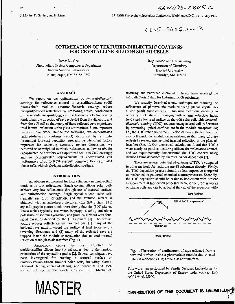
-. J. M. Gee, R. Gordon, and H. Liang 25’ IEEE Photovoltaic Specialists Conference, Washington, D.C., 13-17 May 1996 OPTIMIZATION OF TEXTURED-DIELECTRIC COATINGS FOR CRYSTALLINE-SILICON SOLAR CELLS James M. Gee Photovoltaic System Components Department Sandia National Laboratories Albuquerque, NM 87185-0752 ABSTRACT We report on the optimization of textured-dielectric coatings for reflectance control in crystalline-silicon (c-Si) photovoltaic modules. Textured-dielectric coatings reduce encapsulated-cell reflectance by promoting optical confinement in the module encapsulation; i.e., the textured-dielectric coating randomizes the direction of rays reflected from the dielectric and from the c-Si cell so that many of these reflected rays experience total internal reflection at the glass-air interface. Some important results of this work include the following: we demonstrated textured-dielectric coatings (ZnO) deposited by a high- throughput low-cost deposition process; we identified factors important for achieving necessary texture dimensions; we achieved solar-weighted extrinsic reflectances as low as 6% for encapsulated c-Si wafers with optimized textured-ZnO coatings; and we demonstrated improvements in encapsulated cell performance of up to 0.5% absolute compared to encapsulated planar cells with single-layer antireflection coatings. INTRODUCTION An obvious requirement for high efficiency in photovoltaic modules is low reflectance. Single-crystal silicon solar cells achieve very low reflectances through use of textured surfaces and antireflection coatings. Single-crystal silicon solar cells typically use (100) orientation, and the textured surface is obtained with an anisotropic chemical etch that etches (1 11) crystallographic planes much more slowly than the (100) planes. These etches typically use water, isopropyl alcohol, and either potassium or sodium hydroxide, and produce surfaces with four- sided pyramids defined by the (111) planes [l]. The surface texture reduces reflectance by two methods: (1) many of the incident rays must intercept the surface at least twice before reversing directions; and (2) many of the reflected rays are trapped inside the module encapsulation due to total internal reflection at the glass-air interface (Fig. 1). Anisotropic etches are less effective on multicrystalline-silicon (mc-Si) substrates due to the random orientation of the crystalline grains [2]. Several techniques have been investigated for creating a textured surface on multicrystalline-silicon (mc-Si) solar cells, including electro- chemical etching, chemical etching, and mechanical and laser- scribe texturing of the mc-Si substrate [3-61. Mechanical Roy Gordon and Haifan Liang Department of Chemistry Harvard University Cambridge, MA 02138 texturing and patterned chemical texturing have received the most attention to date for texturing mc-Si substrates. We recently described a new technique for reducing the reflectance of photovoltaic modules using planar crystalline- silicon (oSi) solar cells [7]. This new technique deposits an optically thick, dielectric coating with a large refractive index (n>2) and a textured surface on the c-Si solar cell. This textured- dielectric coating (TDC) reduces encapsulated-cell reflectance by promoting optical confinement in the module encapsulation; i.e., the TDC randomizes the direction of rays reflected fiom the c-Si cell inside the module encapsulation, so that many of these reflected rays experience total internal reflection at the glass-air interface (Fig. 1). Our theoretical calculations found that TDC’s were nearly as good as texturing silicon for reflectance control, and we experimentally demonstrated the TDC concept using diamond films deposited by chemical vapor deposition [7]. There are several potential advantages of TDC’s compared to other methods for texturing mc-Si substrates directly. Firstly, the TDC deposition process should be less expensive compared to mechanical or patterned chemical texture processes. Secondly, the TDC deposition should be easier to implement with present c-Si commercial fabrication processes because the process works on planar cells and can be added at the end of the sequence with- Front Swface Glass and Encapsulation Fig. 1. Illustration of confinement of rays reflected from a textured surface inside a photovoltaic module due to total internal reflection (TR) at the glass-air interface. This work was performed by Sandia National Laboratories for the United States Department of Energy under contract DE- AC04-94AL85000.
Transcript
-. J. M. Gee, R. Gordon, and H. Liang 25’ IEEE Photovoltaic Specialists Conference, Washington, D.C., 13-17 May 1996
OPTIMIZATION OF TEXTURED-DIELECTRIC COATINGS FOR CRYSTALLINE-SILICON SOLAR CELLS
James M. Gee Photovoltaic System Components Department
Sandia National Laboratories Albuquerque, NM 87185-0752
ABSTRACT We report on the optimization of textured-dielectric
coatings for reflectance control in crystalline-silicon (c-Si) photovoltaic modules. Textured-dielectric coatings reduce encapsulated-cell reflectance by promoting optical confinement in the module encapsulation; i.e., the textured-dielectric coating randomizes the direction of rays reflected from the dielectric and from the c-Si cell so that many of these reflected rays experience total internal reflection at the glass-air interface. Some important results of this work include the following: we demonstrated textured-dielectric coatings (ZnO) deposited by a high- throughput low-cost deposition process; we identified factors important for achieving necessary texture dimensions; we achieved solar-weighted extrinsic reflectances as low as 6% for encapsulated c-Si wafers with optimized textured-ZnO coatings; and we demonstrated improvements in encapsulated cell performance of up to 0.5% absolute compared to encapsulated planar cells with single-layer antireflection coatings.
INTRODUCTION An obvious requirement for high efficiency in photovoltaic
modules is low reflectance. Single-crystal silicon solar cells achieve very low reflectances through use of textured surfaces and antireflection coatings. Single-crystal silicon solar cells typically use (100) orientation, and the textured surface is obtained with an anisotropic chemical etch that etches (1 11) crystallographic planes much more slowly than the (100) planes. These etches typically use water, isopropyl alcohol, and either potassium or sodium hydroxide, and produce surfaces with four- sided pyramids defined by the (111) planes [l]. The surface texture reduces reflectance by two methods: (1) many of the incident rays must intercept the surface at least twice before reversing directions; and (2) many of the reflected rays are trapped inside the module encapsulation due to total internal reflection at the glass-air interface (Fig. 1).
Anisotropic etches are less effective on multicrystalline-silicon (mc-Si) substrates due to the random orientation of the crystalline grains [2]. Several techniques have been investigated for creating a textured surface on multicrystalline-silicon (mc-Si) solar cells, including electro- chemical etching, chemical etching, and mechanical and laser- scribe texturing of the mc-Si substrate [3-61. Mechanical
Roy Gordon and Haifan Liang Department of Chemistry
Harvard University Cambridge, MA 02138
texturing and patterned chemical texturing have received the most attention to date for texturing mc-Si substrates.
We recently described a new technique for reducing the reflectance of photovoltaic modules using planar crystalline- silicon (oSi) solar cells [7]. This new technique deposits an optically thick, dielectric coating with a large refractive index (n>2) and a textured surface on the c-Si solar cell. This textured- dielectric coating (TDC) reduces encapsulated-cell reflectance by promoting optical confinement in the module encapsulation; i.e., the TDC randomizes the direction of rays reflected fiom the c-Si cell inside the module encapsulation, so that many of these reflected rays experience total internal reflection at the glass-air interface (Fig. 1). Our theoretical calculations found that TDC’s were nearly as good as texturing silicon for reflectance control, and we experimentally demonstrated the TDC concept using diamond films deposited by chemical vapor deposition [7].
There are several potential advantages of TDC’s compared to other methods for texturing mc-Si substrates directly. Firstly, the TDC deposition process should be less expensive compared to mechanical or patterned chemical texture processes. Secondly, the TDC deposition should be easier to implement with present c-Si commercial fabrication processes because the process works on planar cells and can be added at the end of the sequence with-
Front Swface
Glass and Encapsulation
Fig. 1. Illustration of confinement of rays reflected from a textured surface inside a photovoltaic module due to total internal reflection (TR) at the glass-air interface.
This work was performed by Sandia National Laboratories for the United States Department of Energy under contract DE- AC04-94AL85000.
out any changes to the rest of the process. The other texture processes produce textured surfaces early in the cell fabrication sequence; this lextured surface can complicate some subsequent cell fabrication steps. Finally, the TDC process should be less damaging to the c-Si substrate compared to mechanical texturing. Nevertheless, these economical and technical require a material with suitable optical properties (transparent and large refractive index), and an inexpensive, high-throughput deposition process that produces films with a textured surface.
In this paper, we report on optimization of textured- dielectric coatings suitable for commercial production. The paper first discusses selection of materials for TDC’s that could be deposited by a low-cost deposition technique. The paper then discusses optimization of the TDC deposition conditions for optimal geometry. Finally, the optimized coatings were applied to complete solar cells.
EXPERlMENT The TDC requires the following properties: large refractive
index (n>2), low optical absorption between 0.35 and 1.2 pm, and a textured surface [7]. There has been considerable work on transparent conducting oxides (TCO) for thin-film photovoltaic modules. Some of the TCO materials investigated to date include tin oxide, indium tin oxide, titanium dioxide, and zinc oxide. These materials also have the appropriate optical properties for use as textured-dielectric coatings on c-Si solar cells, and can be deposited with high-throughput processes.
We investigated two materials: Ti02 and ZnO. The coatings were deposited in a custom-fabricated belt-furnace atmospheric-pressure chemical vapor deposition (CVD) reactor. The reactor uses a Watkims-Johnson gas injection nozzle that allows separate injection of two different gases through 10 cm- long parallel slots about 0.6 cm above the moving substrates. The Ti02 films were deposited at 4 5 0 T with titanium isopropoxide and water. The ZnO films were deposited at 25OOC using water and diethylzinc. The lower deposition temperature for the ZnO is an advantage because it allows the films to be deposited over metal grids more easily. A disadvantage of ZnO is the relatively low refractive index (around 2), while the Ti02 films have a more optimal refractive index (around 2.2). The belt speed was 1 inch per minute; two passes of the substrate through the deposition zone produced films about 2-pm thick. Thin films of Ti02 for antireflection coatings were deposited by electron- beam reactive evaporation.
The optical properties of the films were first optimized by depositing the films on polished silicon wafers. The hemisphe- rical reflectance of the coated samples were measured both before and after encapsulation with a commercial spectrophoto- meter. The sample encapsulation was performed in a custom laminator, and used low-iron glass and EVA similar to commercial photovoltaic modules.
We fabricated a set of large-area (42-cm2) cells with very uniform properties in the Photovoltaic Device Fabrication Laboratory (PDFL). These cells have planar surfaces and used 2- Rcm float-zone Q?Z) substrates. Half of these cells were then coated with optimized TDC films, and the cell performance was then measured both before and after encapsulation. High-quality processing and substrates were used for the experiment rather than commercial mc-Si cells in order to reduce statistical
2
uncertainties in comparing control cells with coated ceIls. The cell characteristics (one-sun current-voltage and spectral response and reflectance) were measured both before and after encapsulation.
RESULTS The Ti02 films were not adherent to the silicon wafers,
and work with Ti02 was discontinued early. We therefore emphasized textured-ZnO coatings. We deposited 2-pm thick, textured-ZnO films directly on silicon wafers and on silicon wafers with Ti02 antireflection coatings (ARC). Samples with Ti02 ARC’S were included because the refractive index of ZnO is less than optimal for our TDC application. Figure 2 shows the as-deposited and encapsulated hemispherical reflectance of these samples, along with our theoretical fit. The theoretical fit used a
Zn OISi l i con
300 500 700 900 1100 I Wavelength (nrn)
Zn01TiOZSilicon
0.25 , I I t l l I I I “I
i,
O.1°
0.05
0.00 300 500 700 900 1100
Wavelength (nrn)
Fig. 2. Comparison of measured hemispherical reflectance (Data) and theoretical fits (Model) of as-deposited and encapsulated wafers with textured-ZnO coatings: textured- ZnO deposited over silicon (ZnO/Silicon), and textured-ZnO deposited over TiOZcoated silicon (ZnO/Ti02/Silicon). There is a large discrepancy between Model and Data for short wavelengths (< $00 nm) because the model calculations do not include absorption in the optical coatings or in the encapsulant.
DISCLAIMER
Portions of this document may be illegible in electronic image products. Images are produced from the best available original document.
DISCLAIMER
This report was prepared as an account of work sponsored by an agency of the United States Government. Neither the United States Government nor any agency thereof, nor any of their employees, makes any warranty, exprtss or implied, or assumes any legal liability or responsibility for the accuracy, completeness, or use- fulness of any information, apparatus, product, or process disclosed, or represents that its use would not infringe privately owned rights. Reference herein to any spe- cific commercial product, process, or service by trade name, trademark, manufac- turer, or otherwise does not necessarily constitute or imply its endorsement, recom- mendation, or favoring by the United States Government or any agency thereof. The views and opinions of authors expressed herein do not necessarily state or reflect those of the United States Government or any agency thereof.
J. M. Gee, R. Gordon, and H. Liang 25" IEEE Photovoltaic Specialists Conference, Washington, D.C., 13-17 May 1996
rig. 5 SCM pnoromicrograpns 01 rexrurea-mu nims deposited on silicon (ZnOlSi) and on Ti02-coated silicon (Zn/TiO2/Si).
thick-film optical model of photovoltaic modules th2t was described previously [7]. The theoretical fit used published dispersion data for the ZnO [SI. The dispersion data for the Ti02 films was measured in our laboratory [9]. The only adjustable parameter in the model was the percentage of light reflected from the glass-ZnO interface that experienced double-bounce reflectance.
The reflectance of the ZnO/Si sample actually increased after encapsulation and the theoretical fit was poor. The fit for the ZnORi02/Si samples was quite good and achieved encapsulated solar-weighted extrinsic reflectance's as low as 6%. (Extrinsic reflectance only includes photons reflected from the front surface of the c-Si solar cell, and does not include weakly absorbed photons (wavelengths > 1000 nm) reflected from the back surface of the c-Si solar cell.) The encapsulated solar- weighted reflectance of 6% is a significant improvement compared to the present commercial process for mc-Si
photovoltaic modules, which use planar-surface silicon cells with a single-layer ARC and have encapsulated solar-weighted active- area reflectances around 9-12% [lo]. The encapsulated solar- weighted reflectance of the textured-Zn0 samples also approach the value of encapsulated textured single-crystal silicon samples (around 5%) [lo].
An important element in the optimization of the TDC deposition is achieving sufficiently large texture dimensions for optical scattering. Scanning electron microscopy (SEM) photomicrographs show that both ZnO/Si and ZnORiO2/Si films exhibited columnar growth (Figure 3), which indicates that the texture dimensions are controlled by the initial nucleation of the deposition. The ZnO/Si films were dense with a feature size around 0.5 pm, while the ZnO/Ti02/Si films were more porous and had a feature size around 1 pm. The light scattering from the ZnO/Si surface is not fully Lambertian (Le., reflected rays do not fill 271 hemisphere) over much of the solar spectrum due to the small feature size; the net result is that the encapsulated reflectance of the ZnO/Si increased because fewer rays reflected from the cell were optically confined in the encapsulation. The larger texture dimensions of the ZnO/Ti02/Si samples produced a more Lambertian scattering, which improved both the model fit and the optical performance.
The Ti02 ARC is not expected to be a problem in production because it can be deposited in the same belt- furnace CVD reactor with the textured-ZnO coating. Because the Ti02 film is necessary to obtain the proper texture dimensions, we performed a series of calculations to optimize the Ti02 films (Figure 4). These calculations also considered a thin Si02 layer between the Ti02 film and the silicon surface; these thin Si02 layers are commonly used for surface passivation. These calculations used a commercial ray-tracing program rather than our thick-optics model in order to include absorption in the thin films. The calculations indicate that a thicker Ti02 film is required than typically used for planar encapsulated cells.
I I I I I 0 10 P 30
sa2
Fig. 4. Calculated solar absorptance (short-circuit current density with units of mA/cm2) as a function of Ti02 and Si02 thicknesses for encapsulated planar c-Si cells with a textured-ZnO coating. CalcuIations used a. commercially available ray tracing program (Sunrays 111 I).
3
* ’ b
25” IEEE Photovoltaic Specialists Conference, Washington, D.C., 13-17 May 1996
35
30---
J. M. Gee, R Gordon, and H. Liang
I l l I I I I I + + + %
I l l I I I I +I*
~ - - _ L _ - I _ - _ L - - L - _ - I - - - L - - ~ I I I I I I I ufp.; -, _ _ _ _ _ I _ _ - - - - - n - - -
0
E” 15
10
5
2
I I I I I I I I 0 I 300 400 500 600 700 800 900 loo0 1100 12W
Wavelength (nm)
Fig. 5. Hemispherical reflectance spectra of encapsulated planar cells with and without textured-ZnO coating.
reflectance of around 9% compared to 14% for the encapdated planar cells. The encapsulated cells with textured-ZnO coating have fairly flat spectral reflectance characteristics, and are dark gray in appearance. Note that the reflectance minima were at relatively long wavelengths, which indicates that the Ti02 ARC was thicker than desired in these particular cells.
CONCLUSIONS We presented results of a study to optimize textured-
dielectric coatings for reflectance control in photovoltaic modules. The study found that the coatings are quite effective
optically, can be deposited with acceptable optical properties and with commercially relevant, high-throughput processes, and confirmed their performance advantages in complete encapsulated cells.
ACKNOWLEDGEMENTS E. Buck, B. Silva, and J. Tingley fabricated the cells, L.
Irwin and K. Snyder performed the reflectance measurements and cell characterization, and T. Hund performed the cell tabbing and encapsulation.
1.
2.
3.
4.
5.
6.
7.
8. 9.
REFERENCES D.L. King and M.E. Buck, “Experimental Optimization of an Anisotropic Etching Process for Random Texturization of Silicon Solar Cells,” 22nd ZEEE PVSC, 1991, pp. 303- 308 (1991). J.M. Gee et af., “The Effect of Encapsulation on the Reflectance of Photovoltaic Modules using Textured Multicrystalline-Silicon Solar Cells,” Ist World Con$ on Photo. Energy Conv., 1994, pp. 1555-1558. Y. S. Tsuo, et al., “Potential Applications of Porous Silicon in Photovoltaics,” 23rdIEEE PVSC, 1992, pp. 287-293. M.J. Stocks, J.J. Carr, and A.W. Blakers, “Texturing of Polycrystalline Silicon,” 1st World Con$ on Photo. Energy
S . Narayanan, et al., “18% Efficiency Polycrystalline Silicon Solar Cells,” 21st IEEE PVSC, 1990, pp. 678-680. P. Fath, et aL, “Mechanical Wafer Engineering for High Efficiency Solar Cells: An Investigation of the Induced Surface Damage,” 1st World Conf: on Photo. Energy Conv.,
J.M. Gee, R. Gordon, and H. Liang, “Reflectance Control for Multicrystalline-Silicon Photovoltaic Modules using Textured-Dielectric Coatings,” 1st World Con$ on Photo. Energy Conv., 1994, pp. 1274-1277. Brett and Parsons, Solid State Comm. 54,604-606 (1985). H. L. Tardy, Sandia National Laboratories, private communication.
C O ~ V . , 1994, pp. 1551-1554.
1994, pp. 1347-1350.
10. J. M. Gee et al., “The effect of encapsulation on the reflectance of photovoltaic modules using textured multicrystalline-silicon solar cells,” 1st World Con$ on Photo. Energy Conv., 1994, pp. 1555-1558.
11 . R Brendel, “Sunrays: A Versatile Ray Tracing Program for the Photovoltaic Community,” 12th Eur. Photo. Sol. Energy Con$, 1994, pp. 1339-1342.