Evaluation of Data Retention and Imprint Characteristics of FRAMs Under Environmental Stresses for NASA Applications Ashok K. Sharma/NASA-GSFC Goddard Space Flight Center, Greenbelt, MD 20771 Ashok.K.Sharma. 1 @,gsfc.nasa.gov Alexander Teverovsky/QSS/Goddard Operations Goddard Space Flight Center, Greenbelt, MD 20771 Alexander.Teverovskv@gs fc.nasa.gov Terry W. DowdyNAVSEA Crane Brett HamiltodNAVSEA Crane Abstract A major reliability issue for all advanced nonvolatile memory (NVM) technology devices including FRAMs is the data retention characteristics over extended period of time, under environmental stresses and exposure to total ionizing dose (TID) radiation effects. For this testing, 256 Kb FRAMs in 28-pin plastic DIPS, rated for industrial grade temperature range of -40 "C to +85 "C, were procured. These are two-transistor, two-capacitor (2T-2C) design FRAMs. In addition to data retention characteristics, the parts were also evaluated for imprint failures, which are defined as the failure of cells to change from a "preferred" state, where it has been for a significant period of time to an opposite state (e.g., from 1 to 0, or 0 to 1). These 256 K FRAMs were subjected to scanning acoustic microscopy (C-SAM); 1,000 temperature cycles from -65 "C to +150 "C; high temperature aging at 150 "C, 175 "C, and 200 "C for 1,000 hours; highly accelerated stress test (HAST) for 500 hours; 1,000 hours of operational life test at 125 OC; and total ionizing dose radiation testing. As a preconditioning, 10 K read/write cycles were performed on all devices. Interim electrical measurements were performed throughout this characterization, including special imprint testing and final electrical testing. Some failures were observed during high temperature aging test at 200 "C, during HAST testing, and during 1,000 hours of operational life at 125 "C. The parts passed 10 Krad exposure, but began showing power supply current increases during the dose increment from 10 Krad to 30 Krad, and at 40 Krad severe data retention and parametric failures were observed. Failures from various environmental group testing are currently being analyzed. Table of Contents 1 .o 2.0 3 .O 4.0 5 .o 6.0 INTRODUCTION BACKGROUND TEST PLAN ENVIRONMENTAL AND RADIATION TESTING DATA RETENTION AND IMPRINT TEST SUMMARY ACKNOWLEDGEMENT 1.0 INTRODUCTION Ferroelectric random access memories (FRAMs) are very attractive for space applications because of their nonvolatile characteristics, low power consumption, high operational speeds, and readlwrite cycling endurance specifications in tens of billions. FRAMs have two orders of magnitude less write access time and require three orders of magnitude less energy per bit write compared to conventional nonvolatile memory devices (EEPROMs and/or Flash Memory). FRAMs density has also improved significantly over the last few years, driven by a variety of commercial applications. The first 4 Kb commercially available FRAMs were manufactured by Ramtron less than 10 years ago, and now memory densities of 1 Gb based on 0.18 pm technology appear to be technically feasible [I]. An area of high interest in NVMs has been the development of thin-film FE technology to build FRAMs. However, these FE films used as memory storage elements have significant reliability concerns such as aging/fatigue effects from a large number of polarization reversal cycles, thermal stability, effects of electric field, and time dependent dielectric breakdown (TDDB) PI. https://ntrs.nasa.gov/search.jsp?R=20030036989 2018-09-07T02:27:03+00:00Z
Transcript
Evaluation of Data Retention and Imprint Characteristics of FRAMs Under Environmental
Stresses for NASA Applications Ashok K. Sharma/NASA-GSFC
Goddard Space Flight Center, Greenbelt, MD 20771 Ashok.K.Sharma. 1 @,gsfc.nasa.gov
Alexander Teverovsky/QSS/Goddard Operations Goddard Space Flight Center, Greenbelt, MD 20771
Alexander.Teverovskv@gs fc.nasa.gov
Terry W. DowdyNAVSEA Crane Brett HamiltodNAVSEA Crane
Abstract
A major reliability issue for all advanced nonvolatile memory (NVM) technology devices including FRAMs is the data retention characteristics over extended period of time, under environmental stresses and exposure to total ionizing dose (TID) radiation effects. For this testing, 256 Kb FRAMs in 28-pin plastic DIPS, rated for industrial grade temperature range of -40 "C to +85 "C, were procured. These are two-transistor, two-capacitor (2T-2C) design FRAMs. In addition to data retention characteristics, the parts were also evaluated for imprint failures, which are defined as the failure of cells to change from a "preferred" state, where it has been for a significant period of time to an opposite state (e.g., from 1 to 0, or 0 to 1). These 256 K FRAMs were subjected to scanning acoustic microscopy (C-SAM); 1,000 temperature cycles from -65 "C to +150 "C; high temperature aging at 150 "C, 175 "C, and 200 "C for 1,000 hours; highly accelerated stress test (HAST) for 500 hours; 1,000 hours of operational life test at 125 O C ; and total ionizing dose radiation testing. As a preconditioning, 10 K read/write cycles were performed on all devices. Interim electrical measurements were performed throughout this characterization, including special imprint testing and final electrical testing. Some failures were observed during high temperature aging test at 200 "C, during HAST testing, and during 1,000 hours of operational life at 125 "C. The parts passed 10 Krad exposure, but began showing power supply current increases during the dose increment from 10 Krad to 30 Krad, and at 40 Krad severe data retention and parametric failures were observed. Failures from various environmental group testing are currently being analyzed.
Table of Contents
1 .o 2.0 3 .O 4.0 5 .o 6.0
INTRODUCTION BACKGROUND TEST PLAN ENVIRONMENTAL AND RADIATION TESTING DATA RETENTION AND IMPRINT TEST SUMMARY ACKNOWLEDGEMENT
1.0 INTRODUCTION
Ferroelectric random access memories (FRAMs) are very attractive for space applications because of their nonvolatile characteristics, low power consumption, high operational speeds, and readlwrite cycling endurance specifications in tens of billions. FRAMs have two orders of magnitude less write access time and require three orders of magnitude less energy per bit write compared to conventional nonvolatile memory devices (EEPROMs and/or Flash Memory). FRAMs density has also improved significantly over the last few years, driven by a variety of commercial applications. The first 4 Kb commercially available FRAMs were manufactured by Ramtron less than 10 years ago, and now memory densities of 1 Gb based on 0.18 pm technology appear to be technically feasible [I].
An area of high interest in NVMs has been the development of thin-film FE technology to build FRAMs. However, these FE films used as memory storage elements have significant reliability concerns such as aging/fatigue effects from a large number of polarization reversal cycles, thermal stability, effects of electric field, and time dependent dielectric breakdown (TDDB) PI.
One of the major reliability issues for all nonvolatile memory devices, FRAM included, is data retention, which is defined as the ability of a memory device to maintain stored data between the time of writing and subsequent reading of the stored information. Temperature significantly accelerates retention failures due to thermal depolarization of the poled state in the ferroelectric material and is commonly used to accelerate this failure mechanism. Evaluation of low density Ramtron FRAMs has demonstrated a failure rate of less than 60 FITS with a 60% confidence level for 10-year data storage at room temperature [3]. However, data retention characteristics depend on manufacturing processes as well as design factors and remain a major reliability concern for new generations of FRAMs.
Another degradation mechanism, which is known to affect reliability of ferroelectric memories is fatigue. Fatigue in ferroelectric materials is a decrease of switchable polarization with an increased number of switching cycles or polarization reversals. This degradation process is related to the electrode interfacial areas of the memory cells and can be significantly decreased by using appropriate electrode materials, for example RuOzPZT structures, instead of FWZT structures [4]. The electric-field-assisted migration of charged species (most likely oxygen vacancies) within ferroelectric materials may be also responsible for the degradatiodfatigue behavior [5], [6].
In addition to retention and fatigue failures, other failure modes and mechanisms such as aging, imprint, and reducing environment degradation are known to be specific to ferroelectric memory cells. Aging is defined as a mechanism that causes signal loss during a retention period, which does not recover after a rewrite and immediate read. This differentiates it from the retention failures, where a signal recovers after rewrite and immediate read. Aging is considered as a gradual stabilization of the domain structure due to which the ferroelectric becomes less responsive to applied fields [7], [SI. Imprint is a phenomenon specific to the ferroelectric materials. Once a capacitor has spent significant time in one polarity, it is reluctant to switch polarities [9]. This effect is due to accumulation of charges with time in the ferroelectric cell, which compensates the created polarization.
Annealing of Pt/PZT system in a hydrogen-containing ambient (e.g., forming gas) might cause severe degradation of PZT thin film [lo]. Hydrogen that reaches the platinum-PZT interface is a strong enough reducing agent, with Pt as a catalyst, to take oxygen from the lead lattice of the PZT. This results in forming a water molecule, which reduces the adhesion between the PZT and platinum and degrades the signal from the ferroelectric cell. It was shown [ 1 11 that the hydrogen evolved from plastic packaging during molding, and post-mold cure can affect data retention reliability of FRAMs. Another mechanism of polarization suppression in PZT films is related to high temperature reducing treatments in dry nitrogen at 400 "C [12]. This treatment creates oxygen vacancies, which might lock domains. The trapped charges are believed to inhibit the domain motion and cause failures of memory cells.
Although ferroelectric films have shown high radiation tolerance, results of total dose radiation testing of commercial FRAMs have shown these devices to be failing at 10 Krad and higher TID. Also, these FRAMs can typically latch up under relatively low energy heavy ion exposure. This is primarily due to radiation softness of underlying commercial processes used to fabricate these memories. For this evaluation, only TID testing was performed.
Ferroelectric memory is a relatively new, emerging technology, which requires in-depth understanding of the related reliability issues and extensive testing at extreme conditions for space applications. The objective of this work was to evaluate reliability of commercial 256 Kb FRAMs over a wide temperature range with a focus on data retention and imprint characteristics.
2.0 BACKGROUND
In the NVMTS 2001, data retention and fatigue characteristics were reported of 64 Kb PZT-based FRAMs, tested over a temperature range from -85 "C to +310 "C for ceramic packaged parts and from -85 "C to +175 "C for plastic parts, during retention periods of up to several thousand hours. The observed data retention failures were divided into three categories: (1) random failures that were not related to stress conditions, (2) weak cell failures, which were also not related to a particular stress condition but were reproducible from test to test, and (3) intrinsic failures that were caused by thermal degradation (or wearout) of the ferroelectric cell material. A conclusion was that additional testing should be performed on higher density 256 Kb FRAMs.
3.0 TESTPLAN
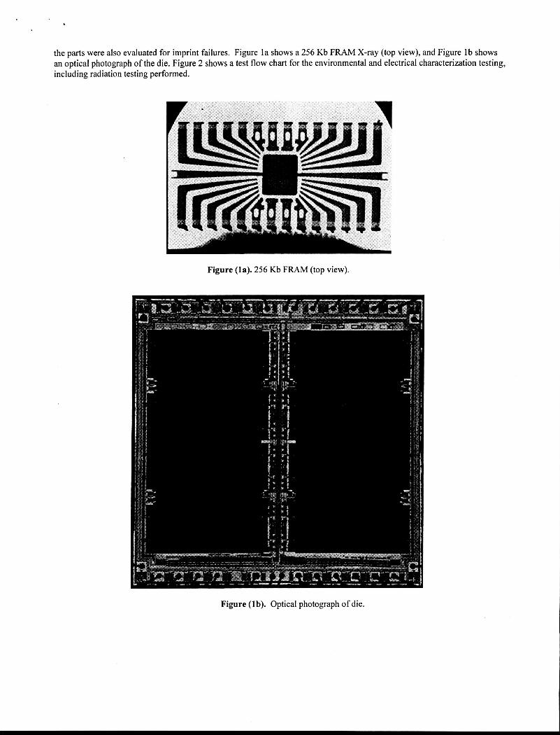
For this testing, 256 Kb FRAMs in 28-pin plastic DIPS, rated for industrial grade temperature range of -40 O C to +85 "C, were procured. These are two-transistor, two-capacitor (2T-2C) design FRAMs. In addition to data retention characteristics,
the parts were also evaluated for imprint failures. Figure la shows a 256 Kb FRAM X-ray (top view), and Figure l b shows an optical photograph of the die. Figure 2 shows a test flow chart for the environmental and electrical characterization testing, including radiation testing performed.
Figure (la). 256 Kb FRAM (top view).
Figure (lb). Optical photograph of die.
I
I
Notes:
1.
2.
3.
4. 5.
6.
7. 8.
Figure 2. Test flow chart.
Two devices were sent for Construction Analysis (CA) before environmental testing. All devices were sent for C-SAM before and after tests, Full electrical testing included input and output voltages and leakage currents, stand-by and active power supply currents, and chip enable access time. W/RO, W/R1, W R CB, W/R Inverted CB, and W/R Random were included in a full WriteRead. Temperature cycling was at temperatures -65 "C to 150 "C with 15 minute dwell at each extreme and 10, 40,50, 100 cycles up to 1,000 cycles total. The total transfer time from hot to cold did not exceed 1 minute. HAST was unbiased with five 100 hour test segments. High Temperature Operating Life (HTOL) was dynamic. Electrical endpoints were at 250,500 and 1000 hours. For the temperature exposure test, lots were divided for three temperatures: 150 "C, 175 "C, and 200 "C. Electrical endpoints were at 100,500, and 1,000 hours. Total Dose Radiation Testing was performed in test segments at lK, 3K, 5K, IOK, 20K, and 30K. For each environmental step, a special test to detect imprint failures recommended by the manufacturer was performed. The test consisted of write pattern, bake-out at 70 "C for 15 minutes, and readkerifl pattern during each interim and final electrical measurements.
4.0 ENVIRONMENTAL AND RADIATION TESTING
Visual/Serialization
All 97 devices were visually inspected, serialized, and sent to C-mode Scanning Acoustic Microscopy (C-SAM). All devices passed visual inspection and C-SAM.
Preconditioning
Ninety-five devices were given 10,000 R e a m r i t e cycles prior to environmental tests.
Electrical Testing
Parametric measurements of I/O voltages, leakage currents (VOL, VOH, VIL, VIH, ILI, ILO), and Clock Enable Access time were made after every test increment. All electrical tests were performed at 25 "C. Retention tests (W/RO, W R l , CB, Inverted CB, and W/R Random) were performed after every test increment. The devices were then baked at 70 "C for 15 minutes and the electrical and retention tests were repeated.
Temperature Cycling
Serial numbers 1-20 were tested as per MIL-STD-883, Method 1010, condition B (except the cold temperature was at -65 "C) for 1,000 cycles. Electrical tests were performed after every 100 cycles. Test lot did not experience any failures.
Highly Accelerated Stress Test (HAST)
This test was performed on S N s 21-40 with 500 hours of 130 "C at 85% RH at 2 atm in 100-hour intervals. S/Ns 3 1 and 37 experienced hard electrical failures after 400 hours. Multiple devices had memory read failures during the 500 hours of HAST, but were able to be rewritten.
High Temperature Operating Life (HTOL)
This test was performed on serial numbers 41-60 for 1,000 hours with endpoints taken at 250, 500, and 1,000 hours. The voltage level was set at 5.5 V at 125 "C. S / N 46 failed read 1 and CB after 500 hours. Other devices failed various memory reads, but were able to be rewritten.
High Temperature Exposure Aging
Twenty-four devices ( S N s 61-84) were exposed to accelerated temperature aging at 150 "C, 175 "C, and 200 "C. Eight devices were exposed to each temperature. Electrical endpoints were taken at 250 hrs., 500 hrs., and 1,000 hrs. Testing was stopped after failures were noted at the 200 "C temperature after 500 hours of exposure. No failures occurred at 150 "C and 175 "C.
Total Dose Radiation Test
For radiation testing, Gamma Cell 220 was used at a dose rate of 83.3 radsec. A total of six devices in the test lot were irradiated under static bias, and one device was used as a control sample. HP82000 Automatic Test Equipment (ATE) was used for all the required functional and power supply tests that included random read, active current, standby current, input leakage current, VOL, VOH, Clock Enable Access time, 0 pattern write, 1 pattern write, checkerboard write, and random write tests.
All devices remained functional through 10 Krad but began showing power supply current increases during the dose increment from 10 Krad to 30 Krad (see Table 2). Inthe post 30 Krad electrical test, all parts showed increased power supply currents (combined currents rising from 1.24 ma to 0.263 A during irradiation) and one part ( S / N 90) showed complete electrical and data retention failure. After 40 Krad, the remaining five test parts showed severe data retention and parametric failure as evidenced by electrical test failure ( 9 " s 86,88, and 89). Serial number 85 failed the random read test. Annealing for one day (room temperature anneal with bias applied and 70 "C heated anneal without bias) showed a small amount of parametric recovery, but the power supply parametric and data retention failures remained.
Table 1 provides a summary of environmental and electrical characterization including radiation test results.
Table 1. Environmental, electrical, and radiation test results summary.
Test I Test Condition I Qty. I Failed I Rem arks
Exp.
Exp.
200 "C Temp. Exp.
Total Dose Rad.
175 "C Temp.
~~
Temp. Cycling
1,000 hrs. 8 0
All eight devices passed electrical endpoints after
after 500 hours. Testing was stopped after 500 hours.
failed after 30 Krads.
1,000 hrs. 8 8 100 hours but failed various electrical endpoints
6 6 Devices passed exposures through 20 Krads but
HAST
Total Retention 150 O C Time Test Failed Failed (hrs.) (hrs.) Parts Vectors 100 100 018 0 500 400 018 0 1000 500 018 0
HTOL
200 OC 175 O C Failed Failed Failed Failed Parts Vectors Parts Vectors
S I N S 31 & 37 failed various electrical endpoints at 400 hours and were not able to be reprogrammed. Other devices had memory read failures after HAST but were able to be reprogrammed. S I N 46 failed read 1 and CB after 500 hours and could not be reprogrammed. Other devices failed various memory reads, but were able to be reprogrammed.
5.0 DATA RETENTION AND IMPRINT TEST SUMMARY
Temperature cycling can potentially degrade the retention characteristics of FRAMs. However, temperature cycling performed on 20 FRAM sample devices for 1,000 cycles as per test conditions shown in Figure 2 test flow showed no data retention or imprint failures.
HAST was performed on 20 FRAM sample devices as per Figure 2 test flow. Test results showed multiple devices failing post HAST interim and final electrical measurement read test but were able to be reprogrammed, indicating data retention failures. Two devices experienced hard failures after 400 hours of HAST testing. HTOL test was performed on 20 FRAM sample devices that were subjected to 1,000 hours life test at 125 "C as per Figure 2 test flow. Test results showed multiple devices failing interim and final post HTOL electrical measurements read test but were able to be reprogrammed, indicating data retention failures. One device was a hard failure and could not be reprogrammed. No imprint test failures were observed during HAST or HTOL testing. Two HAST failures and one HTOL failure are undergoing analysis including C-SAM inspection.
Twenty-four devices were subjected to high temperature exposure aging at 150 "C, 175 "C, and 200 "C. Eight devices were exposed to each temperature. Electrical endpoints were taken at 250 hrs., 500 hrs., and 1,000 hrs. No failures occurred at 150 "C and 175 "C. Testing was stopped after failures were observed at the 200 "C temperature after 500 hours of exposure, and these failures could not be reprogrammed. Some of these failures are being subjected to additional analysis. Table 2 shows high temperature exposure aging test summary, and Figure 3 shows the time versus % of failed vectors for three temperatures testing.
- - Temp Exposure
O
1 uu
10
1
0.1
0.01
0.001
~.0001
+ 150C -+- 175C
1 -c- 200c
1 10 100
time, hr
1000
~~
Figure 3. High temperature exposure aging test curves.
During total dose radiation testing, all devices remained functional through 10 Krad but began showing power supply current increases during the dose increment from 10 Krad to 30 Krad (see Table 3). During the post 30 Krad electrical test, all parts showed increased power supply currents and one part showed complete electrical and data retention failure. Afler 40 Krad, the remaining five test parts showed severe data retention and parametric failures. One day anneal showed a small amount of parametric recovery, but the power supply parametric and data retention failures remained.
Table 3. Summary of total dose failures.
(**refers to A8 and A9 and determines the one of four columns within each block)
6.0 ACKNOWLEDGEMENT
Acknowledgment is due to NAVSEA, Crane, Indiana, for providing environmental and electrical test support.
References
r 11
r21 [31
r41
151
r71
r61
P I
A. Sheikholeslami and P. Gulak, “A survey of circuit innovations in ferroelectric memories,” Proc. IEEE, Vol.
A. K. Sharma, Semiconductor Memories: Technolow, Testing and Reliabilitv, IEEE Press, New York, 1996. E. M. Philofsky, “FRAM-the ultimate memory,” Sixth Biennial IEEE International Nonvolatile Memory Technology Conference, 1996, pp. 99-104. J. J. Lee, et al., “Electrode contacts on ferroelectric PZT and SBT thin films and their influence on fatigue properties,” J. Appl. Phys, Vol. 78, No. 8, 1995, pp. 5073-5077. J. Chen, et al., “Compositional control of ferroelectric fatigue in pervoskite ferroelectric ceramics and thin films,” J. Appl. Phys, Vol. 76, No. 9, 1994, pp.5394-5398. J. Chen, et al., “Polarization fatigue in pervoskite ferroelectric ceramics and thin-films,” Proceedings of the Eighth IEEE International Symposium on Applications of Ferroelectrics, ISAF ‘92, 1992, pp. 11 1-1 15. D. E. Fisch, et al., “Analysis of thin film ferroelectric aging,” IEEE, IRPS, 1990, pp. 237-242. A. Gregory, et al., “Thermal stability of ferroelectric memories,” 30th Annual Proceedings, International
88, NO. 5,2000, pp. 667-689.
Reliability Physics Symposium, 1992, pp. 91-94. [9] D. Hadnagy, “Making ferroelectric memories,” The Industrial Physicist, Dec. 1999, pp.26-28. [lo] W. S. Kim, et al., “Fabrication and characterization of Pt-oxide electrode for FeRAM application,” International
Conference Microprocesses and Nanotechtplogy, 2000, pp. 186-1 87. [11]E. M. Philofsky, et al., “The evolution of hydrogen from plastic molding compound and its effect on yield and
reliability of ferroelectric memories,” 36th Annual Proceedings, International Reliability Physics Symposium, 1998, pp. 232-237.
pp. 6695-6701. [12] W. L. Warren, et al., “Polarization suppression in Pb(Zr,Ti)03 thin films,” I. Appl. Phys, Vol. 77, No. 12, 1995,
Biographies
Ashok Sharma. Ashok Sharma received his B.S. in physics while in India and his BSEE and MSEE from Catholic University of America in Washington, DC. He has 20 years’ experience in semiconductor microelectronics reliability engineering and space flight projects quality assurance support activities. He has written several technical reports and papers for IEEE publications and is author of several books, including Semiconductor Memories published by IEEE, Programmable Logic Handbook published by McGraw Hill, Inc., and a book on Advanced Semiconductor Memories scheduled for publication later this year.
Alexander Teverovsky. Alexander Teverovsky received his Ph.D. in electrical engineering from Moscow University of Electronics, Russia. He has worked in the Moscow Institute of Electronic Machine Building and specializes in reliability physics of semiconductor devices. Currently, he is involved in several projects aimed toward evaluating new technologies and components for space applications.