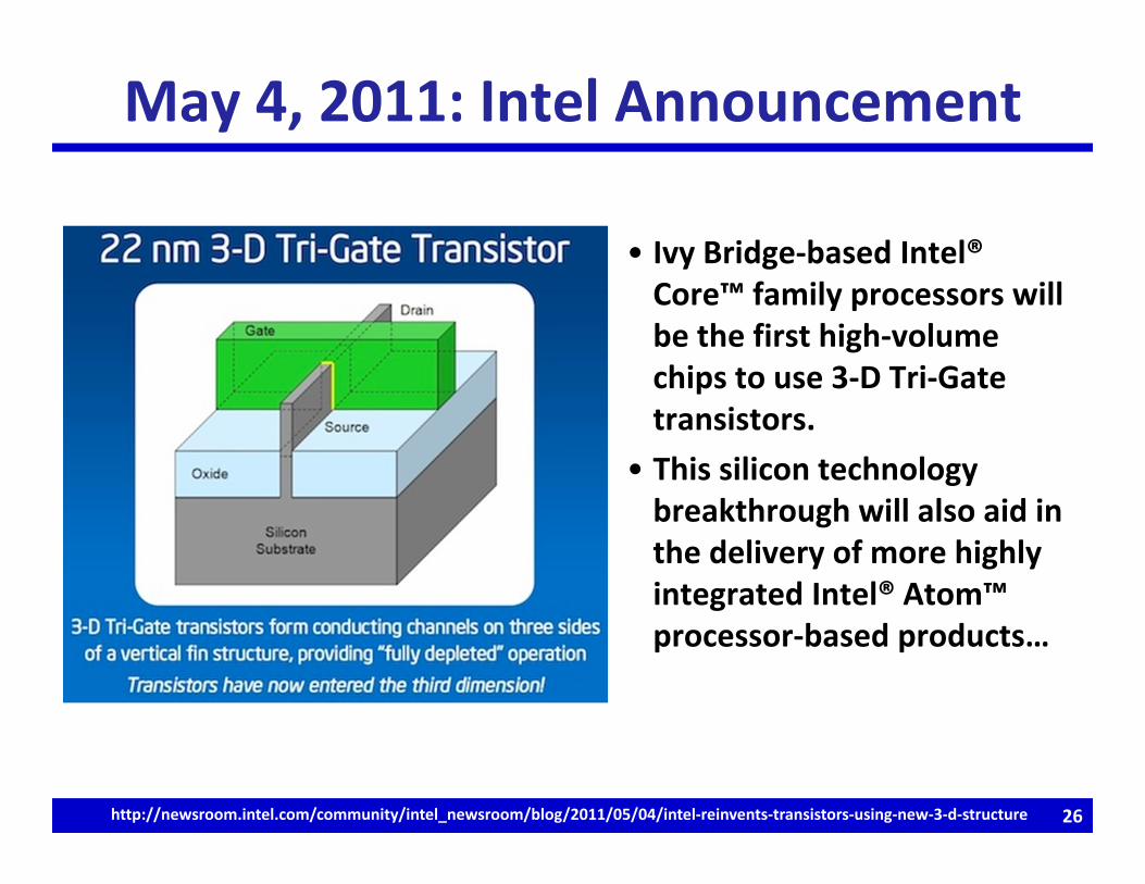
On May 4, 2011, Intel Corporation announced what it called the most radical shift in semiconductor technology in 50 years. A new 3‐dimensional transistor design will enable the production of integrated‐circuit chips that operate faster with less power… The 3‐D Tri‐Gate transistor is a variant of the FinFET developed at UC‐Berkeley, and is being used in Intel’s 22nm‐ generation microprocessors.
Transcript
On May 4, 2011, Intel Corporation announced what it called the most radical shift in semiconductor technology in 50 years. A new 3‐dimensional transistor design will enable the production of integrated‐circuit chips that operate faster with less power…
The 3‐D Tri‐Gate transistor is a variant of the FinFET developed at UC‐Berkeley, and is being used in Intel’s 22nm‐generation microprocessors.
Lecture 28
OUTLINE
CMOS Technology Advancement
• The CMOS power crisis
• Advanced MOSFET structures
– Thin‐body MOSFET structures
– History and future of multi‐gate MOSFETs
Reading: Hu 7.8
Historical Voltage Scaling• Since VT cannot be scaled down aggressively, the supply voltage (VDD) has not been scaled down in proportion to the MOSFET gate length:
Source: P. Packan (Intel), 2007 IEDM Short Course
VDD
VDD – VT
3
Power Density Scaling – NOT!Po
wer Den
sity (W/cm
2 )
1E‐05
1E‐04
1E‐03
1E‐02
1E‐01
1E+00
1E+01
1E+02
1E+03
0.01 0.1 1
Gate Length (μm)
Passive Power Density
Active Power Density
Source: B. Meyerson (IBM) Semico Conf.,January 2004
Power Density Trend
400480088080
8085
8086
286 386486
Pentium® procP6
1
10
100
1000
10000
1970 1980 1990 2000 2010Year
Power Den
sity (W
/cm
2 )
Hot Plate
Nuclear Reactor
Rocket Nozzle
Source: S. Borkar (Intel )
Sun’s Surface
Power Density Prediction circa 2000
4
Parallelism
• Computing performance is now limited by power dissipation. This has forced the move to parallelism as the principal means of increasing system performance.
400480088080
8085
8086
286 386 486Pentium® proc
P6
1
10
100
1000
10000
1970 1980 1990 2000 2010Year
Pow
er D
ensi
ty (W
/cm
2)
Hot Plate
Nuclear Reactor
Rocket NozzleSun’s Surface
Core 2
Source: S. Borkar (Intel )100 101 102 103 1040
20
40
60
80
100
Nor
mal
ized
Ene
rgy/
op1/throughput (ps/op)
Operate at a lower energy point (lower VDD)
Run in parallel to recoup performance
singlecore
dualcore
Energy vs. Delay per operation
5
Intel Ivy Bridge Processor
6
CMOS Technology Scaling
• Gate length has not scaled proportionately with device pitch (0.7x per generation) in recent generations.– Transistor performance has been boosted by other means.
90 nm node 65 nm node 45 nm node 32 nm node
T. Ghani et al.,IEDM 2003
K. Mistry et al.,IEDM 2007
P. Packan et al.,IEDM 2009
XTEM images with the same scale courtesy V. Moroz (Synopsys, Inc.)
(after S. Tyagi et al., IEDM 2005)
7
MOSFET Performance Boosters
P. Packan et al., IEDM Technical Digest, pp. 659‐662, 2009
• Strained channel regions eff
• High‐k gate dielectric and metal gate electrodes Cox
Cross-sectional TEM views of Intel’s 32nm CMOS devices
8
Key to VDD Reduction: Gate Control
• The greater the capacitive coupling between Gate and channel, the better control the Gate has over the channel potential.
lower VDD to achieve target ION/IOFF
reduced short‐channel effect (SCE) and drain‐induced barrier lowering (DIBL)
9
log ID
VGSVDD
ION
Body
Gate
Drain
CoxCdep
Sourceox
total
CCS
Why New Transistor Structures?• Off‐state leakage (IOFF) must be suppressed as Lg is scaled down
– allows for reductions in VT and hence VDD
• Leakage occurs in the region away from the channel surface Let’s get rid of it!
DrainSource
Gate
LgThin‐BodyMOSFET:
Buried Oxide
Source Drain
Gate
Substrate
“Silicon‐on‐Insulator” (SOI)
Wafer
10
Thin‐Body MOSFETs• IOFF is suppressed by using an adequately thin body region.
– Body doping can be eliminated higher drive current due to higher carrier mobility
DELTA MOSFETD. Hisamoto, T. Kaga, Y. Kawamoto, and E. Takeda (Hitachi Central Research Laboratory), “A fully depleted lean‐channel transistor (DELTA) – a novel vertical ultrathin SOI MOSFET,”
IEEE Electron Device Letters Vol. 11, pp. 36‐39, 1990
Wl = 0.4 m• Improved gate control
observed for Wg < 0.3 m– LEFF= 0.57 m
14
Double‐Gate FinFET• Self‐aligned gates straddle narrow silicon fin• Current flows parallel to wafer surface
Sour
ce
Dra
inGate 2
Fin Width Wfin = TSi
Fin Height Hfin = W
Gate Length = Lg
Current Flow
Gate 1
GG
S
D
15
1998: First n‐channel FinFETsD. Hisamoto, W.‐C. Lee, J. Kedzierski, E. Anderson, H. Takeuchi, K. Asano, T.‐J. King, J. Bokor, and C. Hu,
“A folded‐channel MOSFET for deep‐sub‐tenth micron era,” IEEE International Electron Devices Meeting Technical Digest, pp. 1032‐1034, 1998
• Devices with Lg down to 17 nm were successfully fabricated
Lg = 30 nmWfin = 20 nmHfin = 50 nm
Lg = 30 nmWfin = 20 nmHfin = 50 nm
Plan View
16
1999: First p‐channel FinFETsX. Huang, W.‐C. Lee, C. Kuo, D. Hisamoto, L. Chang, J. Kedzierski, E. Anderson, H. Takeuchi, Y.‐K. Choi,
K. Asano, V. Subramanian, T.‐J. King, J. Bokor, and C. Hu, “Sub 50‐nm FinFET: PMOS,” IEEE International Electron Devices Meeting Technical Digest, pp. 67‐70, 1999
Lg = 18 nmWfin = 15 nmHfin = 50 nm
Transmission Electron Micrograph
17
18
Recognition
DARPA Significant Technical Achievement Award presented at DARPATECH 2000 Symposium
Y.‐K. Choi, N. Lindert, P. Xuan, S. Tang, D. Ha, E. Anderson, T.‐J. King, J. Bokor, C. Hu, "Sub‐20nm CMOS FinFET technologies,”
IEEE International Electron Devices Meeting Technical Digest, pp. 421‐424, 2001
20
2002: 10 nm FinFETsB. Yu, L. Chang, S. Ahmed, H. Wang, S. Bell, C.‐Y. Yang, C. Tabery, C. Hu, T.‐J. King, J. Bokor, M.‐R. Lin, and D. Kyser, "FinFET scaling to 10nm gate length,"International Electron Devices Meeting Technical Digest, pp. 251‐254, 2002
SEM image:
• These devices were fabricated at AMD, using optical lithography.
TEM images
21
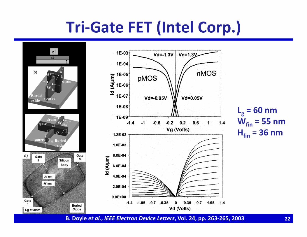
Tri‐Gate FET (Intel Corp.)
B. Doyle et al., IEEE Electron Device Letters, Vol. 24, pp. 263‐265, 2003 22
Lg = 60 nmWfin = 55 nmHfin = 36 nm
Bulk FinFET (Samsung Electronics)
C.‐H. Lee et al., Symposium on VLSI Technology Digest, pp. 130‐131, 2004
• FinFETs can be made on bulk‐Si waferslower costimproved thermal conduction
D. Ha, H. Takeuchi, Y.‐K. Choi, T.‐J. King, W. Bai, D.‐L. Kwong, A. Agarwal, and M. Ameen, “Molybdenum‐gate HfO2 CMOS FinFET technology,” IEEE International Electron Devices Meeting Technical Digest, pp. 643‐646, 2004
24
Impact of Fin Layout Orientation
(Series resistance is more significant at shorter Lg.)
• If the fin is oriented || or to the wafer flat, the channel surfaces lie along (110) planes.– Lower electron mobility– Higher hole mobility
• If the fin is oriented 45° to the wafer flat, the channel surfaces lie along (100) planes.
L. Chang et al. (IBM), SISPAD 2004
25
May 4, 2011: Intel Announcement
• Ivy Bridge‐based Intel® Core™ family processors will be the first high‐volume chips to use 3‐D Tri‐Gate transistors.
• This silicon technology breakthrough will also aid in the delivery of more highly integrated Intel® Atom™ processor‐based products…