International Journal of VLSI design & Communication Systems (VLSICS) Vol.2, No.4, December 2011 DOI : 10.5121/vlsic.2011.2415 179 Optimized Design of 2D Mesh NOC Router using Custom SRAM & Common Buffer Utilization Bhavana Pote 1 ,V. N. Nitnaware 2 ,and Dr. S. S. Limaye 3 1 Department of Electronics, Ramdeobaba Kamla Nehru College of Engg, Nagpur, India [email protected]2 Department of EDT, Ramdeobaba Kamla Nehru College of Engg, Nagpur, India [email protected]3 Jhulelal Institute of Technology, Nagpur, India [email protected]Abstract: With the shrinking technology, reduced scale and power-hungry chip IO leads to System on Chip. The design of SOC using traditional standard bus scheme encounters with issues like non-uniform delay androuting problems. Crossbars could scale better when compared to buses but tend to become huge with increasing number of nodes. NOC has become the design paradigm for SOC design for its highly regularized interconnect structure, good scalability and linear design effort. The main components of an NoC topology are the network adapters, routing nodes, and network interconnect links. This paper mainly deals with the implementation of full custom SRAM based arrays over D FF based register arrays in the design of input module of routing node in 2D mesh NOC topology. The custom SRAM blocks replace D FF(D flip flop) memory implementations to optimize area and power of the input block. Full custom design of SRAMs has been carried out by MILKYWAY, while physical implementation of the input module with SRAMs has been carried out by IC Compiler of SYNOPSYS.The improved design occupies approximately 30% of the area of the original design. This is in conformity to the ratio of the area of an SRAM cell to the area of a D flip flop, which is approximately 6:28.The power consumption is almost halved to 1.5 mW. Maximum operating frequency is improved from 50 MHz to 200 MHz. It is intended to study and quantify the behavior of the single pac ket array design in r elation to the multiple packet array design. Intuitively, a common packet buffer would result in better utilization of available buffer space. This in turn wouldtranslate into lower delays in transmission. A MATLAB model is used to show quantitatively how performance is improved in a common packet array design . Keywords : 2D mesh, virtual output queuing, HOL blocking, FIFO, DDC file, GDS format. 1. Introduction: A packet-switched 2- D mesh is the most used and st udied topology so far. It is also a sort of an average NOC currently. Good results and interesting proposals provoke design engineers to use this topology as the base [1] .The key research problems in the design of NOCs include but are not
Transcript
8/3/2019 Optimized Design of 2D Mesh NOC Router using Custom SRAM & Common Buffer Utilization
With the shrinking technology, reduced scale and power-hungry chip IO leads to System on Chip. The
design of SOC using traditional standard bus scheme encounters with issues like non-uniform delay and
routing problems. Crossbars could scale better when compared to buses but tend to become huge with
increasing number of nodes. NOC has become the design paradigm for SOC design for its highly
regularized interconnect structure, good scalability and linear design effort. The main components of an
NoC topology are the network adapters, routing nodes, and network interconnect links. This paper mainly
deals with the implementation of full custom SRAM based arrays over D FF based register arrays in the
design of input module of routing node in 2D mesh NOC topology. The custom SRAM blocks replace D
FF(D flip flop) memory implementations to optimize area and power of the input block. Full custom design
of SRAMs has been carried out by MILKYWAY, while physical implementation of the input module withSRAMs has been carried out by IC Compiler of SYNOPSYS.The improved design occupies approximately
30% of the area of the original design. This is in conformity to the ratio of the area of an SRAM cell to the
area of a D flip flop, which is approximately 6:28.The power consumption is almost halved to 1.5 mW.
Maximum operating frequency is improved from 50 MHz to 200 MHz. It is intended to study and quantify
the behavior of the single packet array design in relation to the multiple packet array design. Intuitively, a
common packet buffer would result in better utilization of available buffer space. This in turn would
translate into lower delays in transmission. A MATLAB model is used to show quantitatively how
performance is improved in a common packet array design.
A packet-switched 2-D mesh is the most used and studied topology so far. It is also a sort of anaverage NOC currently. Good results and interesting proposals provoke design engineers to use
this topology as the base[1] .The key research problems in the design of NOCs include but are not
8/3/2019 Optimized Design of 2D Mesh NOC Router using Custom SRAM & Common Buffer Utilization
International Journal of VLSI design & Communication Systems (VLSICS) Vol.2, No.4, December 2011
180
limited to topology, channel width, buffer size, floorplan, routing, switching, scheduling, and IP
mapping[2]. Additionally, [3]lists research issues to be application modeling and optimization,
NOC communication architecture analysis and optimization, NOC communication architecture
evaluation, and NOC design validation and synthesis.
The most important metrics for NOCs are application runtime, silicon area, power consumption,and latency. All these are to be minimized and usually appropriate trade-off is sought[4]. The
required silicon area is the most commonly reported value (77%) followed by latency (55%) and
maximum operating frequency (50%). The other metrics have lower occurrence[1].
In this regard, the current work is related to optimization of buffers in the router design so as toachieve lower silicon area, lower power and higher operating frequency.
The input block in the design of router consists of six major components: the packet array, the
linked list array, the destination head array, the destination tail array, the free-list FIFO, and a
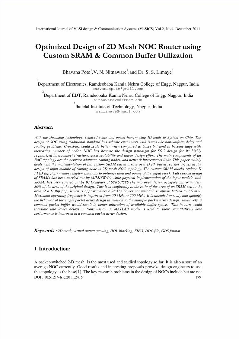
shift register, see fig. 3.1. Four of these six components are conventional memory elements. In astandard cell based design, memory elements are realized using D flip flops in the standard
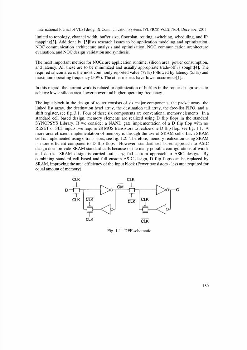
SYNOPSYS Library. If we consider a NAND gate implementation of a D flip flop with noRESET or SET inputs, we require 28 MOS transistors to realize one D flip flop, see fig. 1.1. A
more area efficient implementation of memory is through the use of SRAM cells. Each SRAM
cell is implemented using 6 transistors, see fig. 1.2. Therefore, memory realization using SRAMis more efficient compared to D flip flops. However, standard cell based approach to ASIC
design does provide SRAM standard cells because of the many possible configurations of width
and depth. SRAM design is carried out using full custom approach to ASIC design. By
combining standard cell based and full custom ASIC design, D flip flops can be replaced by
SRAM, improving the area efficiency of the input block (Fewer transistors - less area required forequal amount of memory).
Fig. 1.1 DFF schematic
8/3/2019 Optimized Design of 2D Mesh NOC Router using Custom SRAM & Common Buffer Utilization
International Journal of VLSI design & Communication Systems (VLSICS) Vol.2, No.4, December 2011
181
Fig. 1.2 SRAM schematic
The queues are maintained in a packet array. Queue size is dynamically determined dependingon the arrival pattern of the data. If more data is destined for output port “m”, then
correspondingly, more buffer space, and hence, a longer queue is maintained for data packets to
be routed to output port “m,” subject to the maximum space available in the packet array (Fig.1.3).
Fig. 1.3 Each input port has its own buffer
An alternative design is based on using a common packet for all the input ports. For example, if
the crossbar switch consists of four input ports, then the original design calls for four packet
arrays. The proposed design would utilize one common packet array for all the four input ports
(Fig.1.4)
8/3/2019 Optimized Design of 2D Mesh NOC Router using Custom SRAM & Common Buffer Utilization
International Journal of VLSI design & Communication Systems (VLSICS) Vol.2, No.4, December 2011
182
Fig. 1.4 Common buffer shared between all input ports
It is intended to study and quantify the behavior of the single packet array design in relation to the
multiple packet array design. Intuitively, a common packet buffer would result in better
utilization of available buffer space. This in turn would translate into lower delays in
transmission.
2. Introduction to A 2D Mesh NOC:
Fig. 2.1 : A 2D Mesh NOC structure
A NOC consists of routers/switch, links, and network interfaces (Fig. 2.1). Routers direct dataover several links (hops). Routers further consists of a scheduler, buffer to store the incoming
data packet and the crossbar. Topology defines their logical lay-out (connections) whereas floor
plan defines the physical layout. The function of a network interface (adapter) is to decouple
computation (the resources) from communication (the network). Routing decides the path taken
from source to the destination whereas switching and flow control policies define the timing of transfers[2][5]. Task scheduling refers to the order in which the application tasks are executed
and task mapping defines which processing element (PE) executes certain task. IP mapping, on
the other hand, defines how PEs and other resources are connected to the NoC.
For illustrative purposes, Fig. 2.1 shows an example SOC with a NOC and nine heterogeneous IPblocks that are CPUs, memories, input/output devices, and HW accelerators.
2.1 Router Structure
NOC architectures are based on packet-switched networks, see figure 2.2a. This has led to new
and efficient principles for design of routers for NOC[6]. Assume that a router for the mesh
topology has four inputs and four outputs from/to other routers, and another input and output
from/to the Network Interface (NI). Routers can implement various functionalities - from simple
switching to intelligent routing. Since embedded systems are constrained in area and power
consumption, but still need high data rates, routers must be designed with hardware usage in
mind. For circuit-switched networks, routers may be designed with no queuing (buffering). For
packet-switched networks, some amount of buffering is needed, to support bursty data transfers.
8/3/2019 Optimized Design of 2D Mesh NOC Router using Custom SRAM & Common Buffer Utilization
International Journal of VLSI design & Communication Systems (VLSICS) Vol.2, No.4, December 2011
183
Such data originate in multimedia applications such as video streaming. Buffers can be provided
at the input, at the output, or at both input and output [7].
Various designs and implementations of router architectures based on different routing strategies
have been proposed in the literature. Wolkotte et al. proposed a circuit switched router
architecture for NOC[8], while Dally and Towles proposed a packet switched router architecture[9]. Albenes and Frederico provided a wormhole-based packet forwarding design for a NOC
switch[10].
Fig 2.2 (a) NOC Router (b) Router Components In this paper, the buffers in the design of the routers are based on the principle of virtual output
queuing since it is simple and reduces the risk of Head of Line Blocking[11] [12] [13].
In this paper, the scheduling policy embodied in the router is based on Iterative SLIP algorithm.
iSLIP uses round-robin to choose on port among those contending. This permits simpler hardware
implementations compared, besides making iSLIP faster. iSLIP achieves close to maximal
matches after just one or two iterations.. iSLIP achieves 100% throughput under uniform trafficand the round robin policy ensures fairness among contenders.
Even though its behavior may be unstable under bursty traffic, iSLIP is commonly implemented
in commercial switches due to its simplicity[14]. This algorithm becomes more silicon area
efficient if it is implemented with its folding concept[15].
3. Implementation of input module with D FF based array vs CUSTOM
SRAM.
The traditional design of input module consists of D FFs based register arrays[16], see fig. 3.1
The same function of input module we intended to achieve using full custom SRAM replacing the
register arrays. The input module with arrays based on D FFs is now replaced by the input
module with full custom SRAMs, see fig.3.2
The input block is synthesized using the Synopsys 90 nm EDK standard cell library. Memoryelements are synthesized using D flip flops using the standard cell library. In order to save silicon
area, D flip flop memory is replaced by custom built SRAM. The SRAM provided by Synopsys
in the 90 nm process are available in sizes (width x depth) of 8x16, 8x32, and 128x64.
8/3/2019 Optimized Design of 2D Mesh NOC Router using Custom SRAM & Common Buffer Utilization
International Journal of VLSI design & Communication Systems (VLSICS) Vol.2, No.4, December 2011
184
However, the input block requires packet array memory of size 72x32. This is realized using
SRAM of size 128x64. The free-list FIFO requires a 6x32 memory. This is implemented using
an SRAM of 8x32. The destination head and destination tail arrays are of size 6x8. These are
replaced by SRAM of size 8x16. The SRAM used is underutilized. However, due to more
compact implementation, overall design area is greatly reduced, as shown by results in the
following section.
Fig.3.1 Input module with D FF based register arrays [17]
Custom SRAM IP is generated by full custom mask layout. Synopsys provides SRAM macros in
LEF format. In order to integrate SRAM into the input block, this LEF file is used to generate
CEL, FRAM, and LM views. Synopsys Milkyway is used to process the LEF file to create CEL,
FRAM, and LM views. These views combine to produce a reference library for IC Compiler.
The layout of the input block using SRAM requires CEL, FRAM, and LM views of the 90nmstandard library as well as the SRAM macro. The design file containing the input block gate
level netlist is a DDC file. This file is generated by Design Compiler from RTL code by applying
appropriate constraints.
8/3/2019 Optimized Design of 2D Mesh NOC Router using Custom SRAM & Common Buffer Utilization
International Journal of VLSI design & Communication Systems (VLSICS) Vol.2, No.4, December 2011
190
The input block optimized for area and power by incorporation of custom SRAM blocks into the
design. The custom SRAM blocks replace DFF(D flip flop) memory implementations. The
amount of hardware resources required to store one bit of information using and SRAM cell (6
transistors) is much less than the hardware requirements for storing one bit of information using
DFF (28 transistors).
The use of SRAM macros in place of standard cell D flip flops have resulted in an area reduction
and corresponding reduction in power consumption. The improved design occupies
approximately 30% of the area of the original design. This is in conformity to the ratio of the
area of an SRAM cell to the area of a D flip flop, which is approximately 6:28. The power
consumption is almost halved to 1.5 mW. Maximum operating frequency is improved from 50Mhz to 200 Mhz.
The utilization efficiency of the packet buffer array improves when a common buffer is used
instead of individual buffers in each input port. This is manifested in the form of lower delay in transferring a packet from the input to the output. The delay is improved by approximately 40%through the use of a common buffer.
REFERENCES :
[1] Salminen et al., survey of network-on-chip proposals, white paper, @ OCP-IP, march 2008.
[2] U. Ogras, J. Hu, and R. Marculescu, “Key Research Problems in NoC Design: A Holisitic
Perspective,” in Proceedings of the CODES, ISSS, 2005, pp. 69-74.
[3] R. Marculescu, U. Ogras, L. Peh, N. Jerger, and Y. Hoskote, “Outstanding Research Problems in
NoC Design: System, Microarchitecture, and Circuit Perspectives,” IEEE Transactions on Computer
Aided Design of Integrated Circuits and Systems, Vol. 28, No. 1, January 2009.
[4] E. Salminen, A. Kulmala, and T. H¨am¨al¨ainen, “On network-on-chip comparison,” in Euromicro
DSD, Aug. 2007, pp. 503–510
[5] S. Lee, “Implementation of a NoC”, KAIST, 2005.
[6] E . Rijpkema, K. Goossens, A. Radulescu, J. Dielissen, J. van Meerbergen, P.Wielage, and E.
Waterlander,“Trade-offs in the design of a router with both guaranteed and best-effort services for
networks on chip”, IEE Proc. on Computers and Digital Techniques, vol. 150, Issue 5, pp. 294-302,
September 2003.
[7] A. Kumar, D. Manjunath, and J. Kuri, Communication Networking: An Analytical Approach,
Morgan Kaufmann, 2004.
[8] P. T. Wolkotte, G. J. M. Smit, G. K. Rauwerda, and L. T. Smit, “An energy-efficient reconfigurable
circuit- switched network-on-chip”, Proc. 19th IEEE International Conference on Parallel andDistributed Processing Symposium, pp. 155-163, 2005.
[9] J. W. Dally and B. Towles, “Route packets, not wires: On-Chip interconnection networks”, Proc.
IEEE International Conference on Design and Automation, pp.684-689, June 2001.
[10] C. Albenes, Zeferino Frederico G. M. E. Santo, Altarniro Amadeu Susin, “ParlS: A parameterizable
interconnect switch for Networks-on-Chips”, Proc. ACM Conference, pp. 204-209, 2004.
8/3/2019 Optimized Design of 2D Mesh NOC Router using Custom SRAM & Common Buffer Utilization