22
1 Design and Simulation of RF CMOS Oscillators in Advanced Design System (ADS) By Amir Ebrahimi School of Electrical and Electronic Engineering The University of Adelaide June 2014
| Date post: | 07-Aug-2018 |
| Category: |
Documents |
| Upload: | meenakshi-sundaram |
| View: | 223 times |
| Download: | 0 times |
8/20/2019 Oscillator Ads
http://slidepdf.com/reader/full/oscillator-ads 1/22
1
Design and Simulation of RF CMOS
Oscillators in Advanced Design
System (ADS)
By
Amir Ebrahimi
School of Electrical and Electronic Engineering
The University of Adelaide
June 2014
8/20/2019 Oscillator Ads
http://slidepdf.com/reader/full/oscillator-ads 2/22
2
Contents
1- Introduction.................................................................................................... 3
1-1-
Objectives............................................................................................... 3
2- Ring Oscillators............................................................................................... 4
2-1- Oscillator Design..................................................................................... 5
2-1-1- DC Simulation of Gain stages............................................................ 6
2-1-2- AC Simulation of Gain stages............................................................ 10
2-1-3- Transient Simulation of the Complete Oscillator Circuit........................ 13
2-1-4- Harmonic Balance Simulation of the Complete Oscillator Circuit............ 16
2-1-4-1- Oscillator Output Voltage Spectrum............................................ 16
2-1-4-2- Oscillator Phase Noise.............................................................. 18
References.......................................................................................................... 22
8/20/2019 Oscillator Ads
http://slidepdf.com/reader/full/oscillator-ads 3/22
3
1- Introduction
This tutorial is a quick guide for new ADS users to design CMOS RF oscillators and do the
post processing on their simulation data in ADS.
Oscillators are fundamental parts of any RF communication systems. They are used as clockgenerators in microprocessors, local oscillators (LOs) for up/down conversion of the
information bearing signal and carrier signal generators for modulations. Robust and high
performance design of oscillators in CMOS technology poses interesting challenges.
Here, the design and simulation of CMOS ring oscillator in ADS will be presented and the
simulation procedures for obtaining the different output parameters like: transient output
waveform, output spectrum and phase noise are explained.
1-1- Objectives:
Design a 3-stage ring oscillator based on common-source gain stages
Performing the DC simulation for setting the gain stages DC bias point
Performing the AC simulation for finding the individual and loop gain of the oscillator
Performing transient analysis for displaying the oscillator output waveform in time
domain
Performing the “Harmonic Balance” simulation for finding the output spectrum in
frequency domain
Using “Harmonic Balance” simulation for “Phase Noise” analysis of the oscillator
8/20/2019 Oscillator Ads
http://slidepdf.com/reader/full/oscillator-ads 4/22
4
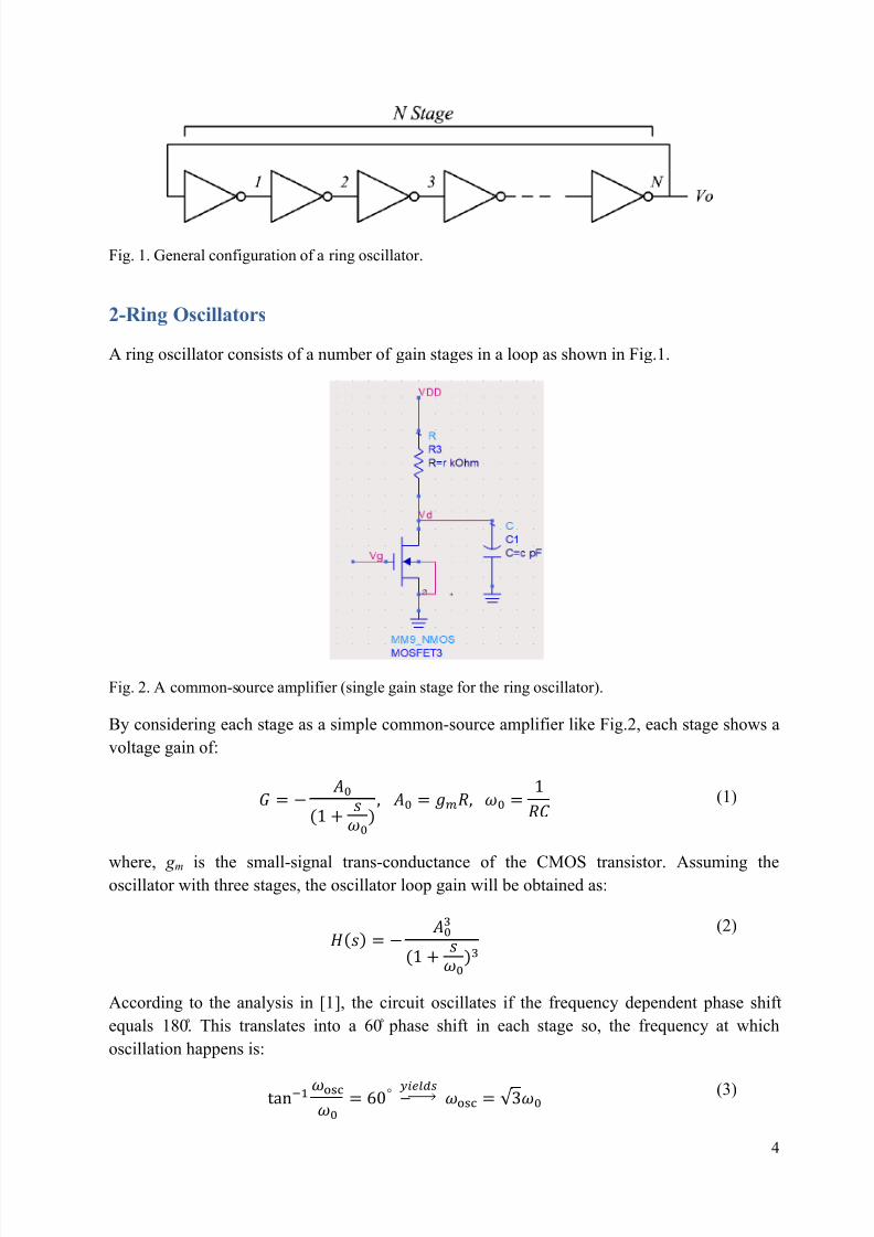
Fig. 1. General configuration of a ring oscillator.
2-Ring Oscillators
A ring oscillator consists of a number of gain stages in a loop as shown in Fig.1.
Fig. 2. A common-source amplifier (single gain stage for the ring oscillator).
By considering each stage as a simple common-source amplifier like Fig.2, each stage shows a
voltage gain of:
(1)
where, g m is the small-signal trans-conductance of the CMOS transistor. Assuming theoscillator with three stages, the oscillator loop gain will be obtained as:
(2)
According to the analysis in [1 the circuit oscillates if the frequency dependent phase shift
equals This translates into a phase shift in each stage so, the frequency at which
oscillation happens is:
(3)
8/20/2019 Oscillator Ads
http://slidepdf.com/reader/full/oscillator-ads 5/22
5
On the other hand, for oscillation, the minimum voltage gain per stage must be such that the
magnitude of the loop gain at ωosc is unity.
(4)
In circuit designs the gain should be chosen slightly larger than 2.
2-1- Oscillator Design
In order to design the oscillator loop, firstly, a single gain stage of Fig. 2 should be designed. It
can be designed based on the following steps:
S. 1- It is known that in oscillation mode, the source and drain terminals of all three transistors
will take the same DC voltage [2] so, for each gain stage we have:
(4)
S. 2- By considering the above condition, for a single gain stage of Fig. 2 in DC condition we
have:
(5)
S. 3- Based on the loop gain analysis (4), we assume A0 = 2.5.
(6)
S. 4- By substituting (6) into (5), the following relation is obtained giving us the appropriate
value of V G(DC) for designing a single gain stage.
(7)
S. 5- By calculating V G, the value of drain resistor ( R) can be calculated from (6).
S. 6- Finally, the capacitor (C ) value can be calculated by considering the ωosc and (3).
Now, suppose that a ring oscillator of three common-source gain stages has to be designed for
the oscillation frequency of 1 GHz with V DD = 5 V. The considered transistor size is ( ) in 0.5 µm standard CMOS technology with the parameters given in [1], which are
listed in Table 1.
8/20/2019 Oscillator Ads
http://slidepdf.com/reader/full/oscillator-ads 6/22
6
Table 1: Level 1 SPICE Models for NMOS and PMOS Devices in 0.5 µm CMOC Technology.
NMOS Model
Level=1 VTO=0.7 GAMMA=0.45 PHI=0.9
NSUB=9e+14 LD=0.08e-6 UO=350 LAMBDA=0.1
TOX=9e-9 PB=0.9 CJ=0.56e-3 CJSW=0.35e-11
MJ=0.45 MJSW=0.2 CGDO=0.4e-9 JS=1.0e-8
PMOS Model
Level=1 VTO=-0.8 GAMMA=0.4 PHI=0.8
NSUB=5e+14 LD=0.09e-6 UO=100 LAMBDA=0.2
TOX=9e-9 PB=0.9 CJ=0.94e-3 CJSW=0.32e-11
MJ=0.5 MJSW=0.3 CGDO=0.3e-9 JS=0.5e-8
Based on the (S. 1- S. 6) and the data given in Table 1, the calculated values of V G(DC), R and C
are 3 V 2 kΩ and 29 pF respectively
2-1-1- DC Simulation of Gain stages
For starting create a new “Workspace” in ADS as shown below and name it “RingOsc” .
Fig. 3. Creating a new workspace in ADS.
8/20/2019 Oscillator Ads
http://slidepdf.com/reader/full/oscillator-ads 7/22
7
After creating the new workspace, open a new schematic window as shown in Fig. 4 and name
it “DCSim”.
Fig. 4. Creating a new schematic window.
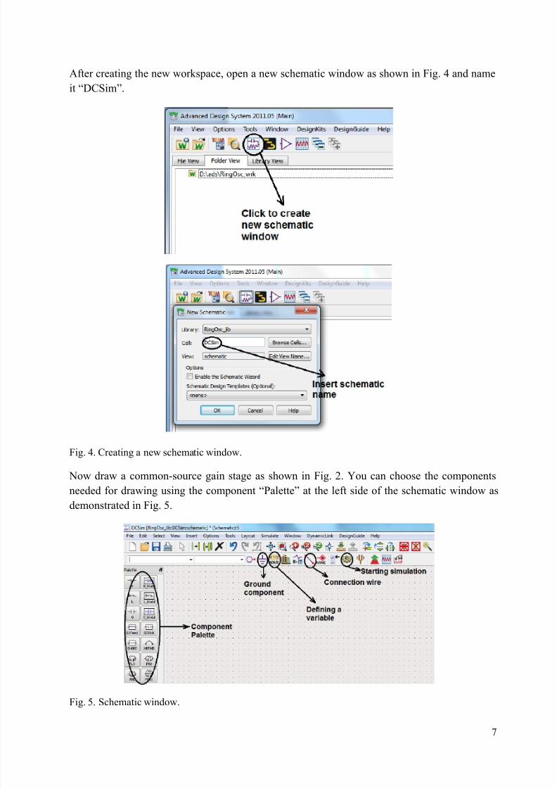
Now draw a common-source gain stage as shown in Fig. 2. You can choose the components
needed for drawing using the component “Palette” at the left side of the schematic window as
demonstrated in Fig. 5.
Fig. 5. Schematic window.
8/20/2019 Oscillator Ads
http://slidepdf.com/reader/full/oscillator-ads 8/22
8
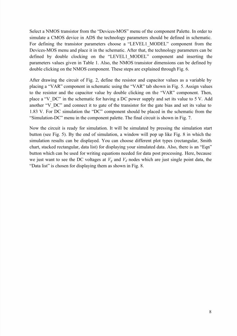
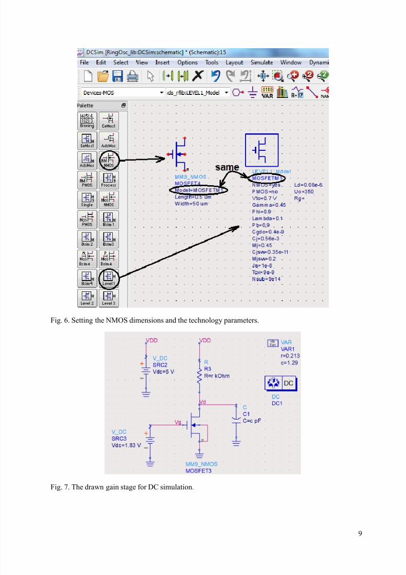
Select a NMOS transistor from the “Devices-MOS” menu of the component Palette In or der to
simulate a CMOS device in ADS the technology parameters should be defined in schematic.
For defining the transistor parameters choose a “LEVEL_MODEL” component from the
Devices-MOS menu and place it in the schematic. After that, the technology parameters can be
defined by double clocking on the “LEVEL_MODEL” component and inserting the parameters values given in Table 1. Also, the NMOS transistor dimensions can be defined by
double clicking on the NMOS component. These steps are explained through Fig. 6.
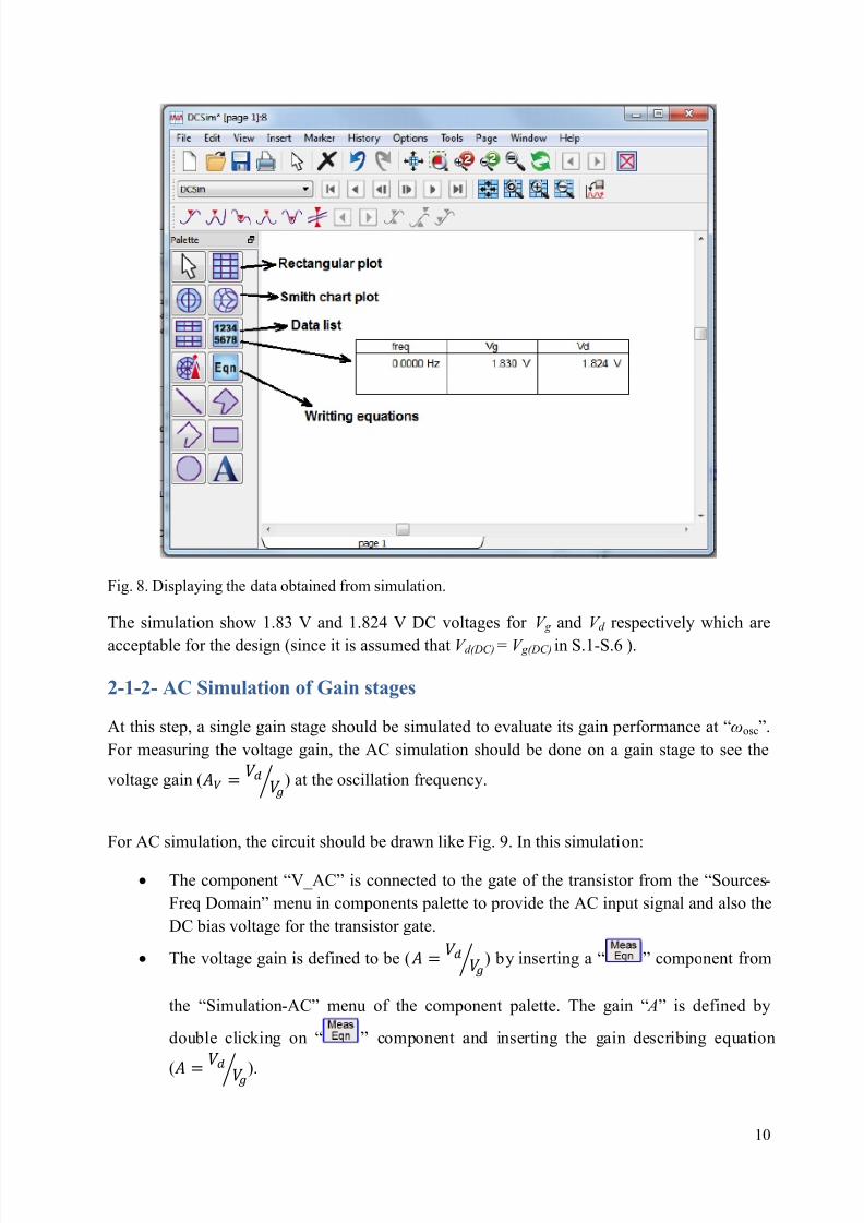
After drawing the circuit of Fig. 2, define the resistor and capacitor values as a variable by
placing a “VAR” component in schematic using the “VAR” tab shown in Fig 5 Assign values
to the resistor and the capacitor value by double clicking on the “VAR” component Then
place a “V_DC” in the schematic for having a DC power supply and set its value to 5 V Add
another “V_DC” and connect it to gate of the transistor for the gate bias and set its value to
1.83 V. For DC simulation the “DC” component should be placed in the schematic from the
“Simulation-DC” menu in the component palette The final circuit is shown in Fig 7
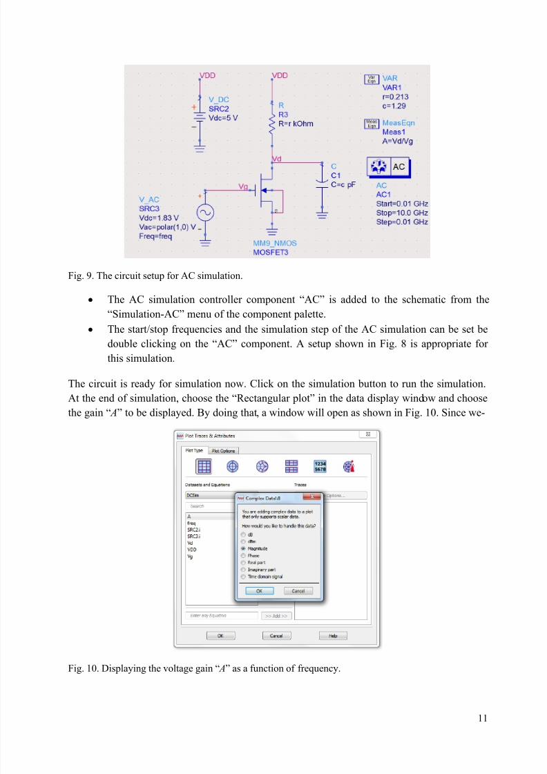
Now the circuit is ready for simulation. It will be simulated by pressing the simulation start
button (see Fig. 5). By the end of simulation, a window will pop up like Fig. 8 in which the
simulation results can be displayed. You can choose different plot types (rectangular, Smith
chart, stacked rectangular, data list) for displaying your simulated data Also there is an “Eqn”
button which can be used for writing equations needed for data post processing. Here, because
we just want to see the DC voltages at V g and V d nodes which are just single point data, the
“Data list” is chosen for displaying them as shown in Fig
8/20/2019 Oscillator Ads
http://slidepdf.com/reader/full/oscillator-ads 9/22
9
Fig. 6. Setting the NMOS dimensions and the technology parameters.
Fig. 7. The drawn gain stage for DC simulation.
8/20/2019 Oscillator Ads
http://slidepdf.com/reader/full/oscillator-ads 10/22
10
Fig. 8. Displaying the data obtained from simulation.
The simulation show 1.83 V and 1.824 V DC voltages for V g and V d respectively which are
acceptable for the design (since it is assumed that V d(DC) = V g(DC) in S.1-S.6 ).
2-1-2- AC Simulation of Gain stages
At this step, a single gain stage should be simulated to evaluate its gain performance at “ωosc”.
For measuring the voltage gain, the AC simulation should be done on a gain stage to see the
voltage gain ( ) at the oscillation frequency.
For AC simulation, the circuit should be drawn like Fig. 9. In this simulation:
The component “V_AC” is connected to the gate of the transistor from the “Sources-
Freq Domain” menu in components palette to provide the AC input signal and also the
DC bias voltage for the transistor gate.
The voltage gain is defined to be ( ) by inserting a “ ” component from
the “Simulation-AC” menu of the component palette The gain “ A” is defined by
double clicking on “ ” component and inserting the gain describing equation
( ).
8/20/2019 Oscillator Ads
http://slidepdf.com/reader/full/oscillator-ads 11/22
11
Fig. 9. The circuit setup for AC simulation.
The AC simulation controller component “AC” is added to the schematic from the
“Simulation-AC” menu of the component palette
The start/stop frequencies and the simulation step of the AC simulation can be set be
double clicking on the “AC” component A setup shown in Fig is appropriate for
this simulation.
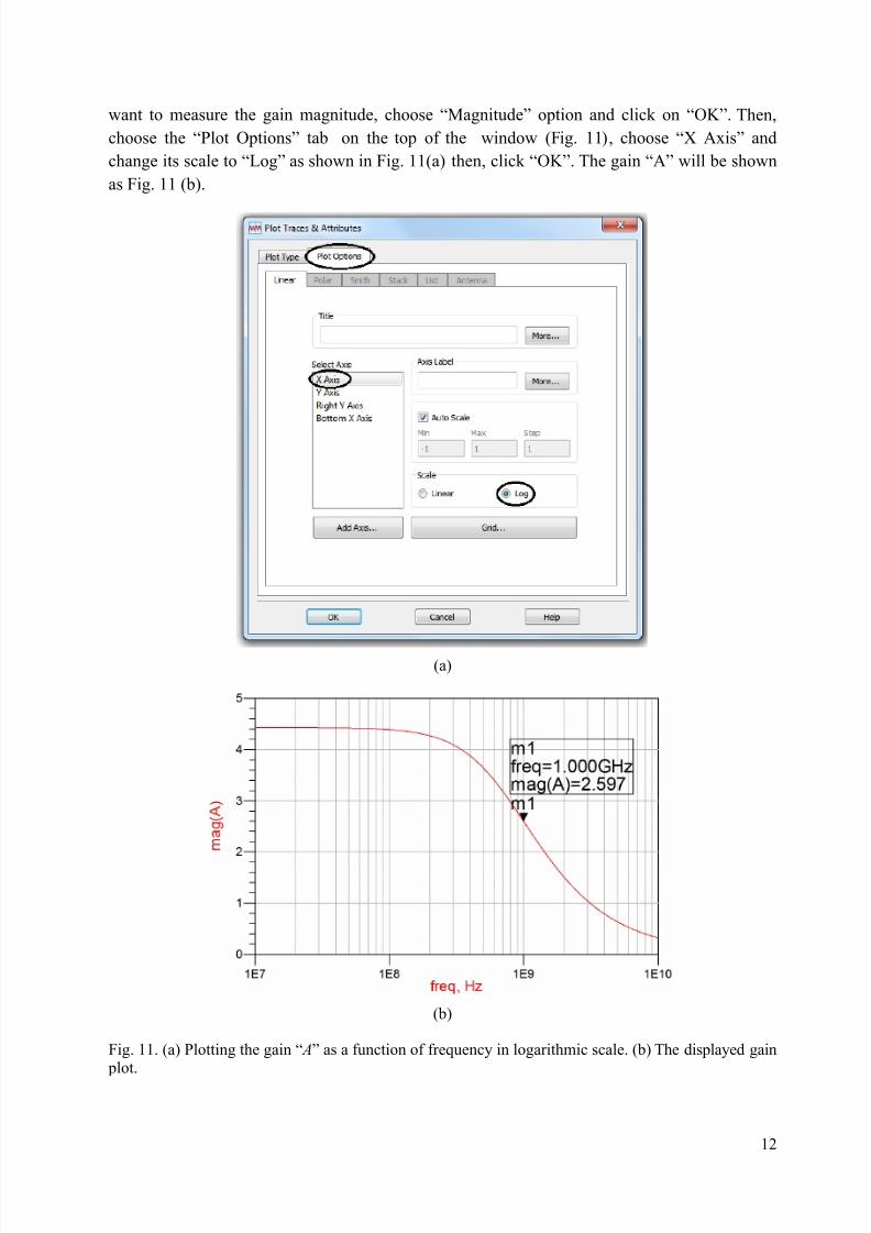
The circuit is ready for simulation now. Click on the simulation button to run the simulation.
At the end of simulation choose the “Rectangular plot” in the data display window and choose
the gain “ A” to be displayed By doing that, a window will open as shown in Fig. 10. Since we-
Fig Displaying the voltage gain “ A” as a function of frequency
8/20/2019 Oscillator Ads
http://slidepdf.com/reader/full/oscillator-ads 12/22
12
want to measure the gain magnitude choose “Magnitude” option and click on “OK” Then,
choose the “Plot Options” tab on the top of the window (Fig. 11) choose “X Axis” and
change its scale to “Log” as shown in Fig. 11(a) then click “OK” The gain “A” will be shown
as Fig. 11 (b).
(a)
(b)
Fig (a) Plotting the gain “ A” as a function of frequency in logarithmic scale (b) The displayed gain plot.
8/20/2019 Oscillator Ads
http://slidepdf.com/reader/full/oscillator-ads 13/22
13
Based on the gain plot in Fig. 11(b), the voltage gain at the considered oscillation frequency
“ f osc = GHz” is 259 which is in a good agreement with the assumption in (6).
If the simulated gain is smaller than 2 in AC simulation, the design procedure should be
repeated again with a larger value of “ R”
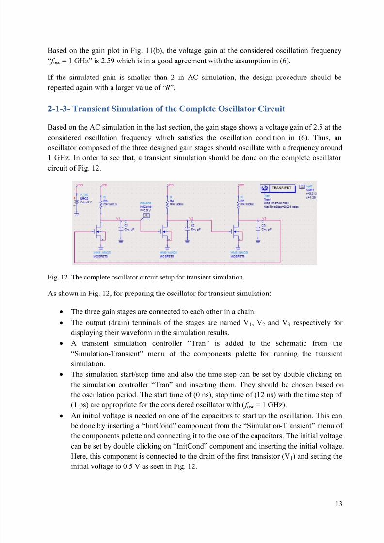
2-1-3- Transient Simulation of the Complete Oscillator Circuit
Based on the AC simulation in the last section, the gain stage shows a voltage gain of 2.5 at the
considered oscillation frequency which satisfies the oscillation condition in (6). Thus, an
oscillator composed of the three designed gain stages should oscillate with a frequency around
1 GHz. In order to see that, a transient simulation should be done on the complete oscillator
circuit of Fig. 12.
Fig. 12. The complete oscillator circuit setup for transient simulation.
As shown in Fig. 12, for preparing the oscillator for transient simulation:
The three gain stages are connected to each other in a chain.
The output (drain) terminals of the stages are named V1, V2 and V3 respectively for
displaying their waveform in the simulation results.
A transient simulation controller “Tran” is added to the schematic from the
“Simulation-Transient” menu of the components palette for running the transient
simulation.
The simulation start/stop time and also the time step can be set by double clicking on
the simulation controller “Tran” and inserting them They should be chosen based on
the oscillation period. The start time of (0 ns), stop time of (12 ns) with the time step of
(1 ps) are appropriate for the considered oscillator with ( f osc = 1 GHz).
An initial voltage is needed on one of the capacitors to start up the oscillation. This can
be done by inserting a “InitCond” component from the “Simulation-Transient” menu of
the components palette and connecting it to the one of the capacitors. The initial voltage
can be set by double clicking on “InitCond” component and inserting the initial voltage
Here, this component is connected to the drain of the first transistor (V1) and setting the
initial voltage to 0.5 V as seen in Fig. 12.
8/20/2019 Oscillator Ads
http://slidepdf.com/reader/full/oscillator-ads 14/22
14
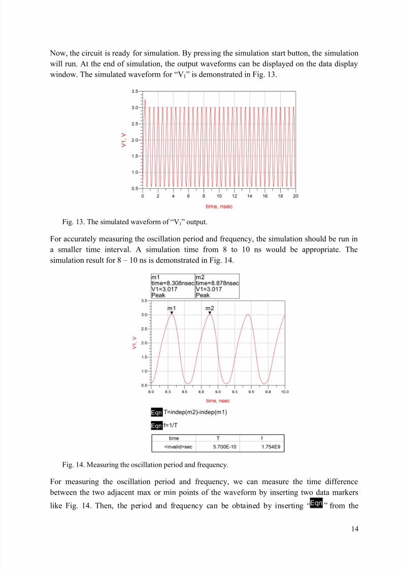
Now, the circuit is ready for simulation. By pressing the simulation start button, the simulation
will run. At the end of simulation, the output waveforms can be displayed on the data display
window. The simulated waveform for “V1” is demonstrated in Fig. 13.
Fig. 13. The simulated waveform of “V1” output
For accurately measuring the oscillation period and frequency, the simulation should be run in
a smaller time interval. A simulation time from 8 to 10 ns would be appropriate. The
simulation result for 8 – 10 ns is demonstrated in Fig. 14.
Fig. 14. Measuring the oscillation period and frequency.
For measuring the oscillation period and frequency, we can measure the time difference
between the two adjacent max or min points of the waveform by inserting two data markers
like Fig. 14. Then, the period and frequency can be obtained by inserting “ ” from the
8/20/2019 Oscillator Ads
http://slidepdf.com/reader/full/oscillator-ads 15/22
15
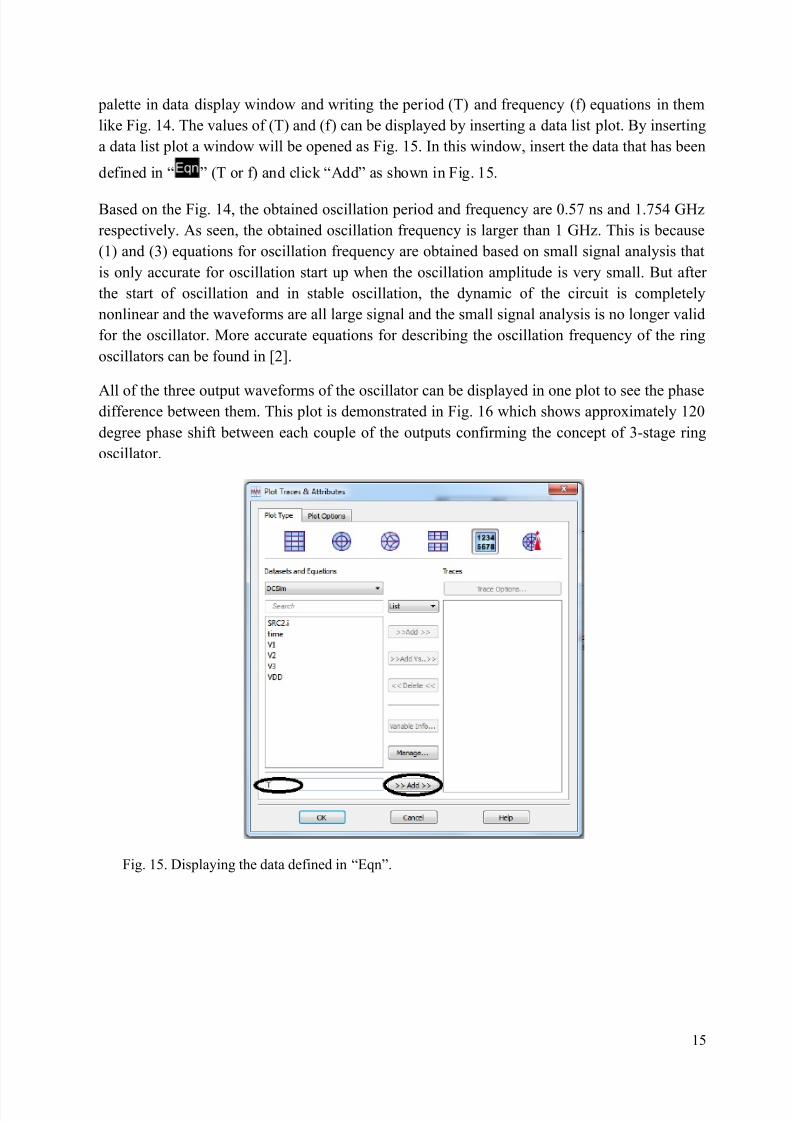
palette in data display window and writing the period (T) and frequency (f) equations in them
like Fig. 14. The values of (T) and (f) can be displayed by inserting a data list plot. By inserting
a data list plot a window will be opened as Fig. 15. In this window, insert the data that has been
defined in “ ” (T or f) and click “Add” as shown in Fig 5
Based on the Fig. 14, the obtained oscillation period and frequency are 0.57 ns and 1.754 GHz
respectively. As seen, the obtained oscillation frequency is larger than 1 GHz. This is because
(1) and (3) equations for oscillation frequency are obtained based on small signal analysis that
is only accurate for oscillation start up when the oscillation amplitude is very small. But after
the start of oscillation and in stable oscillation, the dynamic of the circuit is completely
nonlinear and the waveforms are all large signal and the small signal analysis is no longer valid
for the oscillator. More accurate equations for describing the oscillation frequency of the ring
oscillators can be found in [2].
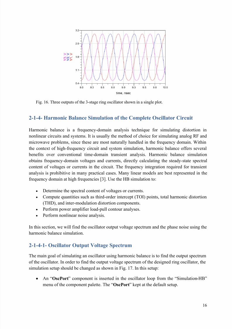
All of the three output waveforms of the oscillator can be displayed in one plot to see the phasedifference between them. This plot is demonstrated in Fig. 16 which shows approximately 120
degree phase shift between each couple of the outputs confirming the concept of 3-stage ring
oscillator.
Fig 5 Displaying the data defined in “Eqn”
8/20/2019 Oscillator Ads
http://slidepdf.com/reader/full/oscillator-ads 16/22
16
Fig. 16. Three outputs of the 3-stage ring oscillator shown in a single plot.
2-1-4- Harmonic Balance Simulation of the Complete Oscillator Circuit
Harmonic balance is a frequency-domain analysis technique for simulating distortion in
nonlinear circuits and systems. It is usually the method of choice for simulating analog RF and
microwave problems, since these are most naturally handled in the frequency domain. Within
the context of high-frequency circuit and system simulation, harmonic balance offers several
benefits over conventional time-domain transient analysis. Harmonic balance simulation
obtains frequency-domain voltages and currents, directly calculating the steady-state spectral
content of voltages or currents in the circuit. The frequency integration required for transient
analysis is prohibitive in many practical cases. Many linear models are best represented in thefrequency domain at high frequencies [3]. Use the HB simulation to:
Determine the spectral content of voltages or currents.
Compute quantities such as third-order intercept (TOI) points, total harmonic distortion
(THD), and inter-modulation distortion components.
Perform power amplifier load-pull contour analyses.
Perform nonlinear noise analysis.
In this section, we will find the oscillator output voltage spectrum and the phase noise using the
harmonic balance simulation.
2-1-4-1- Oscillator Output Voltage Spectrum
The main goal of simulating an oscillator using harmonic balance is to find the output spectrum
of the oscillator. In order to find the output voltage spectrum of the designed ring oscillator, the
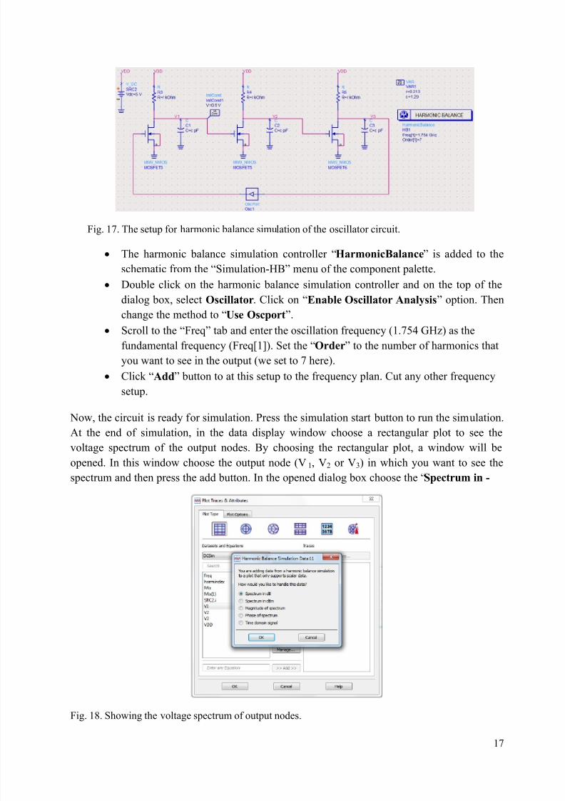
simulation setup should be changed as shown in Fig. 17. In this setup:
An “OscPort” component is inserted in the oscillator loop from the “Simulation -HB”
menu of the component palette. The “OscPort” kept at the default setup.
8/20/2019 Oscillator Ads
http://slidepdf.com/reader/full/oscillator-ads 17/22
17
Fig. 17. The setup for harmonic balance simulation of the oscillator circuit.
The harmonic balance simulation controller “HarmonicBalance” is added to the
schematic from the “Simulation-HB” menu of the component palette.
Double click on the harmonic balance simulation controller and on the top of the
dialog box, select Oscillator. Click on “Enable Oscillator Analysis” option Then
change the method to “Use Oscport”
Scroll to the “Freq” tab and enter the oscillation frequency (1.754 GHz) as the
fundamental frequency (Freq[) Set the “Order” to the number of harmonics that
you want to see in the output (we set to 7 here).
Click “Add” button to at this setup to the frequency plan Cut any other frequency
setup.
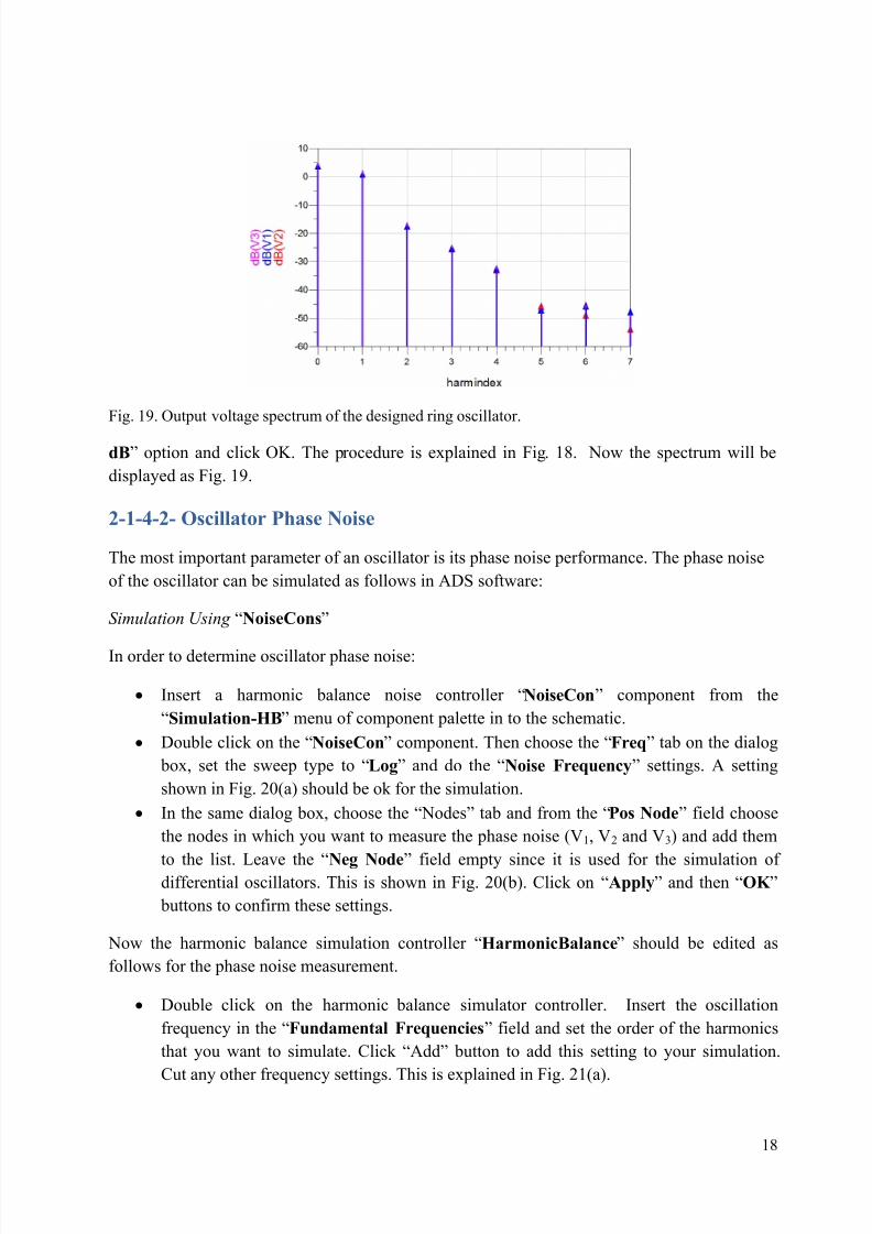
Now, the circuit is ready for simulation. Press the simulation start button to run the simulation.At the end of simulation, in the data display window choose a rectangular plot to see the
voltage spectrum of the output nodes. By choosing the rectangular plot, a window will be
opened. In this window choose the output node (V1, V2 or V3) in which you want to see the
spectrum and then press the add button In the opened dialog box choose the “Spectrum in -
Fig. 18. Showing the voltage spectrum of output nodes.
8/20/2019 Oscillator Ads
http://slidepdf.com/reader/full/oscillator-ads 18/22
18
Fig. 19. Output voltage spectrum of the designed ring oscillator.
dB” option and click OK. The procedure is explained in Fig. 18. Now the spectrum will be
displayed as Fig. 19.
2-1-4-2- Oscillator Phase Noise
The most important parameter of an oscillator is its phase noise performance. The phase noise
of the oscillator can be simulated as follows in ADS software:
Simulation Using “NoiseCons”
In order to determine oscillator phase noise:
Insert a harmonic balance noise controller “NoiseCon” component from the
“Simulation-HB” menu of component palette in to the schematic
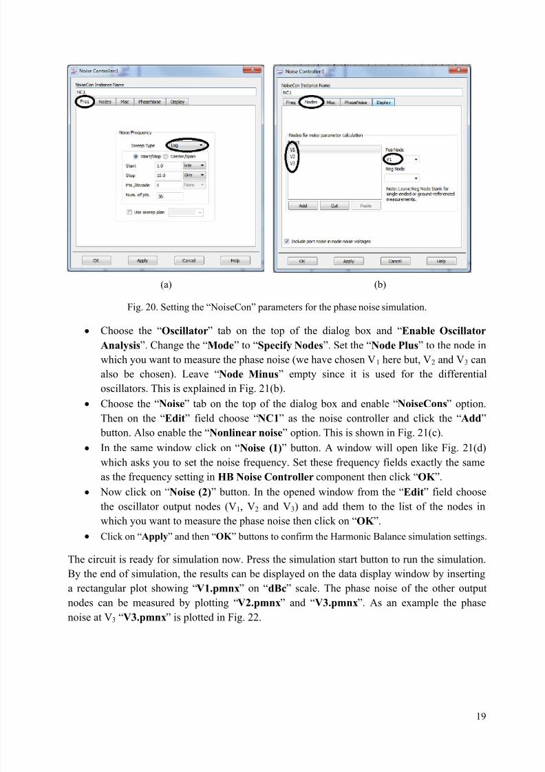
Double click on the “NoiseCon” component Then choose the “Freq” tab on the dialog
box set the sweep type to “Log” and do the “Noise Frequency” settings A setting
shown in Fig. 20(a) should be ok for the simulation.
In the same dialog box choose the “Nodes” tab and from the “Pos Node” field choose
the nodes in which you want to measure the phase noise (V1, V2 and V3) and add them
to the list Leave the “Neg Node” field empty since it is used for the simulation ofdifferential oscillators. This is shown in Fig. 20(b). Click on “Apply” and then “OK ”
buttons to confirm these settings.
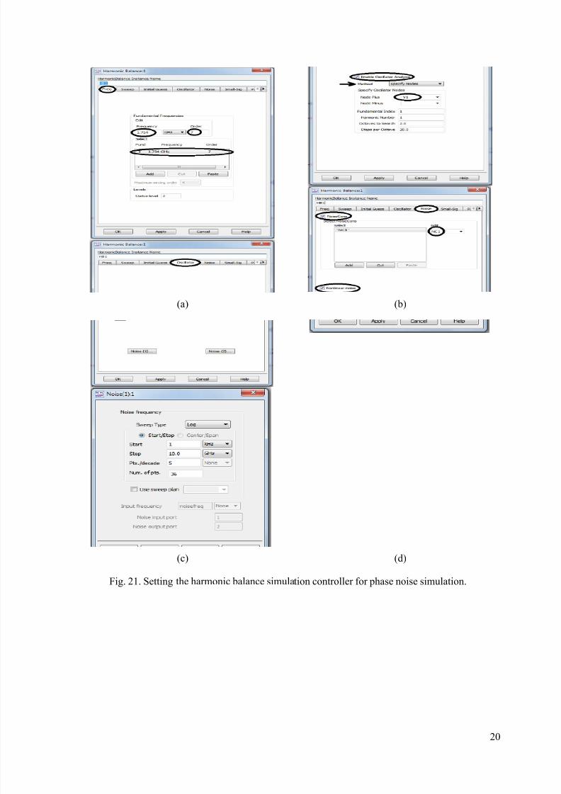
Now the harmonic balance simulation controller “HarmonicBalance” should be edited as
follows for the phase noise measurement.
Double click on the harmonic balance simulator controller. Insert the oscillation
frequency in the “Fundamental Frequencies” field and set the order of the harmonics
that you want to simulate Click “Add” button to add this setting to your simulation
Cut any other frequency settings. This is explained in Fig. 21(a).
8/20/2019 Oscillator Ads
http://slidepdf.com/reader/full/oscillator-ads 19/22
19
(a) (b)
Fig 2 Setting the “NoiseCon” parameters for the phase noise simulation.
Choose the “Oscillator” tab on the top of the dialog box and “Enable Oscillator
Analysis” Change the “Mode” to “Specify Nodes” Set the “Node Plus” to the node in
which you want to measure the phase noise (we have chosen V1 here but, V2 and V3 can
also be chosen) Leave “Node Minus” empty since it is used for the differential
oscillators. This is explained in Fig. 21(b).
Choose the “Noise” tab on the top of the dialog box and enable “NoiseCons” optionThen on the “Edit” field choose “NC1” as the noise controller and click the “Add”
button. Also enable the “Nonlinear noise” option This is shown in Fig. 21(c).
In the same window click on “Noise (1)” button A window will open like Fig 21(d)
which asks you to set the noise frequency. Set these frequency fields exactly the same
as the frequency setting in HB Noise Controller component then click “OK ”
Now click on “Noise (2)” button In the opened window from the “Edit” field choose
the oscillator output nodes (V1, V2 and V3) and add them to the list of the nodes in
which you want to measure the phase noise then click on “OK ”
Click on “Apply” and then “OK ” buttons to confirm the Harmonic Balance simulation settings
The circuit is ready for simulation now. Press the simulation start button to run the simulation.
By the end of simulation, the results can be displayed on the data display window by inserting
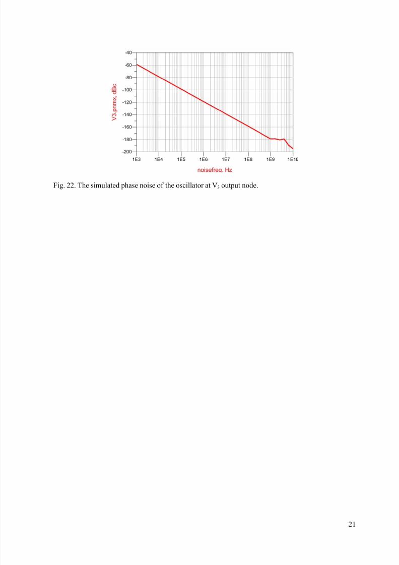
a rectangular plot showing “V1.pmnx” on “dBc” scale The phase noise of the other output
nodes can be measured by plotting “V2.pmnx” and “V3.pmnx” As an example the phase
noise at V3 “V3.pmnx” is plotted in Fig 22
8/20/2019 Oscillator Ads
http://slidepdf.com/reader/full/oscillator-ads 20/22
20
(a) (b)
(c) (d)
Fig. 21. Setting the harmonic balance simulation controller for phase noise simulation.
8/20/2019 Oscillator Ads
http://slidepdf.com/reader/full/oscillator-ads 21/22
21
Fig. 22. The simulated phase noise of the oscillator at V3 output node.
8/20/2019 Oscillator Ads
http://slidepdf.com/reader/full/oscillator-ads 22/22
22
References
[1] B. Razavi, Design of Analog CMOS Integrated Circuits, ch. 14, McGraw Hill, New
York, 2001.
[2] Farahabadi, P.M.; Miar-Naimi, H.; Ebrahimzadeh, A, "Closed-Form Analytical Equations
for Amplitude and Frequency of High-Frequency CMOS Ring Oscillators," IEEETransactions on Circuits and Systems I: Regular Papers, vol.56, no.12, pp.2669,2677,
Dec. 2009.
[3] http://eesof.tm.agilent.com/docs/adsdoc2004A/manuals.htm


