32
OU NanoLab/NSF NUE/Bumm & Johnson AFM Atomic Force Microscopy
| Date post: | 22-Dec-2015 |
| Category: |
Documents |
| Upload: | anthony-alexander |
| View: | 234 times |
| Download: | 2 times |
OU NanoLab/NSF NUE/Bumm & Johnson
AFMAtomic Force Microscopy

OU NanoLab/NSF NUE/Bumm & Johnson
Outline• Motivation• History• How the AFM works
– Two modes– Contact Mode– Non-Contact Mode– Force Measurements– Raster the Tip: Generating an Image– Scanning Sample
• OUr AFM– Pictures
• Examples– The Good– The Bad– And the Ugly
• Uses– Topographical Analysis– Thin Layer Depth– RMS Roughness Calculations
• Other types of Microscopy
OU NanoLab/NSF NUE/Bumm & Johnson
Motivation
• Digitally image a topographical surface• Determine the roughness of a surface sample or
to measure the thickness of a crystal growth layer
• Image non-conducting surfaces such as proteins and DNA
• Study the dynamic behavior of living and fixed cells
OU NanoLab/NSF NUE/Bumm & Johnson
History
• The Scanning Tunneling Microscope (STM) was invented by G. Binnig and H. Rohrer, for which they were awarded the Nobel Prize in 1984
• A few years later, the first Atomic Force Microscope (AFM) was developed by G. Binnig, Ch. Gerber, and C. Quate at Stanford University by gluing a tiny shard of diamond onto one end of a tiny strip of gold foil
• Currently AFM is the most common form of scanning probe microscopy
OU NanoLab/NSF NUE/Bumm & Johnson
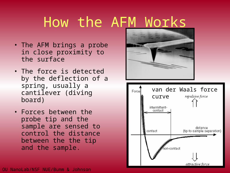
How the AFM Works
• The AFM brings a probe in close proximity to the surface
• The force is detected by the deflection of a spring, usually a cantilever (diving board)
• Forces between the probe tip and the sample are sensed to control the distance between the the tip and the sample.
van der Waals force curve
OU NanoLab/NSF NUE/Bumm & Johnson
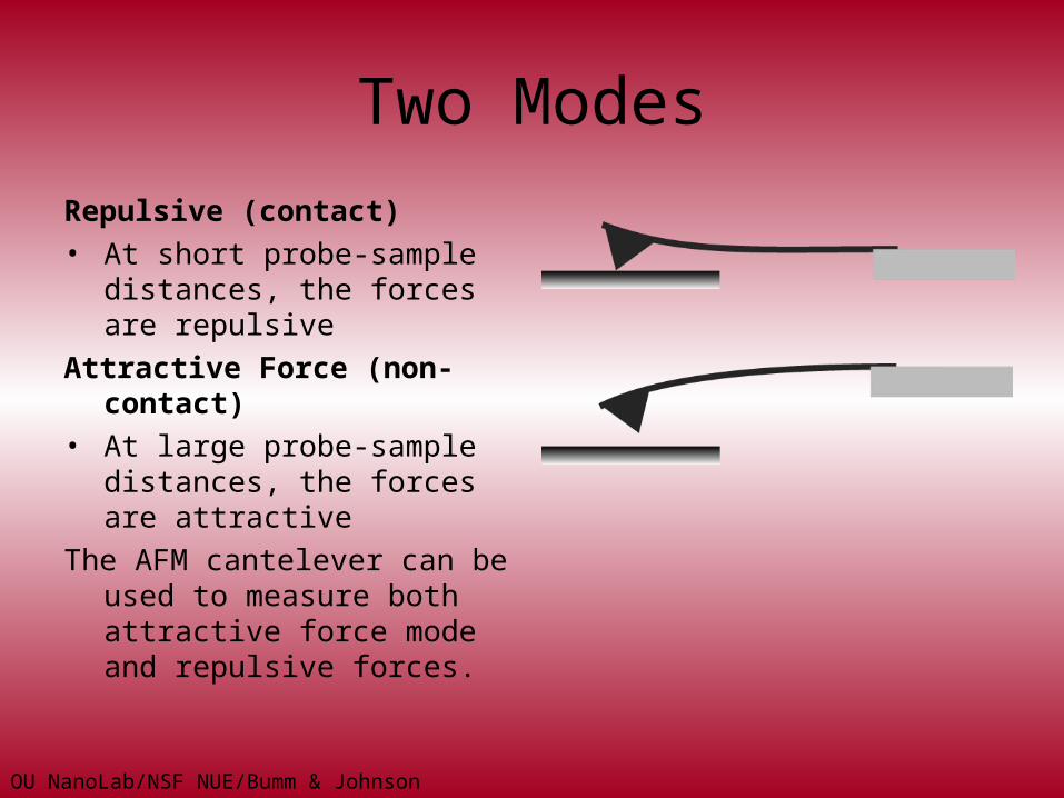
Two Modes
Repulsive (contact)• At short probe-sample
distances, the forces are repulsive
Attractive Force (non-contact)• At large probe-sample
distances, the forces are attractive
The AFM cantelever can be used to measure both attractive force mode and repulsive forces.
OU NanoLab/NSF NUE/Bumm & Johnson
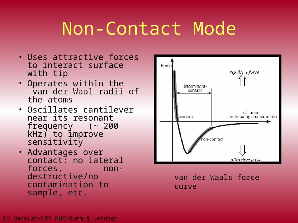
Non-Contact Mode
• Uses attractive forces to interact surface with tip
• Operates within the van der Waal radii of the atoms
• Oscillates cantilever near its resonant frequency (~ 200 kHz) to improve sensitivity
• Advantages over contact: no lateral forces, non-destructive/no contamination to sample, etc.
van der Waals force curve
OU NanoLab/NSF NUE/Bumm & Johnson
Contact Mode
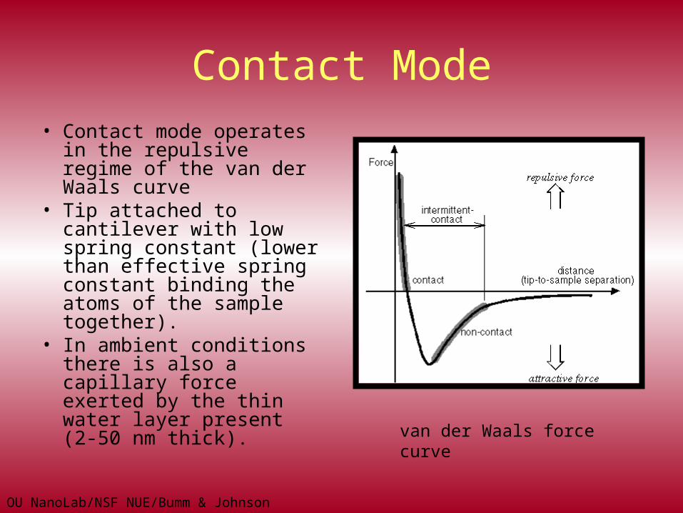
• Contact mode operates in the repulsive regime of the van der Waals curve
• Tip attached to cantilever with low spring constant (lower than effective spring constant binding the atoms of the sample together).
• In ambient conditions there is also a capillary force exerted by the thin water layer present (2-50 nm thick). van der Waals force curve
OU NanoLab/NSF NUE/Bumm & Johnson
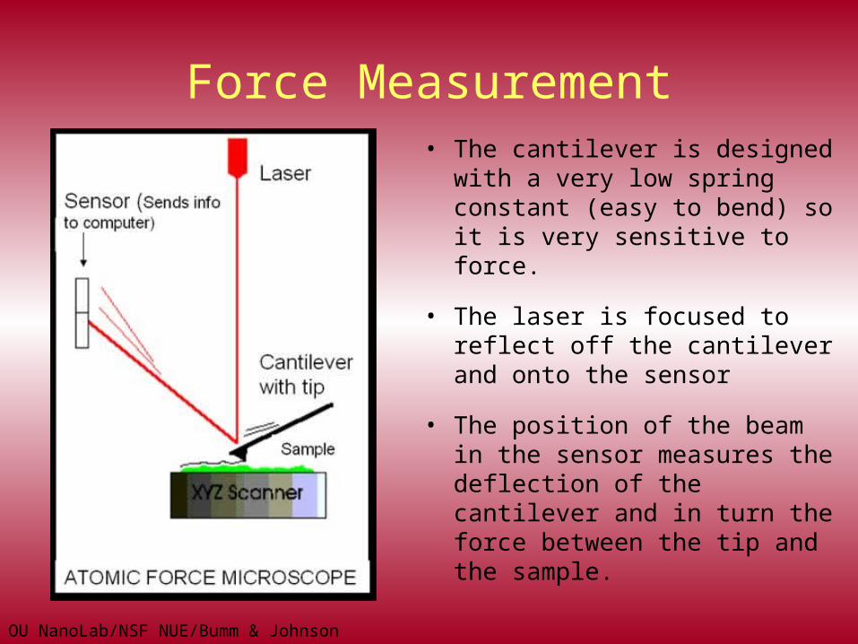
Force Measurement• The cantilever is designed with
a very low spring constant (easy to bend) so it is very sensitive to force.
• The laser is focused to reflect off the cantilever and onto the sensor
• The position of the beam in the sensor measures the deflection of the cantilever and in turn the force between the tip and the sample.
OU NanoLab/NSF NUE/Bumm & Johnson
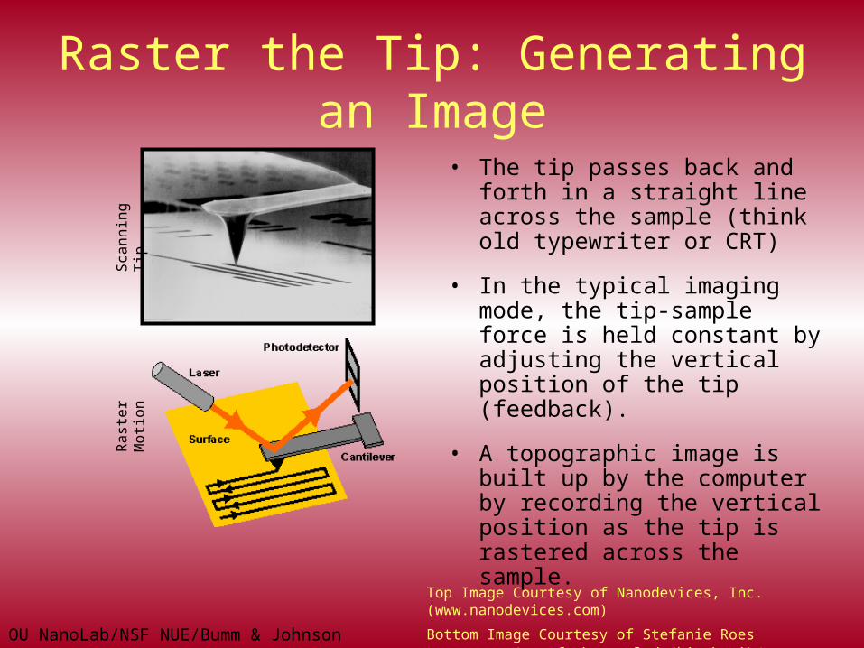
Raster the Tip: Generating an Image
• The tip passes back and forth in a straight line across the sample (think old typewriter or CRT)
• In the typical imaging mode, the tip-sample force is held constant by adjusting the vertical position of the tip (feedback).
• A topographic image is built up by the computer by recording the vertical position as the tip is rastered across the sample.
Sca
nn
ing
Tip
Ra
ste
r M
otio
n
Top Image Courtesy of Nanodevices, Inc. (www.nanodevices.com)
Bottom Image Courtesy of Stefanie Roes (www.fz-borstel.de/biophysik/ de/methods/afm.html)
OU NanoLab/NSF NUE/Bumm & Johnson
Scanning the Sample
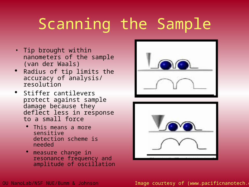
• Tip brought within nanometers of the sample (van der Waals)
Radius of tip limits the accuracy of analysis/ resolution
Stiffer cantilevers protect against sample damage because they deflect less in response to a small force This means a more sensitive
detection scheme is needed measure change in resonance
frequency and amplitude of oscillation
Image courtesy of (www.pacificnanotech.com)
OU NanoLab/NSF NUE/Bumm & Johnson
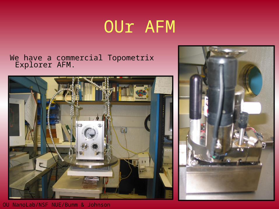
OUr AFM
We have a commercial Topometrix Explorer AFM.
OU NanoLab/NSF NUE/Bumm & Johnson
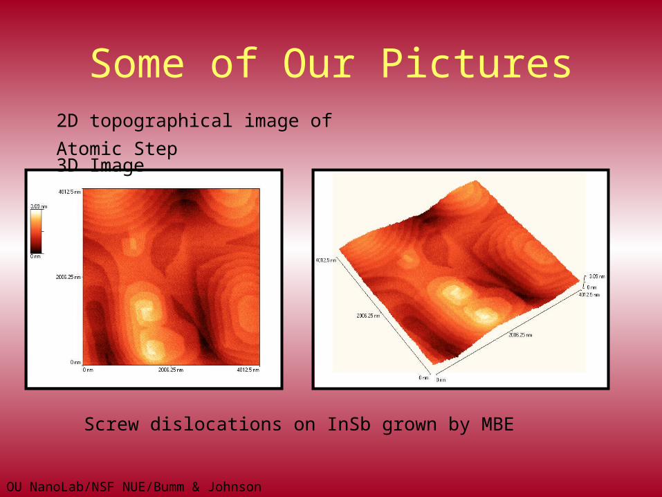
Some of Our Pictures2D topographical image of
Atomic Step 3D Image
Screw dislocations on InSb grown by MBE
OU NanoLab/NSF NUE/Bumm & Johnson
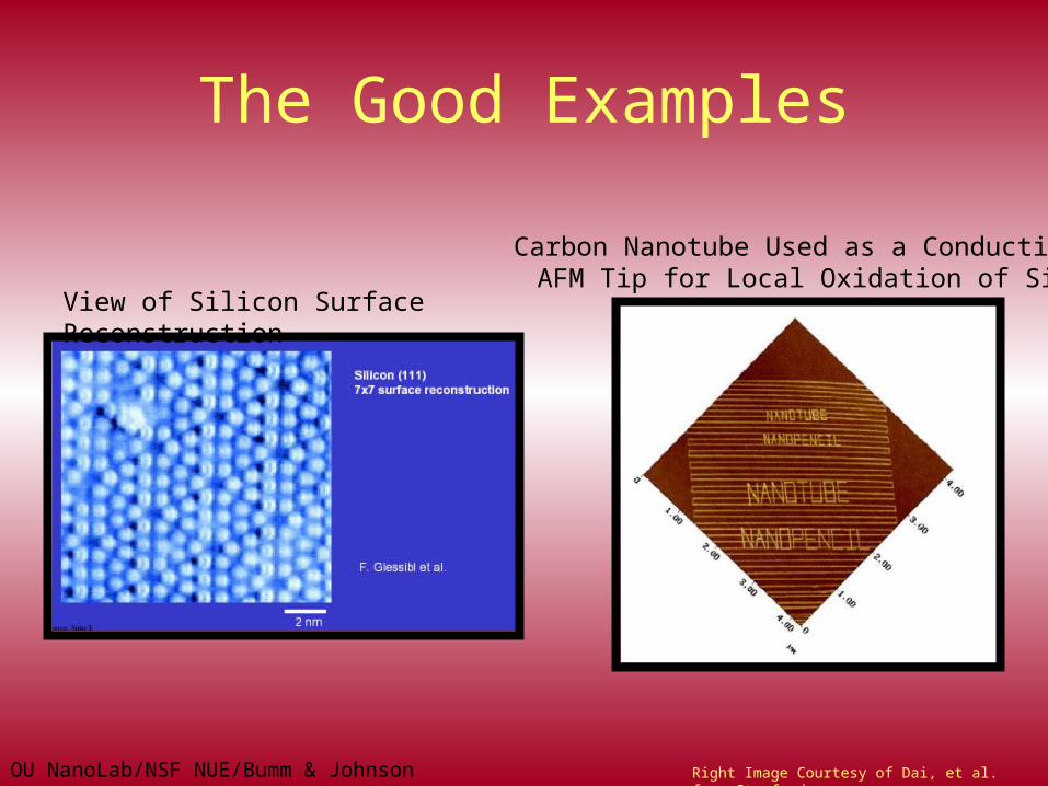
The Good Examples
View of Silicon Surface Reconstruction
Carbon Nanotube Used as a Conducting AFM Tip for Local Oxidation of Si.
Right Image Courtesy of Dai, et al. from Stanford
OU NanoLab/NSF NUE/Bumm & Johnson
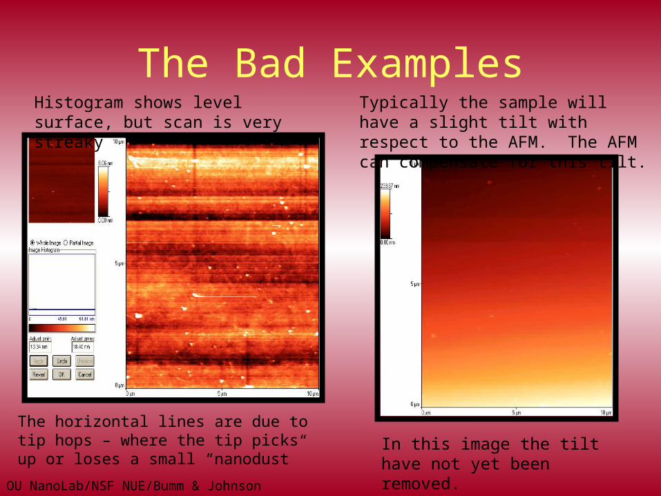
The Bad ExamplesHistogram shows level surface, but scan is very streaky
Typically the sample will have a slight tilt with respect to the AFM. The AFM can compensate for this tilt.
The horizontal lines are due to tip hops – where the tip picks up or loses a small “nanodust”
In this image the tilt have not yet been removed.

OU NanoLab/NSF NUE/Bumm & Johnson
And the Ugly!
Teeny little dust mites, ultra tiny dust mitesabout 2,000 in the average bed
Image courtesy of http://www.micropix.demon.co.uk/sem/dustmite/article/page_2.htm
OU NanoLab/NSF NUE/Bumm & Johnson
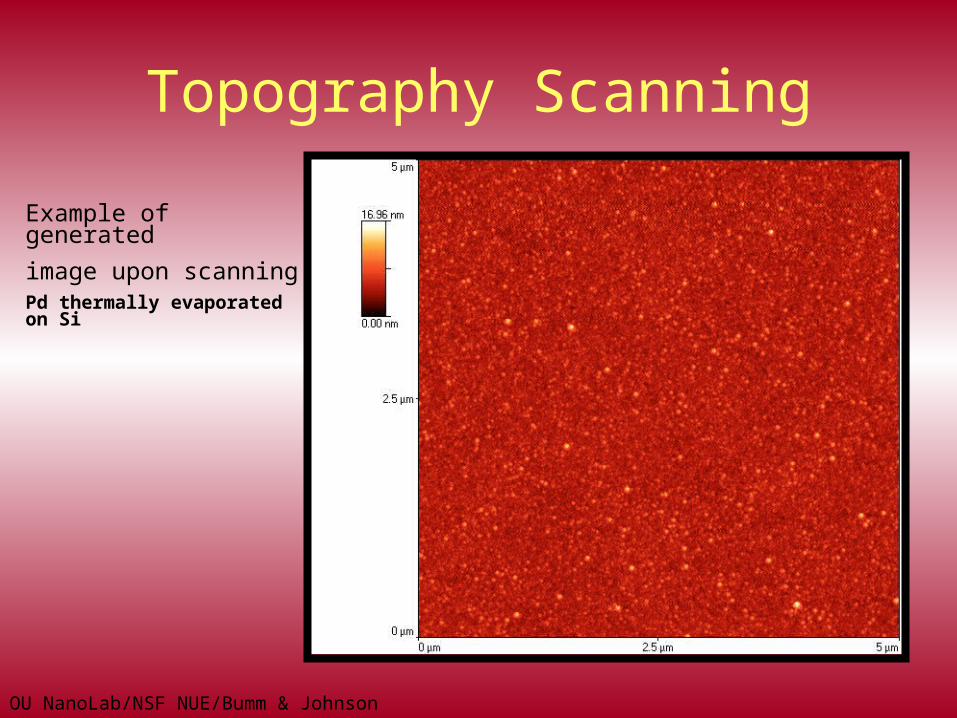
Topography Scanning
Example of generated
image upon scanningPd thermally evaporated on Si
OU NanoLab/NSF NUE/Bumm & Johnson
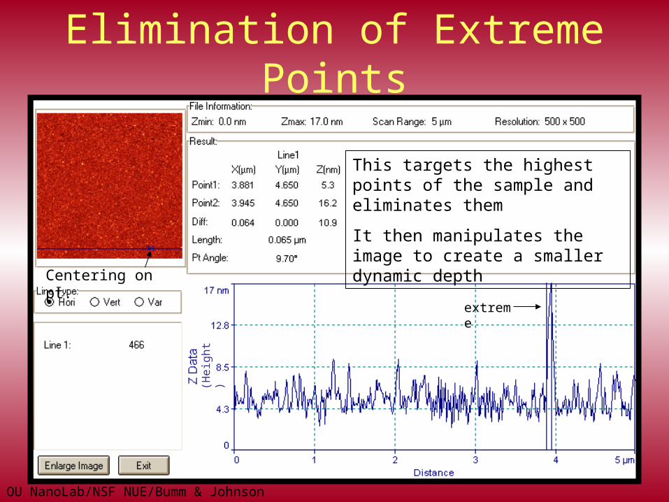
This targets the highest points of the sample and eliminates them
It then manipulates the image to create a smaller dynamic depth
extreme
(He
igh
t)
Centering on pt.
Elimination of Extreme Points
OU NanoLab/NSF NUE/Bumm & Johnson
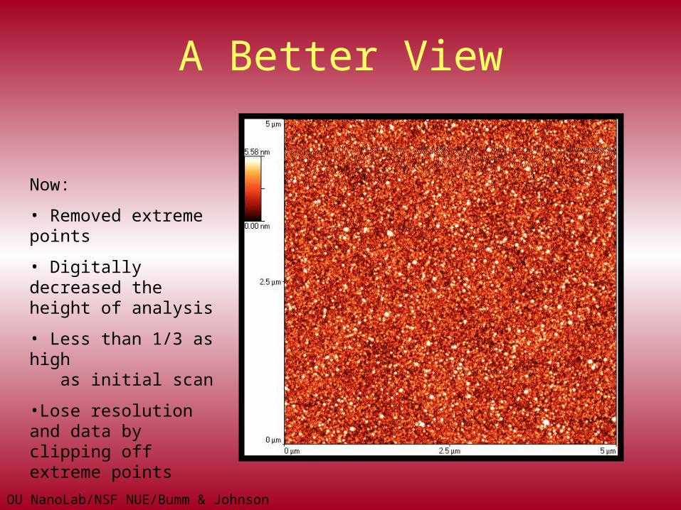
A Better View
Now:
• Removed extreme points
• Digitally decreased the height of analysis
• Less than 1/3 as high as initial scan
•Lose resolution and data by clipping off extreme points
OU NanoLab/NSF NUE/Bumm & Johnson
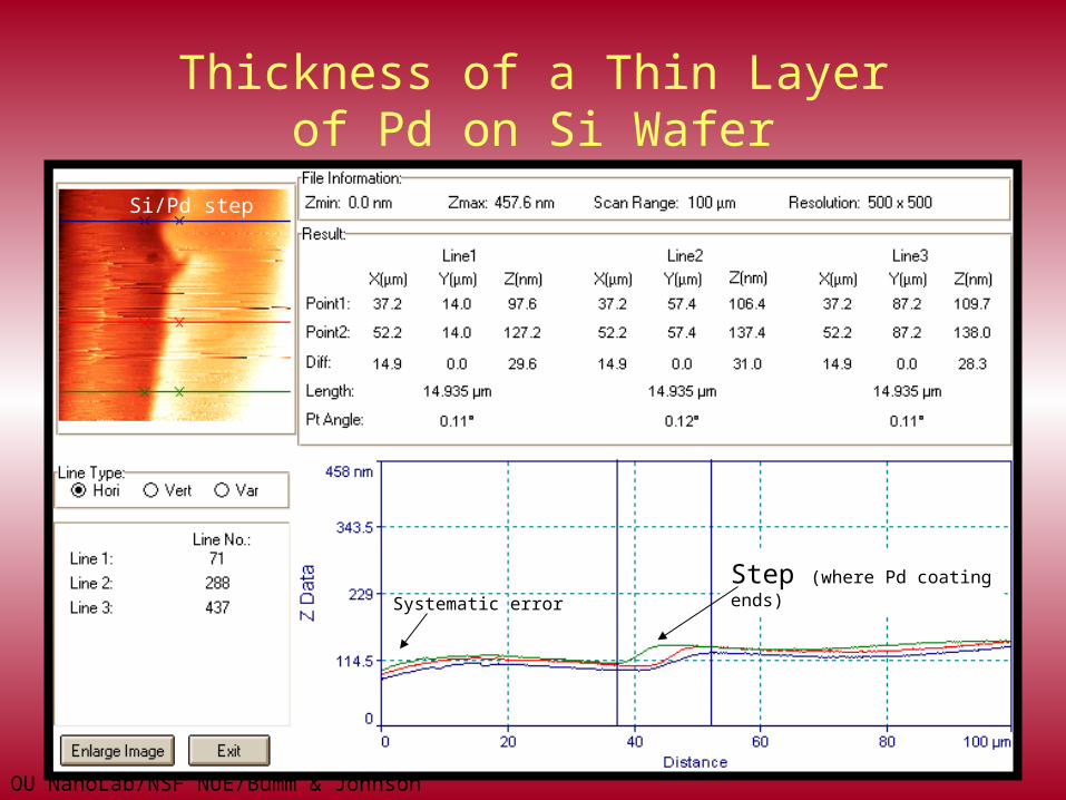
Si/Pd step
Thickness of a Thin Layerof Pd on Si Wafer
Step (where Pd coating ends)
Systematic error
OU NanoLab/NSF NUE/Bumm & Johnson
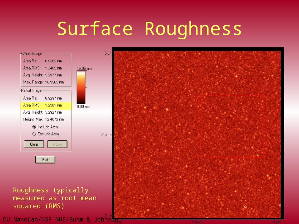
Surface Roughness
Roughness typically measured as root mean squared (RMS)
OU NanoLab/NSF NUE/Bumm & Johnson
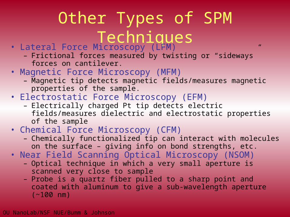
Other Types of SPM Techniques• Lateral Force Microscopy (LFM)
– Frictional forces measured by twisting or “sideways” forces on cantilever.
• Magnetic Force Microscopy (MFM)– Magnetic tip detects magnetic fields/measures magnetic properties
of the sample.• Electrostatic Force Microscopy (EFM)
– Electrically charged Pt tip detects electric fields/measures dielectric and electrostatic properties of the sample
• Chemical Force Microscopy (CFM)– Chemically functionalized tip can interact with molecules on the
surface – giving info on bond strengths, etc.• Near Field Scanning Optical Microscopy (NSOM)
– Optical technique in which a very small aperture is scanned very close to sample
– Probe is a quartz fiber pulled to a sharp point and coated with aluminum to give a sub-wavelength aperture (~100 nm)
OU NanoLab/NSF NUE/Bumm & Johnson
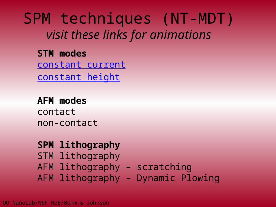
STM modesconstant currentconstant height
AFM modescontactnon-contact
SPM lithographySTM lithographyAFM lithography – scratchingAFM lithography – Dynamic Plowing
SPM techniques (NT-MDT)visit these links for animations
OU NanoLab/NSF NUE/Bumm & Johnson
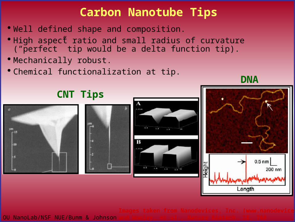
Carbon Nanotube Tips Well defined shape and composition. High aspect ratio and small radius of curvature (“perfect” tip would be a delta
function tip). Mechanically robust. Chemical functionalization at tip.
DNA
CNT Tips
Images taken from Nanodevices, Inc. (www.nanodevices.com)and Wooley, et al., Nature Biotech. 18, 760
OU NanoLab/NSF NUE/Bumm & Johnson
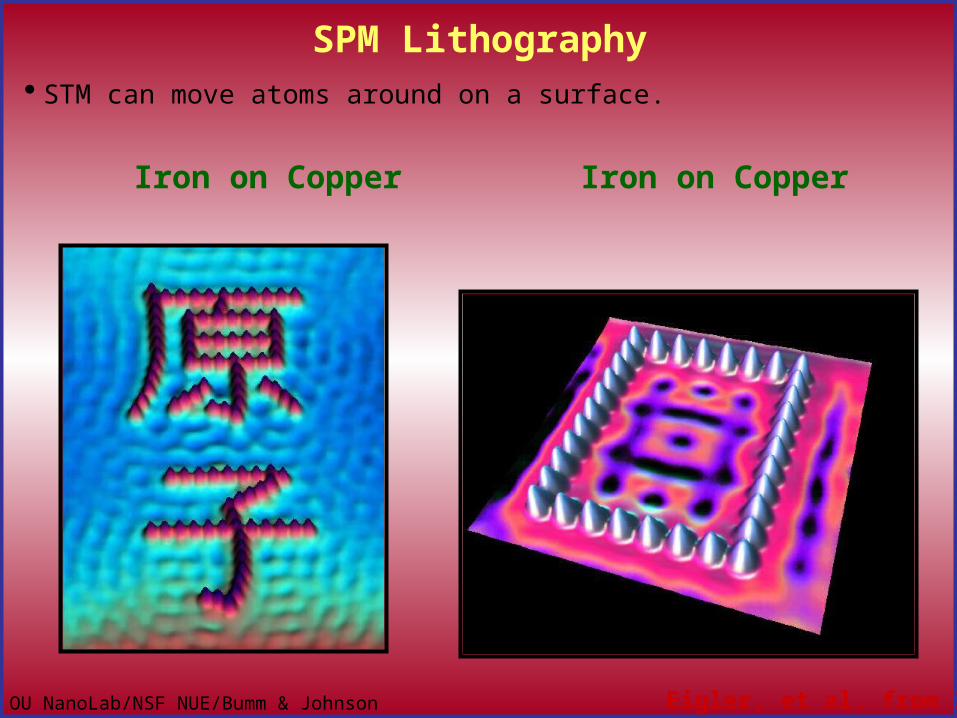
STM can move atoms around on a surface.
SPM Lithography
Iron on Copper Iron on Copper
Eigler, et al. from IBM
OU NanoLab/NSF NUE/Bumm & Johnson
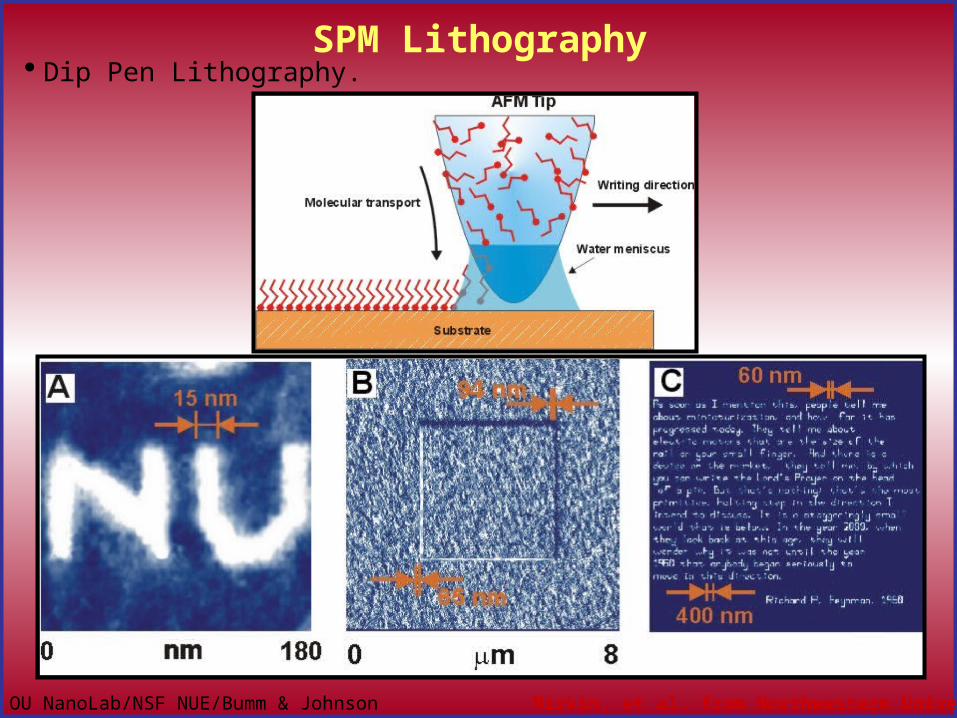
Dip Pen Lithography.SPM Lithography
Mirkin, et al. from Northwestern University
OU NanoLab/NSF NUE/Bumm & Johnson
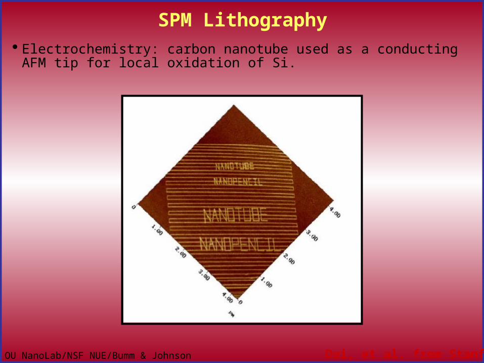
Electrochemistry: carbon nanotube used as a conducting AFM tip for local oxidation of Si.
SPM Lithography
Dai, et al. from Stanford
OU NanoLab/NSF NUE/Bumm & Johnson
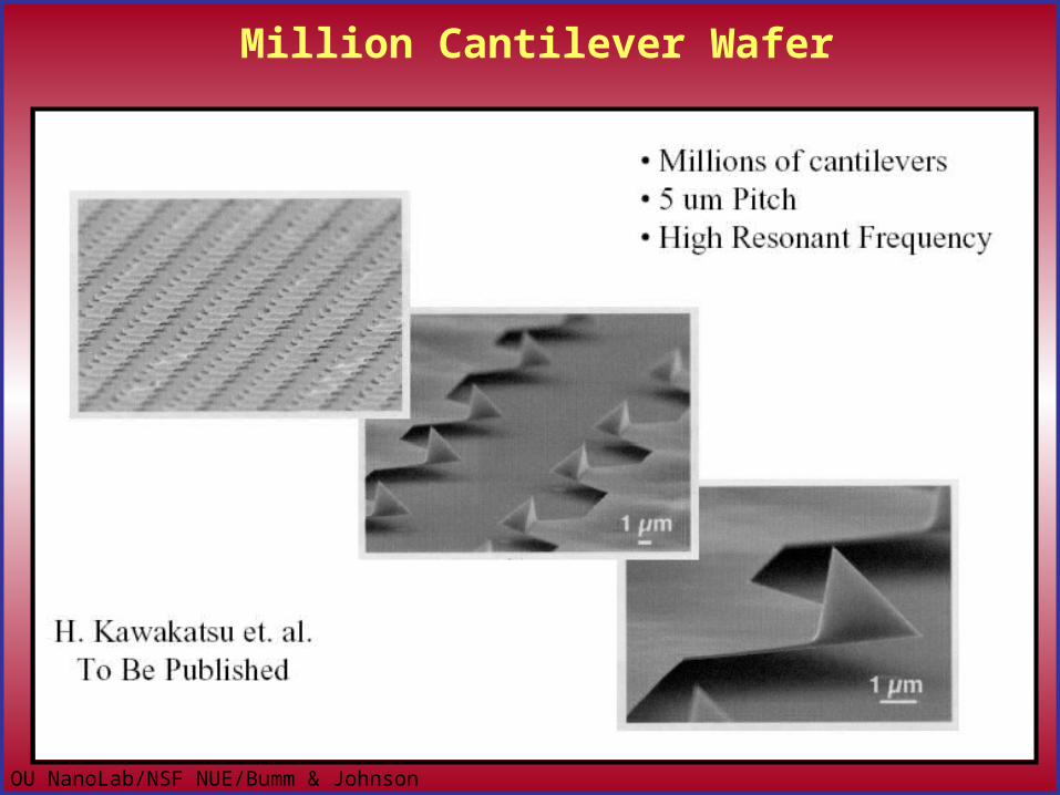
Million Cantilever Wafer
OU NanoLab/NSF NUE/Bumm & Johnson
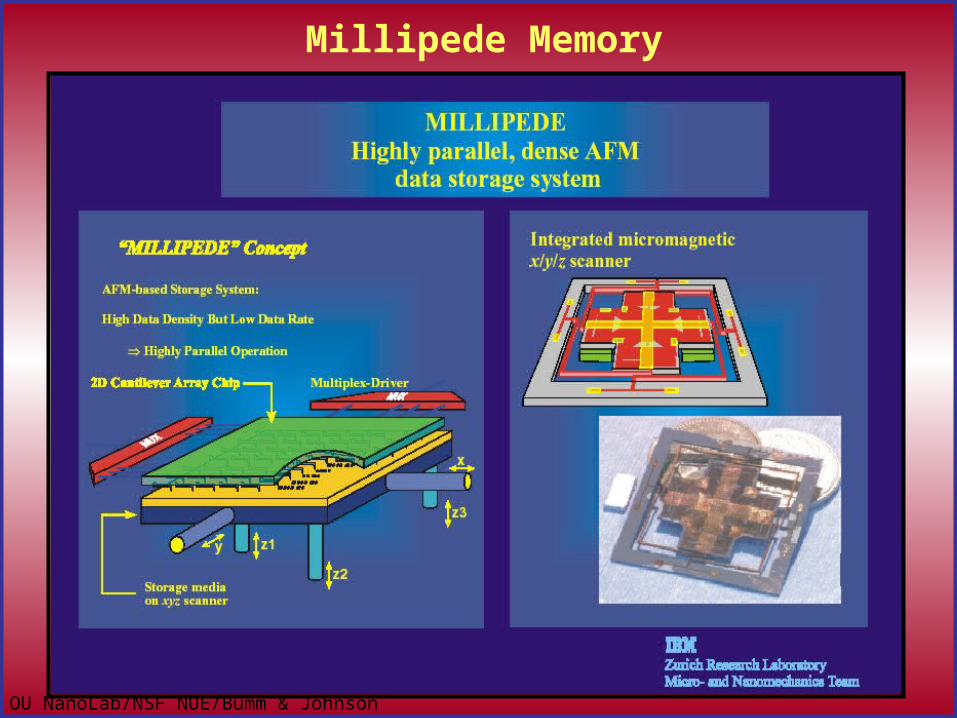
Millipede Memory
OU NanoLab/NSF NUE/Bumm & Johnson
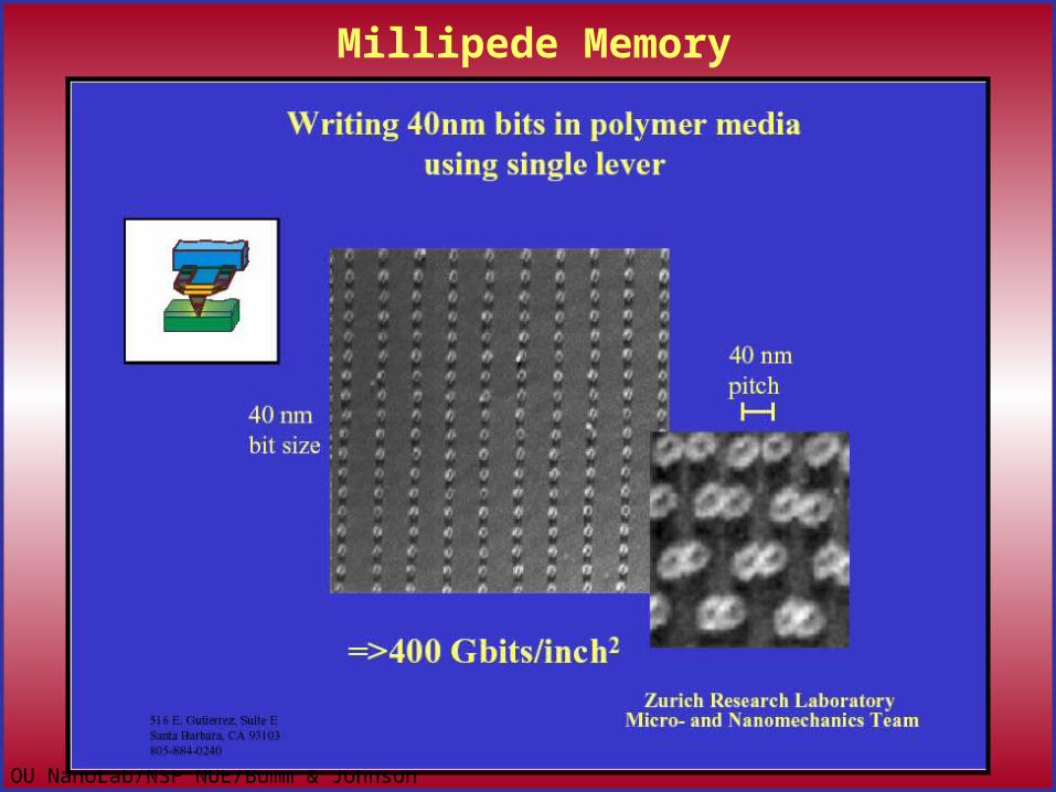
Millipede Memory
OU NanoLab/NSF NUE/Bumm & Johnson
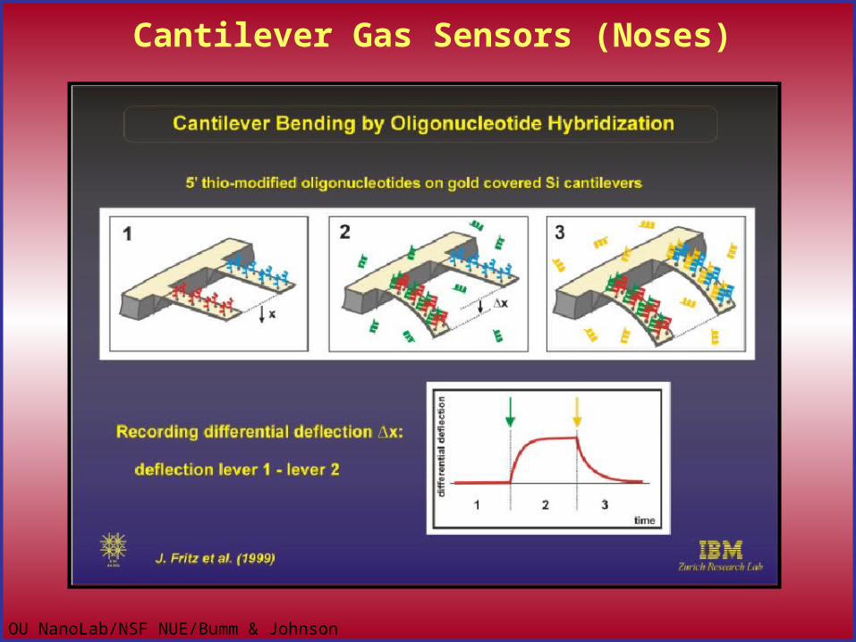
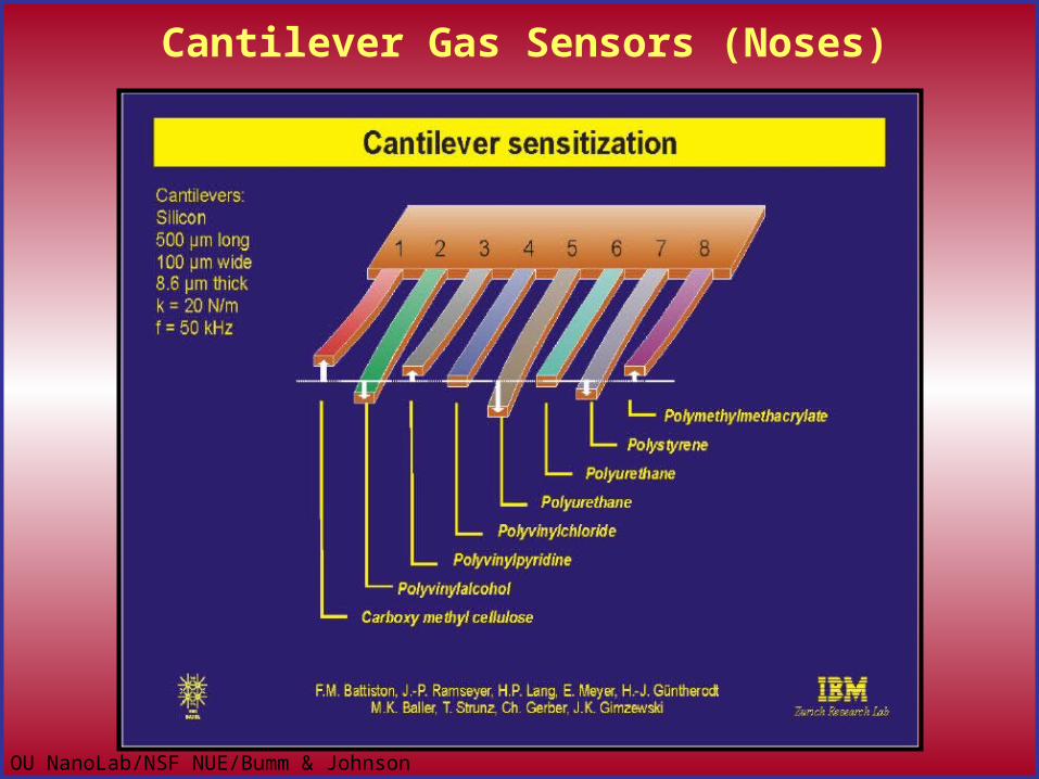
Cantilever Gas Sensors (Noses)
OU NanoLab/NSF NUE/Bumm & Johnson
Cantilever Gas Sensors (Noses)


