1. General description The P82B96 is a bipolar IC that creates a non-latching, bidirectional, logic interface between the normal I 2 C-bus and a range of other bus configurations. It can interface I 2 C-bus logic signals to similar buses having different voltage and current levels. For example, it can interface to the 350 μA SMBus, to 3.3 V logic devices, and to 15 V levels and/or low-impedance lines to improve noise immunity on longer bus lengths. It achieves this interface without any restrictions on the normal I 2 C-bus protocols or clock speed. The IC adds minimal loading to the I 2 C-bus node, and loadings of the new bus or remote I 2 C-bus nodes are not transmitted or transformed to the local node. Restrictions on the number of I 2 C-bus devices in a system, or the physical separation between them, are virtually eliminated. Transmitting SDA and SCL signals via balanced transmission lines (twisted pairs) or with galvanic isolation (opto-coupling) is simple because separate directional Tx and Rx signals are provided. The Tx and Rx signals may be directly connected, without causing latching, to provide an alternative bidirectional signal line with I 2 C-bus properties. 2. Features ■ Bidirectional data transfer of I 2 C-bus signals ■ Isolates capacitance allowing 400 pF on Sx/Sy side and 4000 pF on Tx/Ty side ■ Tx/Ty outputs have 60 mA sink capability for driving low-impedance or high capacitive buses ■ 400 kHz operation over at least 20 meters of wire (see AN10148) ■ Supply voltage range of 2 V to 15 V with I 2 C-bus logic levels on Sx/Sy side independent of supply voltage ■ Splits I 2 C-bus signal into pairs of forward/reverse Tx/Rx, Ty/Ry signals for interface with opto-electrical isolators and similar devices that need unidirectional input and output signal paths. ■ Low power supply current ■ ESD protection exceeds 3500 V HBM per JESD22-A114, 250 V DIP package, 400 V SO package MM per JESD22-A115, and 1000 V CDM per JESD22-C101 ■ Latch-up free (bipolar process with no latching structures) ■ Packages offered: DIP8, SO8 and TSSOP8 P82B96 Dual bidirectional bus buffer Rev. 08 — 10 November 2009 Product data sheet
Transcript
1. General description
The P82B96 is a bipolar IC that creates a non-latching, bidirectional, logic interfacebetween the normal I2C-bus and a range of other bus configurations. It can interfaceI2C-bus logic signals to similar buses having different voltage and current levels.
For example, it can interface to the 350 µA SMBus, to 3.3 V logic devices, and to 15 Vlevels and/or low-impedance lines to improve noise immunity on longer bus lengths.
It achieves this interface without any restrictions on the normal I2C-bus protocols or clockspeed. The IC adds minimal loading to the I2C-bus node, and loadings of the new bus orremote I2C-bus nodes are not transmitted or transformed to the local node. Restrictionson the number of I2C-bus devices in a system, or the physical separation between them,are virtually eliminated. Transmitting SDA and SCL signals via balanced transmissionlines (twisted pairs) or with galvanic isolation (opto-coupling) is simple because separatedirectional Tx and Rx signals are provided. The Tx and Rx signals may be directlyconnected, without causing latching, to provide an alternative bidirectional signal line withI2C-bus properties.
2. Features
n Bidirectional data transfer of I2C-bus signals
n Isolates capacitance allowing 400 pF on Sx/Sy side and 4000 pF on Tx/Ty side
n Tx/Ty outputs have 60 mA sink capability for driving low-impedance or high capacitivebuses
n 400 kHz operation over at least 20 meters of wire (see AN10148)
n Supply voltage range of 2 V to 15 V with I2C-bus logic levels on Sx/Sy sideindependent of supply voltage
n Splits I2C-bus signal into pairs of forward/reverse Tx/Rx, Ty/Ry signals for interfacewith opto-electrical isolators and similar devices that need unidirectional input andoutput signal paths.
n Low power supply current
n ESD protection exceeds 3500 V HBM per JESD22-A114, 250 V DIP package, 400 VSO package MM per JESD22-A115, and 1000 V CDM per JESD22-C101
n Latch-up free (bipolar process with no latching structures)
n Packages offered: DIP8, SO8 and TSSOP8
P82B96Dual bidirectional bus bufferRev. 08 — 10 November 2009 Product data sheet
NXP Semiconductors P82B96Dual bidirectional bus buffer
3. Applications
n Interface between I2C-buses operating at different logic levels (for example, 5 V and3 V or 15 V)
n Interface between I2C-bus and SMBus (350 µA) standard
n Simple conversion of I2C-bus SDA or SCL signals to multi-drop differential bushardware, for example, via compatible PCA82C250
n Interfaces with opto-couplers to provide opto-isolation between I2C-bus nodes up to400 kHz
4. Ordering information
4.1 Ordering options
Table 1. Ordering information
Type number Package
Name Description Version
P82B96DP TSSOP8 plastic thin shrink small outline package; 8 leads;body width 3 mm
Product data sheet Rev. 08 — 10 November 2009 3 of 32
NXP Semiconductors P82B96Dual bidirectional bus buffer
7. Functional description
Refer to Figure 1 “Block diagram of P82B96”.
The P82B96 has two identical buffers allowing buffering of both of the I2C-bus (SDA andSCL) signals. Each buffer is made up of two logic signal paths, a forward path from theI2C-bus interface pin which drives the buffered bus, and a reverse signal path from thebuffered bus input to drive the I2C-bus interface. Thus these paths are:
• sense the voltage state of the I2C-bus pin Sx (or Sy) and transmit this state to the pinTx (Ty respectively), and
• sense the state of the pin Rx (Ry) and pull the I2C-bus pin LOW whenever Rx (Ry) isLOW.
The rest of this discussion will address only the ‘x’ side of the buffer; the ‘y’ side isidentical.
The I2C-bus pin (Sx) is designed to interface with a normal I2C-bus.
The logic threshold voltage levels on the I2C-bus are independent of the IC supply VCC.The maximum I2C-bus supply voltage is 15 V and the guaranteed static sink current is3 mA.
The logic level of Rx is determined from the power supply voltage VCC of the chip. LogicLOW is below 42 % of VCC, and logic HIGH is above 58 % of VCC (with a typical switchingthreshold of half VCC).
Tx is an open-collector output without ESD protection diodes to VCC. It may be connectedvia a pull-up resistor to a supply voltage in excess of VCC, as long as the 15 V rating is notexceeded. It has a larger current sinking capability than a normal I2C-bus device, beingable to sink a static current of greater than 30 mA, and typical 100 mA dynamic pull-downcapability as well.
A logic LOW is only transmitted to Tx when the voltage at the I2C-bus pin (Sx) is below0.6 V. A logic LOW at Rx will cause the I2C-bus (Sx) to be pulled to a logic LOW level inaccordance with I2C-bus requirements (maximum 1.5 V in 5 V applications) but not lowenough to be looped back to the Tx output and cause the buffer to latch LOW.
The minimum LOW level this chip can achieve on the I2C-bus by a LOW at Rx is typically0.8 V.
If the supply voltage VCC fails, then neither the I2C-bus nor the Tx output will be held LOW.Their open-collector configuration allows them to be pulled up to the rated maximum of15 V even without VCC present. The input configuration on Sx and Rx also present noloading of external signals even when VCC is not present.
The effective input capacitance of any signal pin, measured by its effect on bus rise times,is less than 7 pF for all bus voltages and supply voltages including VCC = 0 V.
Remark: Two or more Sx or Sy I/Os must not be interconnected. The P82B96 designdoes not support this configuration. Bidirectional I2C-bus signals do not allow anydirection control pin so, instead, slightly different logic low voltage levels are used at Sx/Syto avoid latching of this buffer. A ‘regular I2C-bus LOW’ applied at the Rx/Ry of a P82B96will be propagated to Sx/Sy as a ‘buffered LOW’ with a slightly higher voltage level. If this
Product data sheet Rev. 08 — 10 November 2009 4 of 32
NXP Semiconductors P82B96Dual bidirectional bus buffer
special ‘buffered LOW’ is applied to the Sx/Sy of another P82B96 that second P82B96 willnot recognize it as a ‘regular I2C-bus LOW’ and will not propagate it to its Tx/Ty output.The Sx/Sy side of P82B96 may not be connected to similar buffers that rely on speciallogic thresholds for their operation, for example PCA9511, PCA9515, or PCA9518. TheSx/Sy side is only intended for, and compatible with, the normal I2C-bus logic voltagelevels of I2C-bus master and slave chips, or even Tx/Rx signals of a second P82B96 ifrequired. The Tx/Rx and Ty/Ry I/O pins use the standard I2C-bus logic voltage levels of allI2C-bus parts. There are no restrictions on the interconnection of the Tx/Rx and Ty/Ry I/Opins to other P82B96s, for example in a star or multipoint configuration with the Tx/Rx andTy/Ry I/O pins on the common bus and the Sx/Sy side connected to the line card slavedevices. For more details see Application Note AN255.
8. Limiting values
[1] See also Section 10.2 “Negative undershoot below absolute minimum value”.
Table 4. Limiting valuesIn accordance with the Absolute Maximum Rating System (IEC 60134).Voltages with respect to pin GND.
Symbol Parameter Conditions Min Max Unit
VCC supply voltage VCC to GND −0.3 +18 V
VSx voltage on pin Sx I2C-bus SDA or SCL −0.3 +18 V
VTx voltage on pin Tx buffered output [1] −0.3 +18 V
VRx voltage on pin Rx receive input [1] −0.3 +18 V
In current on any pin - 250 mA
Ptot total power dissipation - 300 mW
Tj junction temperature operating rangeP82B96TD/S900
Product data sheet Rev. 08 — 10 November 2009 7 of 32
NXP Semiconductors P82B96Dual bidirectional bus buffer
[1] Limit data for +125 °C applies to P82B96TD/S900 version. It is guaranteed by design/characterization, but not by 100 % test.
[2] The minimum value requirement for pull-up current, 200 µA, guarantees that the minimum value for VSx output LOW will always exceedthe minimum VSx input HIGH level to eliminate any possibility of latching. The specified difference is guaranteed by design within any IC.While the tolerances on absolute levels allow a small probability the LOW from one Sx output is recognized by an Sx input of anotherP82B96, this has no consequences for normal applications. In any design the Sx pins of different ICs should never be linked becausethe resulting system would be very susceptible to induced noise and would not support all I2C-bus operating modes.
[3] The output logic LOW depends on the sink current. For scaling, see Application Note AN255.
[4] The input logic threshold is independent of the supply voltage.
[5] The fall time of VTx from 5 V to 2.5 V in the test is approximately 15 ns.
The fall time of VSx from 5 V to 2.5 V in the test is approximately 50 ns.
The rise time of VTx from 0 V to 2.5 V in the test is approximately 20 ns.
The rise time of VSx from 0.9 V to 2.5 V in the test is approximately 70 ns.
Tfall delayVRx toVSx, VRyto VSy
buffer time delay onfalling input betweenVRx = input switchingthreshold, and VSxoutput falling 50 %
RSx pull-up = 1500 Ω;no capacitive load;VCC = 5 V
- 250 - - - ns
Trise delayVRx toVSx, VRyto VSy
buffer time delay onrising input betweenVRx = input switchingthreshold, and VSxoutput reaching 50 %VCC
RSx pull-up = 1500 Ω;no capacitive load;VCC = 5 V
- 270 - - - ns
Input capacitance
Ci input capacitance effective inputcapacitance of anysignal pin measuredby incremental busrise times
- - 7 - 7 pF
Table 5. Characteristics …continuedTamb = +25 °C; voltages are specified with respect to GND with VCC = 5 V, unless otherwise specified.
Symbol Parameter Conditions Tamb = +25 °C Tamb = −40 °C to+125 °C[1]
Product data sheet Rev. 08 — 10 November 2009 10 of 32
NXP Semiconductors P82B96Dual bidirectional bus buffer
Figure 13 shows how a master I2C-bus can be protected against short circuits or failuresin applications that involve plug and socket connections and long cables that may becomedamaged. A simple circuit is added to monitor the SDA bus, and if its LOW time exceedsthe design value, then the master bus is disconnected. P82B96 will free all its I/Os if itssupply is removed, so one option is to connect its VCC to the output of a logic gate from,say, the 74LVC family. The SDA and SCL lines could be timed and VCC disabled via thegate if one or other lines exceeds a design value of ‘LOW’ period as in Figure 28 ofAN255. If the supply voltage of logic gates restricts the choice of VCC supply then thelow-cost discrete circuit in Figure 13 can be used. If the SDA line is held LOW, the 100 nFcapacitor will charge and the Ry input will be pulled towards VCC. When it exceeds 0.5VCCthe Ry input will set the Sy input HIGH, which in practice means simply releasing it.
In this example the SCL line is made unidirectional by tying the Rx pin to VCC. The state ofthe buffered SCL line cannot affect the master clock line which is allowed whenclock-stretching is not required. It is simple to add an additional transistor or diode tocontrol the Rx input in the same way as Ry when necessary. The +V cable drive can beany voltage up to 15 V and the bus may be run at a lower impedance by selecting pull-upresistors for a static sink current up to 30 mA. VCC1 and VCC2 may be chosen to suit theconnected devices. Because DDC uses relatively low speeds (< 100 kHz), the cablelength is not restricted to 20 m by the I2C-bus signalling, but it may be limited by the videosignalling.
Product data sheet Rev. 08 — 10 November 2009 11 of 32
NXP Semiconductors P82B96Dual bidirectional bus buffer
Figure 14 shows that P82B96 can achieve high clock rates over long cables. Whilecalculating with lumped wiring capacitance yields reasonable approximations to actualtiming, even 25 meters of cable is better treated using transmission line theory. Flat ribboncables connected as shown, with the bus signals on the outer edge, will have acharacteristic impedance in the range 100 Ω to 200 Ω. For simplicity they cannot beterminated in their characteristic impedance but a practical compromise is to use theminimum pull-up allowed for P82B96 and place half this termination at each end of thecable. When each pull-up is below 330 Ω, the rising edge waveforms have their firstvoltage ‘step’ level above the logic threshold at Rx and cable timing calculations can bebased on the fast rise/fall times of resistive loading plus simple one-way propagationdelays. When the pull-up is larger, but below 750 Ω, the threshold at Rx will be crossedafter one signal reflection. So at the sending end it is crossed after 2 times the one-waypropagation delay and at the receiving end after 3 times that propagation delay. For flatcables with partial plastic dielectric insulation (by using outer cores) the one-waypropagation delays will be about 5 ns per meter. The 10 % to 90 % rise and fall times onthe cable will be between 20 ns and 50 ns, so their delay contributions are small. Therewill be ringing on falling edges that can be damped, if required, by using Schottky diodesas shown.
When the Master SCL HIGH and LOW periods can be programmed separately, forexample using control registers I2SCLH and I2SCLL of 89LPC932, the timings can allowfor bus delays. The LOW period should be programmed to achieve the minimum 1300 nsplus the net delay in the slave's response data signal caused by bus and buffer delays.The longest data delay is the sum of the delay of the falling edge of SCL from master toslave and the delay of the rising edge of SDA from slave data to master. Because thebuffer will ‘stretch’ the programmed SCL LOW period, the actual SCL frequency will belower than calculated from the programmed clock periods. In the example for 25 metersthe clock is stretched 400 ns, the falling edge of SCL is delayed 490 ns and the SDA risingedge is delayed 570 ns. The required additional LOW period is(490 ns + 570 ns) = 1060 ns and the I2C-bus specifications already include an allowancefor a worst case bus rise time 0 % to 70 % of 425 ns. (The bus rise time can be 300 ns30 % to 70 %, which means it can be 425 ns 0 % to 70 %. The 25 meter cable delay timesas quoted already include all rise and fall times.) Therefore, the microcontroller only needsto be programmed with an additional (1060 ns − 400 ns − 425 ns) = 235 ns, making atotal programmed LOW period 1535 ns. The programmed LOW will the be stretched by400 ns to yield an actual bus LOW time of 1935 ns, which, allowing the minimum HIGHperiod of 600 ns, yields a cycle period of 2535 ns or 394 kHz.
Note that in both the 100 meter and 250 meter examples, the capacitive loading on theI2C-buses at each end is within the maximum allowed Standard mode loading of 400 pF,but exceeds the Fast mode limit. This is an example of a ‘hybrid’ mode because it relies onthe response delays of Fast mode parts but uses (allowable) Standard mode bus loadingswith rise times that contribute significantly to the system delays. The cables cause largepropagation delays, so these systems need to operate well below the 400 kHz limit, butillustrate how they can still exceed the 100 kHz limit provided all parts are capable ofFast mode operation. The fastest example illustrates how the 400 kHz limit can beexceeded, provided masters and slaves have the required timings, namely smaller thanthe maximum allowed for Fast mode. Many NXP slaves have delays shorter than 600 nsand all Fm+ devices must be < 450 ns.
Product data sheet Rev. 08 — 10 November 2009 13 of 32
xxxxxxxxxxxxxxxxxxxxx xxxxxxxxxxxxxxxxxxxxxxxxxx xxxxxxx x x x xxxxxxxxxxxxxxxxxxxxxxxxxxxxxx xxxxxxxxxxxxxxxxxxx xx xxxxxxx xxxxxxxxxxxxxxxxxxxxxxxxxxx xxxxxxxxxxxxxxxxxxx xxxxxx xxxxxxxxxxxxxxxxxxxxxxxxxxxxxxxxxxx xxxxxxxxxxxx x xxxxxxxxxxxxxxxxxxxxxx xxxxxxxxxxxxxxxxxxxxxxxxxxxxxx xxxxx xxxxxxxxxxxxxxxxxxxxxxxxxxxxxxxxxxxxxxxxxxxxxxxxxx xxxxxxxxxxxxxxxxxxxxxxxxxxxxxxxxx xxxxxxxxxxxxxxxxxxxx xxx
P82B
96_8
Product data shee
NX
P S
emiconductors
P82B
96D
ual bidirectional bus buffer
Table 6. Examples of bus capabilityRefer to Figure 14.
Product data sheet Rev. 08 — 10 November 2009 15 of 32
NXP Semiconductors P82B96Dual bidirectional bus buffer
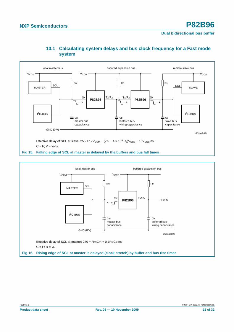
Figure 15, Figure 16, and Figure 17 show the P82B96 used to drive extended bus wiring,with relatively large capacitance, linking two Fast mode I2C-bus nodes. It includessimplified expressions for making the relevant timing calculations for 3.3 V or 5 Voperation. Because the buffers and the wiring introduce timing delays, it may benecessary to decrease the nominal SCL frequency below 400 kHz. In most cases theactual bus frequency will be lower than the nominal Master timing due to bit-wisestretching of the clock periods.
The delay factors involved in calculation of the allowed bus speed are:
A — The propagation delay of the master signal through the buffers and wiring to theslave. The important delay is that of the falling edge of SCL because this edge ‘requests’the data or acknowledge from a slave. See Figure 15.
B — The effective stretching of the nominal LOW period of SCL at the master caused bythe buffer and bus rise times. See Figure 16.
C — The propagation delay of the slave's response signal through the buffers and wiringback to the master. The important delay is that of a rising edge in the SDA signal. Risingedges are always slower and are therefore delayed by a longer time than falling edges.(The rising edges are limited by the passive pull-up while falling edges are actively driven).See Figure 17.
The timing requirement in any I2C-bus system is that a slave's data response (which isprovided in response to a falling edge of SCL) must be received at the master before theend of the corresponding LOW period of SCL as appears on the bus wiring at the master.Since all slaves will, as a minimum, satisfy the worst case timing requirements of a400 kHz part, they must provide their response within the minimum allowed clock LOWperiod of 1300 ns. Therefore in systems that introduce additional delays it is onlynecessary to extend that minimum clock LOW period by any ‘effective’ delay of the slave'sresponse. The effective delay of the slaves response equals the total delays in SCL falling
Effective delay of SDA at master = 270 + 0.2RsCs + 0.7 (RbCb + RmCm) ns.
C = F; R = Ω.
Fig 17. Rising edge of SDA at slave is delayed by the buffers and bus rise times
Product data sheet Rev. 08 — 10 November 2009 16 of 32
NXP Semiconductors P82B96Dual bidirectional bus buffer
edge from the master reaching the slave (Figure 15) minus the effective delay (stretch) ofthe SCL rising edge (Figure 16) plus total delays in the slave's response data, carried onSDA, reaching the master (Figure 17).
The master microcontroller should be programmed to produce a nominal SCL LOWperiod = (1300 + A − B + C) ns, and should be programmed to produce the nominalminimum SCL HIGH period of 600 ns. Then a check should be made to ensure the cycletime is not shorter than the minimum 2500 ns. If found necessary, just increase eitherclock period.
Due to clock stretching, the SCL cycle time will always be longer than(600 + 1300 + A + C) ns.
Example:
The master bus has an RmCm product of 100 ns and VCCM = 5 V.
The buffered bus has a capacitance of 1 nF and a pull-up resistor of 160 Ω to 5 V givingan RbCb product of 160 ns. The slave bus also has an RsCs product of 100 ns.
The microcontroller LOW period should be programmed to≥ (1300 + 372.5 − 482 + 472) ns, that is ≥ 1662.5 ns.
Its HIGH period may be programmed to the minimum 600 ns.
The nominal microcontroller clock period will be ≥ (1662.5 + 600) ns = 2262.5 ns,equivalent to a frequency of 442 kHz.
The actual bus clock period, including the 482 ns clock stretch effect, will be below(nominal + stretch) = (2262.5 + 482) ns or ≥ 2745 ns, equivalent to an allowablefrequency of 364 kHz.
Fig 18. I2C-bus multipoint application
P82B96
SDARx
SCL
Tx
Ty
Ry
002aab994
12 V
Sx
Sy
12 V
12 V3.3 V to 5 V
3.3 V to 5 V
P82B96
Sx Sy
SCL/SDA
P82B96
Sx Sy
SCL/SDA
P82B96
Sx Sy
SCL/SDA
P82B96
Sx SCL
Sy SDA
no limit to the number of connected bus devices
twitsted-pair telephone wires,USB, or flat ribbon cables; up to 15 V logic levels, include VCC and GND
Product data sheet Rev. 08 — 10 November 2009 17 of 32
NXP Semiconductors P82B96Dual bidirectional bus buffer
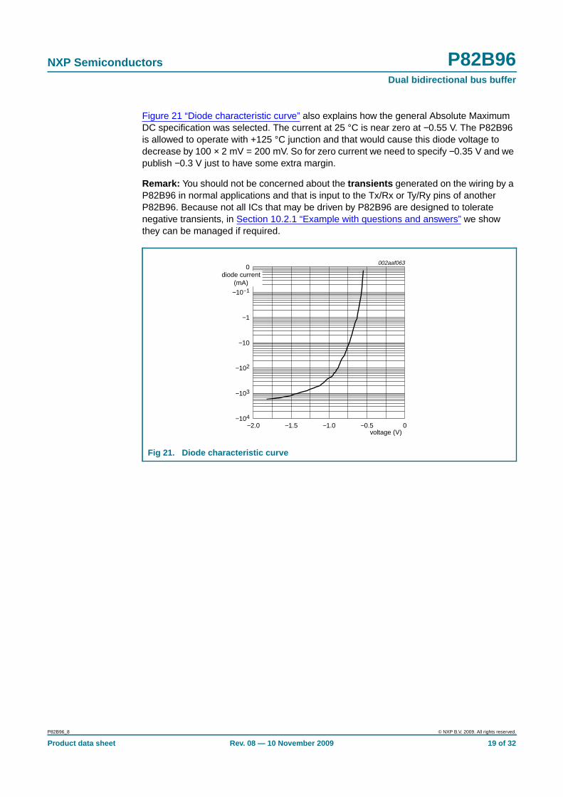
10.2 Negative undershoot below absolute minimum valueThe reason why the IC pin reverse voltage on pins Tx and Rx in Table 4 “Limiting values”is specified at such a low value, −0.3 V, is not that applying larger voltages is likely tocause damage but that it is expected that, in normal applications, there is no reason whylarger DC voltages will be applied. This ‘absolute maximum’ specification is intended to bea DC or continuous ratings and the nominal DC I2C-bus voltage LOW usually does noteven reach 0 V. Inside P82B96 at every pin there is a large protective diode connected tothe GND pin and that diode will start to conduct when the pin voltage is more than about−0.55 V with respect to GND at 25 °C ambient.
Figure 21 shows the measured characteristic for one of those diodes inside P82B96. Theplot was made using a curve tracer that applies 50 Hz mains voltage via a series resistor,so the pulse durations are long duration (several milliseconds) and are reaching peaks ofover 2 A when more than −1.5 V is applied. The IC becomes very hot during this testingbut it was not damaged. Whenever there is current flowing in any of these diodes it ispossible that there can be faulty operation of any IC. For that reason we put a specificationon the negative voltage that is allowed to be applied. It is selected so that, at the highestallowed junction temperature, there will be a big safety factor that guarantees the diodewill not conduct and then we do not need to make any 100 % production tests toguarantee the published specification.
For the P82B96, in specific applications, there will always be transient overshoot andringing on the wiring that can cause these diodes to conduct. Therefore we designed theIC to withstand those transients and as a part of the qualification procedure we madetests, using DC currents to more than twice the normal bus sink currents, to be sure thatthe IC was not affected by those currents. For example, the Tx/Ty and Rx/Ry pins weretested to at least −80 mA which, from Figure 21, would be more than −0.8 V. The correctfunctioning of the P82B96 is not affected even by those large currents. The AbsoluteMaximum (DC) ratings are not intended to apply to transients but to steady stateconditions. This explains why you will never see any problems in practice even if, duringtransients, more than −0.3 V is applied to the bus interface pins of P82B96.
Frequency = 624 kHz Ch1 frequency = 624 kHz
Fig 19. Propagation Sx to Tx (Sx pull-up to 5 V;Tx pull-up to V CC = 10 V)
Fig 20. Propagation Rx to Sx (Sx pull-up to 5 V;Rx pull-up to V CC = 10 V)
Product data sheet Rev. 08 — 10 November 2009 18 of 32
NXP Semiconductors P82B96Dual bidirectional bus buffer
Figure 21 “Diode characteristic curve” also explains how the general Absolute MaximumDC specification was selected. The current at 25 °C is near zero at −0.55 V. The P82B96is allowed to operate with +125 °C junction and that would cause this diode voltage todecrease by 100 × 2 mV = 200 mV. So for zero current we need to specify −0.35 V and wepublish −0.3 V just to have some extra margin.
Remark: You should not be concerned about the transients generated on the wiring by aP82B96 in normal applications and that is input to the Tx/Rx or Ty/Ry pins of anotherP82B96. Because not all ICs that may be driven by P82B96 are designed to toleratenegative transients, in Section 10.2.1 “Example with questions and answers” we showthey can be managed if required.
Product data sheet Rev. 08 — 10 November 2009 19 of 32
NXP Semiconductors P82B96Dual bidirectional bus buffer
10.2.1 Example with questions and answers
Question: On a falling edge of Tx we measure undershoot at −800 mV at the linked Tx,Rx pins of the P82B96 that is generating the LOW, but the P82B96 data sheet specifiesminimum −0.3 V. Does this mean that we violate the data sheet absolute value?
Answer: For P82B96 the −0.3 V Absolute Maximum rating is not intended to apply totransients, it is a DC rating. As shown in Figure 22, there is no theoretical reason for anyundershoot at the IC that is driving the bus LOW and no significant undershoot shouldbe observed when using reasonable care with the ground connection of the ‘scope. It ismore likely that undershoot observed at a driving P82B96 is caused by local strayinductance and capacitance in the circuit and by the oscilloscope connections. Asshown, undershoot will be generated by PCB traces, wiring, or cables driven by aP82B96 because the allowed value of the I2C-bus pull-up resistor generally is largerthan that required to correctly terminate the wiring. In this example, with no ICconnected at the end of the wiring, the undershoot is about 2 V.
Product data sheet Rev. 08 — 10 November 2009 20 of 32
NXP Semiconductors P82B96Dual bidirectional bus buffer
Question: We have 2 meters of cable in a bus that joins the Tx/Rx sides of two P82B96devices. When one Tx drives LOW the other P82B96 Tx/Rx is driven to −0.8 V for over50 ns. What is the expected value and the theoretically allowed value of undershoot?
Answer: Because the cable joining the two P82B96s is a ‘transmission line’ that willhave a characteristic impedance around 100 Ω and it will be terminated by pull-upresistors that are larger than that characteristic impedance there will always be negativeundershoot generated. The duration of the undershoot is a function of the cable lengthand the input impedance of the connected IC. As shown in Figure 23, the transientundershoot will be limited, by the diodes inside P82B96, to around −0.8 V and that willnot cause problems for P82B96. Those transients will not be passed inside the IC to theSx/Sy side of the IC.
Question: If we input 800 mV undershoot at Tx, Rx pins, what kind of problem isexpected?
Answer: When that undershoot is generated by another P82B96 and is simply theresult of the system wiring, then there will be no problems.
Question: Will we have any functional problem or reliability problem?
Answer: No.
Fig 23. Wiring transients limited by the diodes in P82B96
Product data sheet Rev. 08 — 10 November 2009 21 of 32
NXP Semiconductors P82B96Dual bidirectional bus buffer
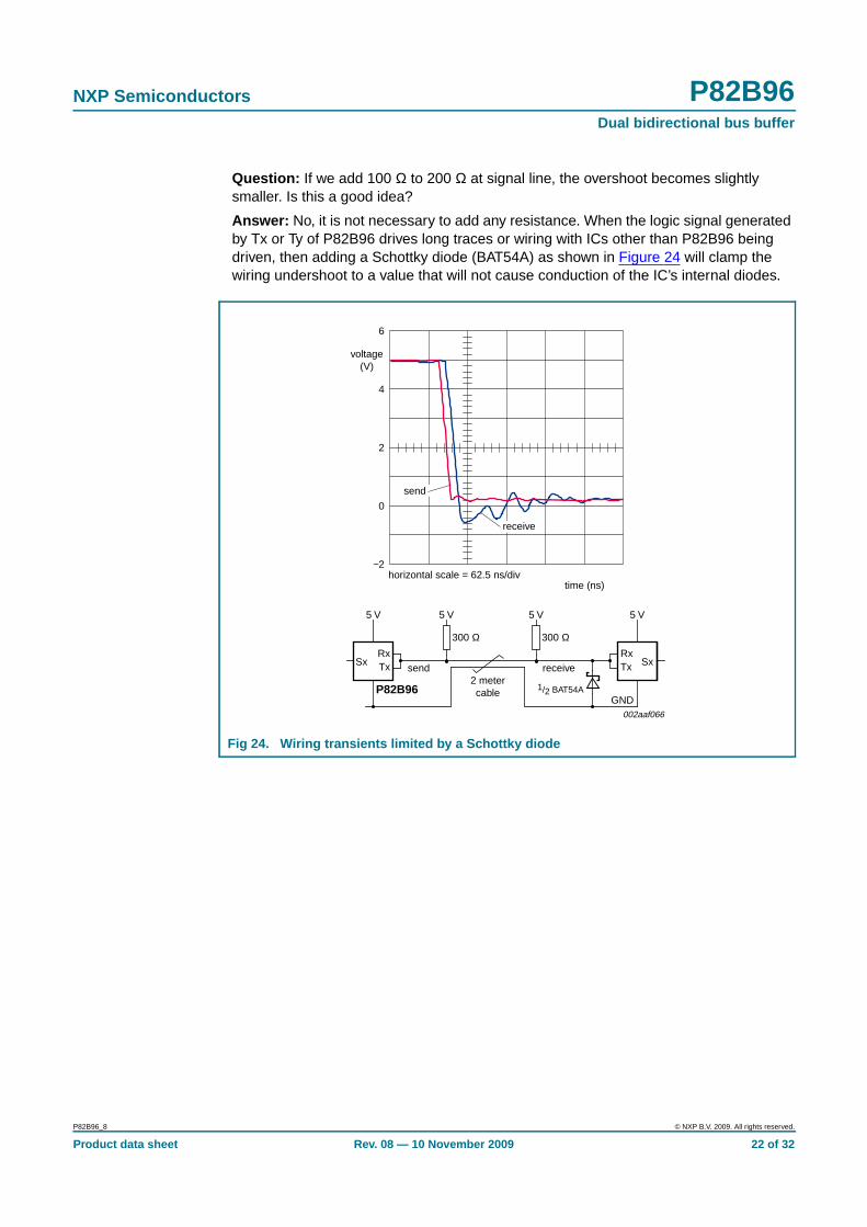
Question: If we add 100 Ω to 200 Ω at signal line, the overshoot becomes slightlysmaller. Is this a good idea?
Answer: No, it is not necessary to add any resistance. When the logic signal generatedby Tx or Ty of P82B96 drives long traces or wiring with ICs other than P82B96 beingdriven, then adding a Schottky diode (BAT54A) as shown in Figure 24 will clamp thewiring undershoot to a value that will not cause conduction of the IC’s internal diodes.
Fig 24. Wiring transients limited by a Schottky diode
Product data sheet Rev. 08 — 10 November 2009 25 of 32
NXP Semiconductors P82B96Dual bidirectional bus buffer
12. Soldering of SMD packages
This text provides a very brief insight into a complex technology. A more in-depth accountof soldering ICs can be found in Application Note AN10365 “Surface mount reflowsoldering description”.
12.1 Introduction to solderingSoldering is one of the most common methods through which packages are attached toPrinted Circuit Boards (PCBs), to form electrical circuits. The soldered joint provides boththe mechanical and the electrical connection. There is no single soldering method that isideal for all IC packages. Wave soldering is often preferred when through-hole andSurface Mount Devices (SMDs) are mixed on one printed wiring board; however, it is notsuitable for fine pitch SMDs. Reflow soldering is ideal for the small pitches and highdensities that come with increased miniaturization.
12.2 Wave and reflow solderingWave soldering is a joining technology in which the joints are made by solder coming froma standing wave of liquid solder. The wave soldering process is suitable for the following:
• Through-hole components
• Leaded or leadless SMDs, which are glued to the surface of the printed circuit board
Not all SMDs can be wave soldered. Packages with solder balls, and some leadlesspackages which have solder lands underneath the body, cannot be wave soldered. Also,leaded SMDs with leads having a pitch smaller than ~0.6 mm cannot be wave soldered,due to an increased probability of bridging.
The reflow soldering process involves applying solder paste to a board, followed bycomponent placement and exposure to a temperature profile. Leaded packages,packages with solder balls, and leadless packages are all reflow solderable.
Key characteristics in both wave and reflow soldering are:
• Board specifications, including the board finish, solder masks and vias
• Package footprints, including solder thieves and orientation
• The moisture sensitivity level of the packages
• Package placement
• Inspection and repair
• Lead-free soldering versus SnPb soldering
12.3 Wave solderingKey characteristics in wave soldering are:
• Process issues, such as application of adhesive and flux, clinching of leads, boardtransport, the solder wave parameters, and the time during which components areexposed to the wave
• Solder bath specifications, including temperature and impurities
Product data sheet Rev. 08 — 10 November 2009 26 of 32
NXP Semiconductors P82B96Dual bidirectional bus buffer
12.4 Reflow solderingKey characteristics in reflow soldering are:
• Lead-free versus SnPb soldering; note that a lead-free reflow process usually leads tohigher minimum peak temperatures (see Figure 28) than a SnPb process, thusreducing the process window
• Solder paste printing issues including smearing, release, and adjusting the processwindow for a mix of large and small components on one board
• Reflow temperature profile; this profile includes preheat, reflow (in which the board isheated to the peak temperature) and cooling down. It is imperative that the peaktemperature is high enough for the solder to make reliable solder joints (a solder pastecharacteristic). In addition, the peak temperature must be low enough that thepackages and/or boards are not damaged. The peak temperature of the packagedepends on package thickness and volume and is classified in accordance withTable 7 and 8
Moisture sensitivity precautions, as indicated on the packing, must be respected at alltimes.
Studies have shown that small packages reach higher temperatures during reflowsoldering, see Figure 28.
Table 7. SnPb eutectic process (from J-STD-020C)
Package thickness (mm) Package reflow temperature ( °C)
Volume (mm 3)
< 350 ≥ 350
< 2.5 235 220
≥ 2.5 220 220
Table 8. Lead-free process (from J-STD-020C)
Package thickness (mm) Package reflow temperature ( °C)
Product data sheet Rev. 08 — 10 November 2009 27 of 32
NXP Semiconductors P82B96Dual bidirectional bus buffer
For further information on temperature profiles, refer to Application Note AN10365“Surface mount reflow soldering description”.
13. Soldering of through-hole mount packages
13.1 Introduction to soldering through-hole mount packagesThis text gives a very brief insight into wave, dip and manual soldering.
Wave soldering is the preferred method for mounting of through-hole mount IC packageson a printed-circuit board.
13.2 Soldering by dipping or by solder waveDriven by legislation and environmental forces the worldwide use of lead-free solderpastes is increasing. Typical dwell time of the leads in the wave ranges from3 seconds to 4 seconds at 250 °C or 265 °C, depending on solder material applied, SnPbor Pb-free respectively.
The total contact time of successive solder waves must not exceed 5 seconds.
The device may be mounted up to the seating plane, but the temperature of the plasticbody must not exceed the specified maximum storage temperature (Tstg(max)). If theprinted-circuit board has been pre-heated, forced cooling may be necessary immediatelyafter soldering to keep the temperature within the permissible limit.
13.3 Manual solderingApply the soldering iron (24 V or less) to the lead(s) of the package, either below theseating plane or not more than 2 mm above it. If the temperature of the soldering iron bit isless than 300 °C it may remain in contact for up to 10 seconds. If the bit temperature isbetween 300 °C and 400 °C, contact may be up to 5 seconds.
MSL: Moisture Sensitivity Level
Fig 28. Temperature profiles for large and small components
001aac844
temperature
time
minimum peak temperature= minimum soldering temperature
Product data sheet Rev. 08 — 10 November 2009 30 of 32
NXP Semiconductors P82B96Dual bidirectional bus buffer
16. Legal information
16.1 Data sheet status
[1] Please consult the most recently issued document before initiating or completing a design.
[2] The term ‘short data sheet’ is explained in section “Definitions”.
[3] The product status of device(s) described in this document may have changed since this document was published and may differ in case of multiple devices. The latest product statusinformation is available on the Internet at URL http://www.nxp.com.
16.2 Definitions
Draft — The document is a draft version only. The content is still underinternal review and subject to formal approval, which may result inmodifications or additions. NXP Semiconductors does not give anyrepresentations or warranties as to the accuracy or completeness ofinformation included herein and shall have no liability for the consequences ofuse of such information.
Short data sheet — A short data sheet is an extract from a full data sheetwith the same product type number(s) and title. A short data sheet is intendedfor quick reference only and should not be relied upon to contain detailed andfull information. For detailed and full information see the relevant full datasheet, which is available on request via the local NXP Semiconductors salesoffice. In case of any inconsistency or conflict with the short data sheet, thefull data sheet shall prevail.
16.3 Disclaimers
General — Information in this document is believed to be accurate andreliable. However, NXP Semiconductors does not give any representations orwarranties, expressed or implied, as to the accuracy or completeness of suchinformation and shall have no liability for the consequences of use of suchinformation.
Right to make changes — NXP Semiconductors reserves the right to makechanges to information published in this document, including withoutlimitation specifications and product descriptions, at any time and withoutnotice. This document supersedes and replaces all information supplied priorto the publication hereof.
Suitability for use — NXP Semiconductors products are not designed,authorized or warranted to be suitable for use in medical, military, aircraft,space or life support equipment, nor in applications where failure ormalfunction of an NXP Semiconductors product can reasonably be expectedto result in personal injury, death or severe property or environmental
damage. NXP Semiconductors accepts no liability for inclusion and/or use ofNXP Semiconductors products in such equipment or applications andtherefore such inclusion and/or use is at the customer’s own risk.
Applications — Applications that are described herein for any of theseproducts are for illustrative purposes only. NXP Semiconductors makes norepresentation or warranty that such applications will be suitable for thespecified use without further testing or modification.
Limiting values — Stress above one or more limiting values (as defined inthe Absolute Maximum Ratings System of IEC 60134) may cause permanentdamage to the device. Limiting values are stress ratings only and operation ofthe device at these or any other conditions above those given in theCharacteristics sections of this document is not implied. Exposure to limitingvalues for extended periods may affect device reliability.
Terms and conditions of sale — NXP Semiconductors products are soldsubject to the general terms and conditions of commercial sale, as publishedat http://www.nxp.com/profile/terms, including those pertaining to warranty,intellectual property rights infringement and limitation of liability, unlessexplicitly otherwise agreed to in writing by NXP Semiconductors. In case ofany inconsistency or conflict between information in this document and suchterms and conditions, the latter will prevail.
No offer to sell or license — Nothing in this document may be interpretedor construed as an offer to sell products that is open for acceptance or thegrant, conveyance or implication of any license under any copyrights, patentsor other industrial or intellectual property rights.
Export control — This document as well as the item(s) described hereinmay be subject to export control regulations. Export might require a priorauthorization from national authorities.
16.4 TrademarksNotice: All referenced brands, product names, service names and trademarksare the property of their respective owners.
I2C-bus — logo is a trademark of NXP B.V.
17. Contact information
For more information, please visit: http://www .nxp.com
For sales office addresses, please send an email to: salesad [email protected]
Document status [1] [2] Product status [3] Definition
Objective [short] data sheet Development This document contains data from the objective specification for product development.
Preliminary [short] data sheet Qualification This document contains data from the preliminary specification.
Product [short] data sheet Production This document contains the product specification.