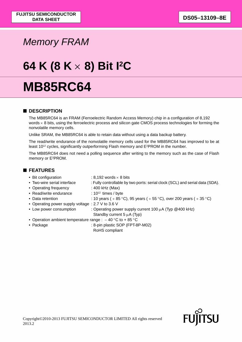
■ DESCRIPTIONThe MB85RC64 is an FRAM (Ferroelectric Random Access Memory) chip in a configuration of 8,192 words 8 bits, using the ferroelectric process and silicon gate CMOS process technologies for forming thenonvolatile memory cells.
Unlike SRAM, the MB85RC64 is able to retain data without using a data backup battery.
The read/write endurance of the nonvolatile memory cells used for the MB85RC64 has improved to be atleast 1012 cycles, significantly outperforming Flash memory and E2PROM in the number.
The MB85RC64 does not need a polling sequence after writing to the memory such as the case of Flashmemory or E2PROM.
■ FEATURES• Bit configuration : 8,192 words 8 bits• Two-wire serial interface : Fully controllable by two ports: serial clock (SCL) and serial data (SDA).• Operating frequency : 400 kHz (Max)• Read/write endurance : 1012 times / byte• Data retention : 10 years ( 85 C), 95 years ( 55 C), over 200 years ( 35 C)• Operating power supply voltage : 2.7 V to 3.6 V• Low power consumption : Operating power supply current 100 A (Typ @400 kHz)
Standby current 5 A (Typ)• Operation ambient temperature range : 40 C to + 85 C• Package : 8-pin plastic SOP (FPT-8P-M02)
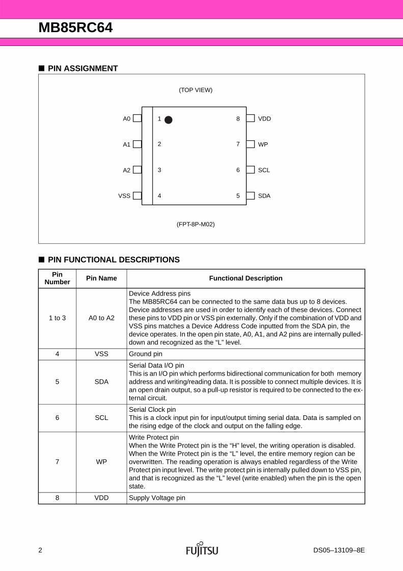
Device Address pinsThe MB85RC64 can be connected to the same data bus up to 8 devices. Device addresses are used in order to identify each of these devices. Connect these pins to VDD pin or VSS pin externally. Only if the combination of VDD and VSS pins matches a Device Address Code inputted from the SDA pin, the device operates. In the open pin state, A0, A1, and A2 pins are internally pulled-down and recognized as the “L” level.
4 VSS Ground pin
5 SDA
Serial Data I/O pinThis is an I/O pin which performs bidirectional communication for both memory address and writing/reading data. It is possible to connect multiple devices. It is an open drain output, so a pull-up resistor is required to be connected to the ex-ternal circuit.
6 SCLSerial Clock pinThis is a clock input pin for input/output timing serial data. Data is sampled on the rising edge of the clock and output on the falling edge.
7 WP
Write Protect pinWhen the Write Protect pin is the “H” level, the writing operation is disabled. When the Write Protect pin is the “L” level, the entire memory region can be overwritten. The reading operation is always enabled regardless of the Write Protect pin input level. The write protect pin is internally pulled down to VSS pin, and that is recognized as the “L” level (write enabled) when the pin is the open state.
8 VDD Supply Voltage pin
VSS SDA
A1
VDD
SCLA2
A0
WP
8
7
6
54
3
2
1
(TOP VIEW)
(FPT-8P-M02)
2 DS05–13109–8E
MB85RC64
■ BLOCK DIAGRAM
■ I2C (Inter-Integrated Circuit)The MB85RC64 has the two-wire serial interface; the I2C bus,and operates as a slave device. The I2C bus defines communication roles of “master” and “slave” devices, with the master side holding theauthority to initiate control. Furthermore, an I2C bus connection is possible where a single master device isconnected to multiple slave devices in a party-line configuration. In this case, it is necessary to assign aunique device address to the slave device, the master side starts communication after specifying the slaveto communicate by addresses.
I2C Interface System Configuration Example
WP
A0, A1, A2
SDA
SCL Row
Dec
oder
Add
ress
Cou
nter
FRAM Array8,192 8
Serial/Parallel Converter
Column Decoder/Sense Amp/Write Amp
Con
trol
Log
ic
SCL
SDA
A2 A1 A0
0 0 0
A2 A1 A0
0 0 1
A2 A1 A0
0 1 0
...I2C Bus Master
I2C BusMB85RC64
I2C BusMB85RC64
I2C BusMB85RC64
Pull-up Resistors
Device address
VDD
DS05–13109–8E 3
MB85RC64
■ I2C COMMUNICATION PROTOCOL The I2C bus is a two wire serial interface that uses a bidirectional data bus (SDA) and serial clock (SCL). Adata transfer can only be initiated by the master, which will also provide the serial clock for synchronization.The SDA signal should change while SCL is the “L” level. However, as an exception, when starting andstopping communication sequence, SDA is allowed to change while SCL is the “H” level.
• Start Condition
To start read or write operations by the I2C bus, change the SDA input from the “H” level to the “L” level whilethe SCL input is in the “H” level.
• Stop Condition
To stop the I2C bus communication, change the SDA input from the “L” level to the “H” level while the SCLinput is in the “H” level. In the reading operation, inputting the stop condition finishes reading and enters thestandby state. In the writing operation, inputting the stop condition finishes inputting the rewrite data andenters the standby state.
Start Condition, Stop Condition
Note : At the write operation, the FRAM device does not need the programming wait time (tWC) after issuing the Stop Condition.
SCL
SDA
Start Stop
“H” or “L”
4 DS05–13109–8E
MB85RC64
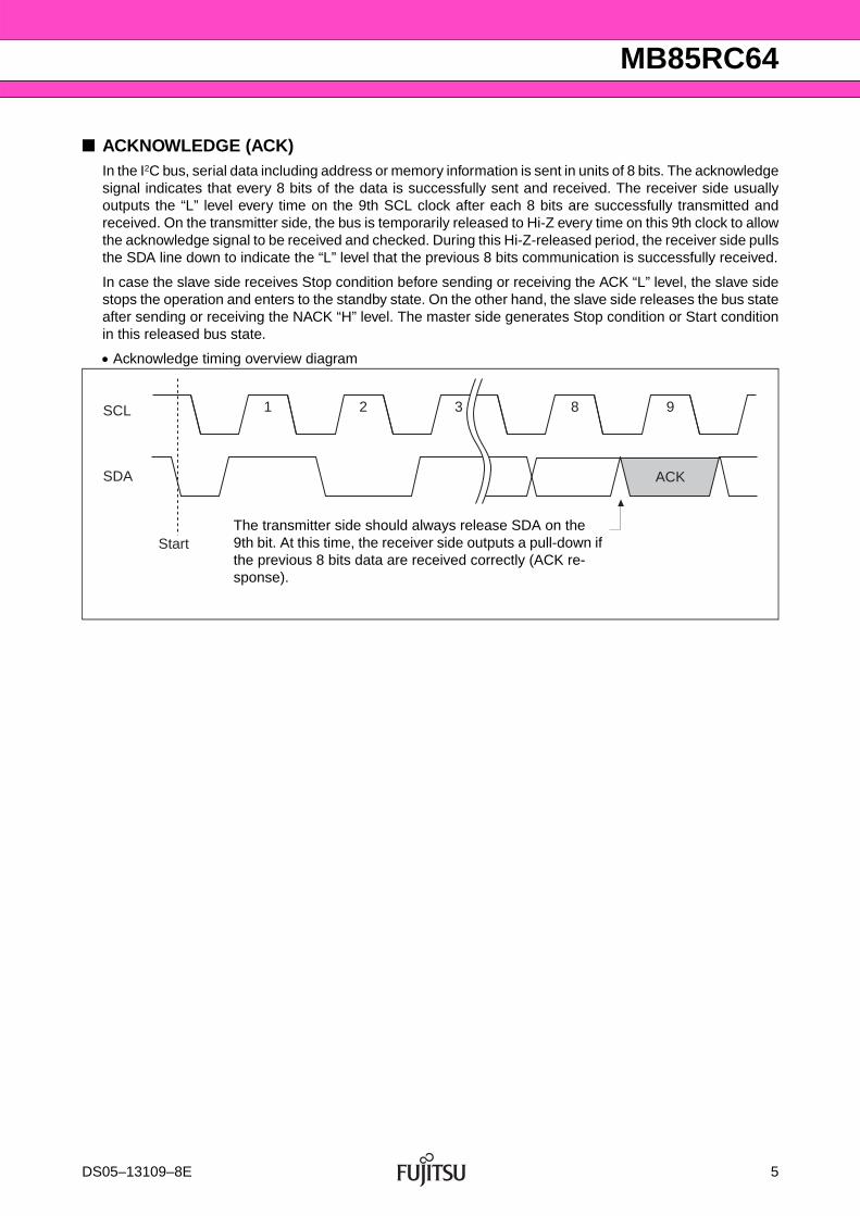
■ ACKNOWLEDGE (ACK)In the I2C bus, serial data including address or memory information is sent in units of 8 bits. The acknowledgesignal indicates that every 8 bits of the data is successfully sent and received. The receiver side usuallyoutputs the “L” level every time on the 9th SCL clock after each 8 bits are successfully transmitted andreceived. On the transmitter side, the bus is temporarily released to Hi-Z every time on this 9th clock to allowthe acknowledge signal to be received and checked. During this Hi-Z-released period, the receiver side pullsthe SDA line down to indicate the “L” level that the previous 8 bits communication is successfully received.
In case the slave side receives Stop condition before sending or receiving the ACK “L” level, the slave sidestops the operation and enters to the standby state. On the other hand, the slave side releases the bus stateafter sending or receiving the NACK “H” level. The master side generates Stop condition or Start conditionin this released bus state.
Acknowledge timing overview diagram
SCL 1 2 3 8 9
SDA
Start
ACK
The transmitter side should always release SDA on the 9th bit. At this time, the receiver side outputs a pull-down if the previous 8 bits data are received correctly (ACK re-sponse).
DS05–13109–8E 5
MB85RC64
■ DEVICE ADDRESS WORD (Slave address) Following the start condition, the master sends the 8 bits device address word to start I2C communication.The device address word (8 bits) consists of a device Type code (4 bits), device address code (3 bits), anda read/write code (1 bit).
• Device Type Code (4 bits)
The upper 4 bits of the device address word are a device type code that identifies the device type, and arefixed at “1010” for the MB85RC64.
• Device Address Code (3 bits)
Following the device type code, the 3 bits of the device address code are input in order of A2, A1, and A0.The device address code identifies one device from up to eight devices connected to the bus. Each MB85RC64 is given a unique 3 bits code on the device address pin (external hardware pin A2, A1,and A0). The slave only responds if the received device address code is equal to this unique 3 bits code.
• Read/Write Code (1 bit)
The 8th bit of the device address word is the R/W (read/write) code. When the R/W code is “0”, a writeoperation is enabled, and the R/W code is “1”, a read operation is enabled for the MB85RC64.
It turns to a stand-by state if the device code is not “1010” or device address code does not equal to pinsA2, A1, and A0.
Device Address Word
. .
. .
Start
ACK (SDA is the "L" level)
1 2 3 4 5 6 7 8 9 1 2
SCL
SDA ACK
Start Condition
Device Code Device Address Code Read/Write Code
A
S
S 1 0 1 0 A2 A1 A0 R/W A
Access from master
Access from slave
6 DS05–13109–8E
MB85RC64
■ DATA STRUCTUREIn the I2C bus, the acknowledge “L” level is output on the 9th bit by a slave, after the 8 bits of the deviceaddress word following the start condition are input by a master. After confirming the acknowledge responseby the master, the master outputs 8bits 2 memory address to the slave. When the each memory addressinput ends, the slave again outputs the acknowledge “L” level. After this operation, the I/O data follows inunits of 8 bits, with the acknowledge “L” level output after every 8 bits.
It is determined by the R/W code whether the data line is driven by the master or the slave. However, theclock line shall be driven by the master. For a write operation, the slave will accept 8 bits from the master,then send an acknowledge. If the master detects the acknowledge, the master will transfer the next 8 bits.For a read operation, the slave will place 8 bits on the data line, then wait for an acknowledge from the master.
■ FRAM ACKNOWLEDGE -- POLLING NOT REQUIREDThe MB85RC64 performs write operations at the same speed as read operations, so any waiting time foran ACK polling* does not occur. The write cycle takes no additional time.
*: In E2PROM, the Acknowledge Polling is performed as a progress check whether rewriting is executed or not.It is normal to judge by the 9th bit of Acknowledge whether rewriting is performed or not after inputting the start condition and then the device address word (8 bits) during rewriting.
■ WRITE PROTECT (WP) The entire memory array can be write protected using the Write Protect pin. When the Write Protect pin isset to the “H” level, the entire memory array will be write protected. When the Write Protect pin is the “L”level, entire memory array will be rewritten. Reading is allowed regardless of the WP pin's “H” level or “L” level.
Note : The Write Protect pin is pulled down internally to VSS pin, therefore if the Write Protect pin is open, the pin status is detected as the “L” level (write enabled).
DS05–13109–8E 7
MB85RC64
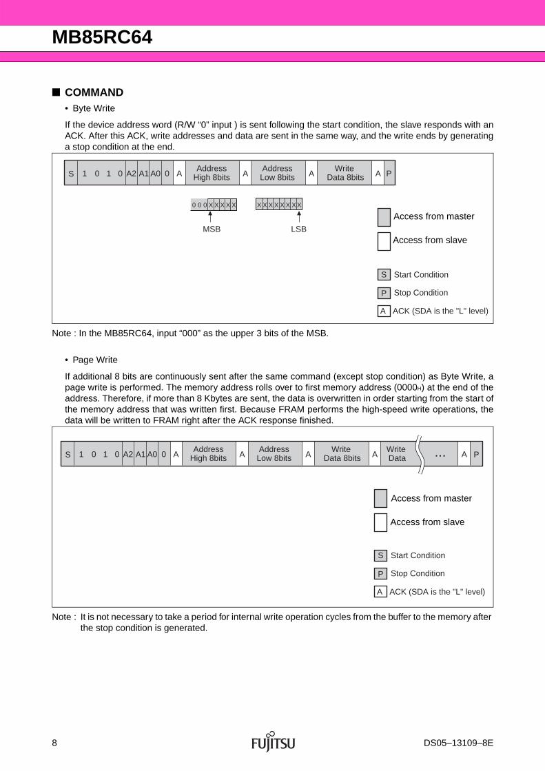
■ COMMAND• Byte Write
If the device address word (R/W “0” input ) is sent following the start condition, the slave responds with anACK. After this ACK, write addresses and data are sent in the same way, and the write ends by generatinga stop condition at the end.
Note : In the MB85RC64, input “000” as the upper 3 bits of the MSB.
• Page Write
If additional 8 bits are continuously sent after the same command (except stop condition) as Byte Write, apage write is performed. The memory address rolls over to first memory address (0000H) at the end of theaddress. Therefore, if more than 8 Kbytes are sent, the data is overwritten in order starting from the start ofthe memory address that was written first. Because FRAM performs the high-speed write operations, thedata will be written to FRAM right after the ACK response finished.
Note : It is not necessary to take a period for internal write operation cycles from the buffer to the memory after the stop condition is generated.
LSB
Start Condition
Stop Condition
ACK (SDA is the "L" level)A
S
P
MSB
0 0 0 X X X X X X X X X X X X X
S A2 A1 A0 A A A A PAddress
High 8bitsAddressLow 8bits
Write Data 8bits01 0 1 0
Access from master
Access from slave
Start Condition
Stop Condition
ACK (SDA is the "L" level)A
S
P
S A2 A1 A0 A A A A A PAddress
High 8bitsAddressLow 8bits
Write Data 8bits
Write Data ...01 0 1 0
Access from master
Access from slave
8 DS05–13109–8E
MB85RC64
• Current Address Read
When the previous write or read operation finishes successfully up to the stop condition and assumes thelast accessed address is “n”, then the address at “n+1” is read by sending the following command unlessturning the power off. If the memory address is last address, the address counter will roll over to 0000H. Thecurrent address in memory address buffer is undefined immediately after the power is turned on.
• Random Read
The one byte of data from the memory address saved in the memory address buffer can be read outsynchronously to SCL by specifying the address in the same way as for a write, and then issuing anotherstart condition and sending the Device Address Word (R/W “1” input).
The final NACK is issued by the receiver that receives the data. In this case, this bit is issued by the masterside.
Start Condition
Stop Condition
ACK(SDA is the "L" level)A
S
P
NACK (SDA is the "H" level)N
S A2 A1 A0 A N PRead
Data 8bits
(n+1) address
11 0 1 0
Access from master
Access from slave
Start Condition
Stop Condition
ACK (SDA is the "L" level)A
S
P
NACK (SDA is the "H" level)N
S A2 A1 A0 A A A PAddress
High 8bitsAddressLow 8bits01 0 1 0 S A2 A1 A0 A11 0 1 0
Read Data 8bits N
Access from master
Access from slave
DS05–13109–8E 9
MB85RC64
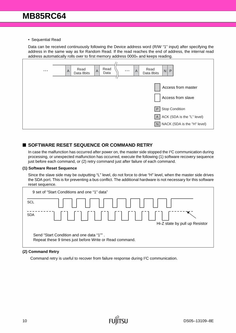
• Sequential Read
Data can be received continuously following the Device address word (R/W “1” input) after specifying theaddress in the same way as for Random Read. If the read reaches the end of address, the internal readaddress automatically rolls over to first memory address 0000H and keeps reading.
■ SOFTWARE RESET SEQUENCE OR COMMAND RETRYIn case the malfunction has occurred after power on, the master side stopped the I2C communication duringprocessing, or unexpected malfunction has occurred, execute the following (1) software recovery sequencejust before each command, or (2) retry command just after failure of each command.
(1) Software Reset Sequence
Since the slave side may be outputting “L” level, do not force to drive “H” level, when the master side drivesthe SDA port. This is for preventing a bus conflict. The additional hardware is not necessary for this softwarereset sequence.
(2) Command Retry
Command retry is useful to recover from failure response during I2C communication.
Stop Condition
ACK (SDA is the "L" level)A
P
NACK (SDA is the "H" level)N
A A A N PRead Data 8bits
Read Data 8bits
ReadData
......
Access from master
Access from slave
SCL
SDA
9 set of “Start Conditions and one “1” data”
Send “Start Condition and one data “1”” .Repeat these 9 times just before Write or Read command.
Hi-Z state by pull up Resistor
10 DS05–13109–8E
MB85RC64
■ ABSOLUTE MAXIMUM RATINGS
*: These parameters are based on the condition that VSS is 0 V.
WARNING: Semiconductor devices can be permanently damaged by application of stress (voltage, current, temperature, etc.) in excess of absolute maximum ratings. Do not exceed these ratings.
■ RECOMMENDED OPERATING CONDITIONS
*: These parameters are based on the condition that VSS is 0 V.
WARNING: The recommended operating conditions are required in order to ensure the normal operation of the semiconductor device. All of the device's electrical characteristics are warranted when the device is operated within these ranges.
Always use semiconductor devices within their recommended operating condition ranges. Operation outside these ranges may adversely affect reliability and could result in device failure.No warranty is made with respect to uses, operating conditions, or combinations not represented on the data sheet. Users considering application outside the listed conditions are advised to contact their representatives beforehand.
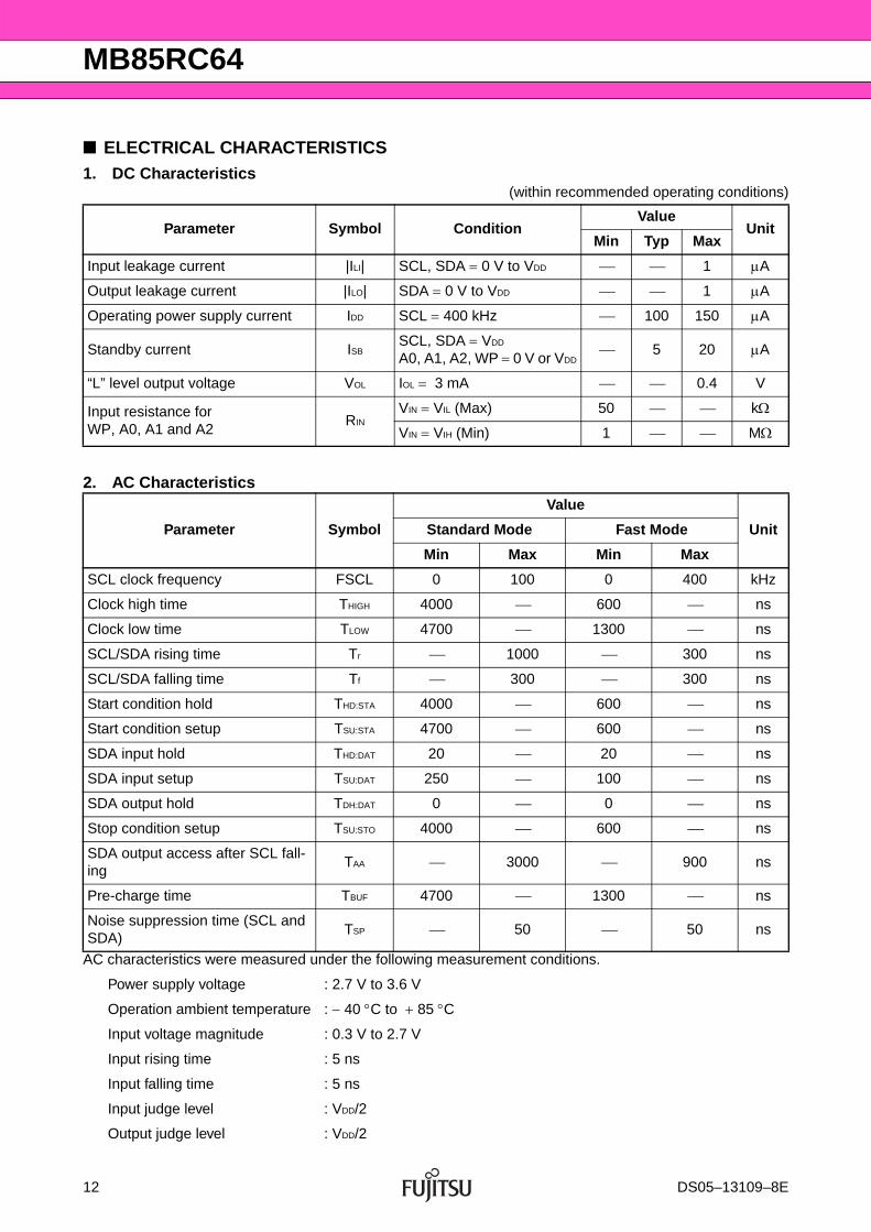
AC characteristics were measured under the following measurement conditions.
Power supply voltage : 2.7 V to 3.6 V
Operation ambient temperature : 40 C to 85 C
Input voltage magnitude : 0.3 V to 2.7 V
Input rising time : 5 ns
Input falling time : 5 ns
Input judge level : VDD/2
Output judge level : VDD/2
Parameter Symbol ConditionValue
UnitMin Typ Max
Input leakage current |ILI| SCL, SDA 0 V to VDD 1 A
Output leakage current |ILO| SDA 0 V to VDD 1 A
Operating power supply current IDD SCL 400 kHz 100 150 A
Standby current ISBSCL, SDA VDD
A0, A1, A2, WP 0 V or VDD 5 20 A
“L” level output voltage VOL IOL 3 mA 0.4 V
Input resistance for WP, A0, A1 and A2
RINVIN VIL (Max) 50 k
VIN VIH (Min) 1 M
Parameter Symbol
Value
UnitStandard Mode Fast Mode
Min Max Min Max
SCL clock frequency FSCL 0 100 0 400 kHz
Clock high time THIGH 4000 600 ns
Clock low time TLOW 4700 1300 ns
SCL/SDA rising time Tr 1000 300 ns
SCL/SDA falling time Tf 300 300 ns
Start condition hold THD:STA 4000 600 ns
Start condition setup TSU:STA 4700 600 ns
SDA input hold THD:DAT 20 20 ns
SDA input setup TSU:DAT 250 100 ns
SDA output hold TDH:DAT 0 0 ns
Stop condition setup TSU:STO 4000 600 ns
SDA output access after SCL fall-ing
TAA 3000 900 ns
Pre-charge time TBUF 4700 1300 ns
Noise suppression time (SCL and SDA)
TSP 50 50 ns
12 DS05–13109–8E
MB85RC64
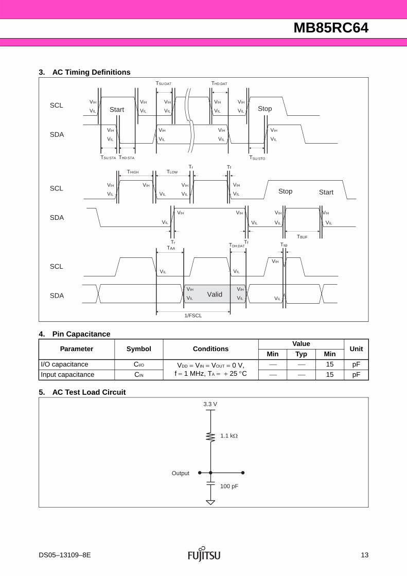
3. AC Timing Definitions
4. Pin Capacitance
5. AC Test Load Circuit
Parameter Symbol ConditionsValue
UnitMin Typ Min
I/O capacitance CI/O VDD VIN VOUT 0 V, f 1 MHz, TA 25 C
15 pF
Input capacitance CIN 15 pF
Start
StartStop
Stop
Valid
SCL
SDA
SCL
SDA
SCL
SDA
VIH
VIL
VIH
VIL
VIH
VIL
VIH
VIL
VIH
VIL
VIH
VIL
VIH
VIL
VIH
VIL
VIH
VIL
VIH
VIL
VIH
VIL
VIH
VIL
VIH
VIL
VIH
VIL
VIH
VIH VIH
TSU:DAT
TSU:STA THD:STA
THIGH TLOW
TDH:DAT
1/FSCL
TSU:STO
THD:DAT
VIH
VIH
VIH
VIL
VIL
VIL
VIL
VIL
VIL
VIL VIL
TBUFTfTr
TfTr
TAATsp
3.3 V
100 pF
Output
1.1 kΩ
DS05–13109–8E 13
MB85RC64
■ POWER ON/OFF SEQUENCEIf VDD falls down below 2.0V, VDD is required to be started from 0V to prevent malfunctions when the power is turned on again.
If the device does not operate within the specified conditions of read cycle, write cycle or power on/offsequence, memory data can not be guaranteed.
■ FRAM CHARACTERISTICS
*1 : Total number of reading and writing defines the minimum value of endurance, as an FRAM memory operates with destructive readout mechanism.
*2 : Minimun values define retention time of the first reading/writing data right after shipment, and these values are calculated by qualification results.
■ NOTE ON USE• Data written before performing IR reflow is not guaranteed after IR reflow. • During the access period from the start condition to the stop condition, keep the level of WP, A0, A1, and
A2 pins to the “H” level or the “L” level.
Parameter SymbolValue
UnitMin Max
SDA, SCL level hold time during power down tpd 85 ns
SDA, SCL level hold time during power up tpu 85 ns
Power supply rising time tr 10 s
Item Min Max Unit Parameter
Read/Write Endurance*1 1012 Times/byte Operation Ambient Temperature TA 85 C
Data Retention*2
10
Years
Operation Ambient Temperature TA 85 C
95 Operation Ambient Temperature TA 55 C
200 Operation Ambient Temperature TA 35 C
0 V
SDA, SCL >VDD × 0.8 * SDA, SCL >VDD × 0.8 *
tpd tputr
VIL (Max)
1.0 V
VIH (Min)
2.7 V
VDD
SDA, SCL : Don't careSDA, SCL SDA, SCL
0 V
VIL (Max)
1.0 V
VIH (Min)
2.7 V
VDD
* : SDA, SCL (Max) < VDD 0.5 V
14 DS05–13109–8E
MB85RC64
■ ESD AND LATCH-UP
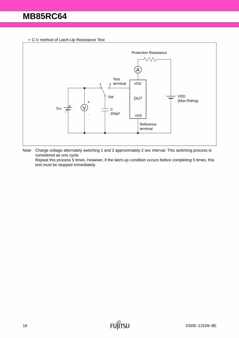
• Current method of Latch-Up Resistance Test
Note : The voltage VIN is increased gradually and the current IIN of 300 mA at maximum shall flow. Confirm the latch up does not occur under IIN 300 mA.In case the specific requirement is specified for I/O and IIN cannot be 300 mA, the voltage shall be increased to the level that meets the specific requirement.
Note Charge voltage alternately switching 1 and 2 approximately 2 sec interval. This switching process is considered as one cycle. Repeat this process 5 times. However, if the latch-up condition occurs before completing 5 times, this test must be stopped immediately.
VDD
VSS
DUT
VIN
+
-
SW
1 2
C200pF
V
A
Test terminal
Protection Resistance
VDD(Max.Rating)
Reference terminal
16 DS05–13109–8E
MB85RC64
■ REFLOW CONDITIONS AND FLOOR LIFE
Reflow Profile
Item Condition
Method IR (infrared reflow) , Convection
Times 2
Floor life
Before unpacking Please use within 2 years after production.
From unpacking to 2nd reflow Within 8 days
In case over period of floor life
Baking with 125 C+/-3 C for 24hrs+2hrs/-0hrs is required.
Then please use within 8 days. (Please remember baking is up to 2 times)
Floor life conditionBetween 5 C and 30 C and also below 70%RH required. (It is preferred lower humidity in the required temp range.)
260°C
(e)
(d')
(d)
255°C
170 °C
190 °C
RT (b)
(a)
(c)
to
Note : Temperature on the top of the package body is measured.
(a) Average ramp-up rate : 1 C/s to 4 C/s (b) Preheat & Soak : 170 C to 190 C, 60 s to 180 s (c) Average ramp-up rate : 1 C/s to 4 C/s (d) Peak temperature : Temperature 260 C Max; 255 C within 10 s (d’) Liquidous temperature : Up to 230 C within 40 s or
Up to 225 C within 60 s or Up to 220 C within 80 s
(e) Cooling : Natural cooling or forced cooling
Liquidous Temperature
DS05–13109–8E 17
MB85RC64
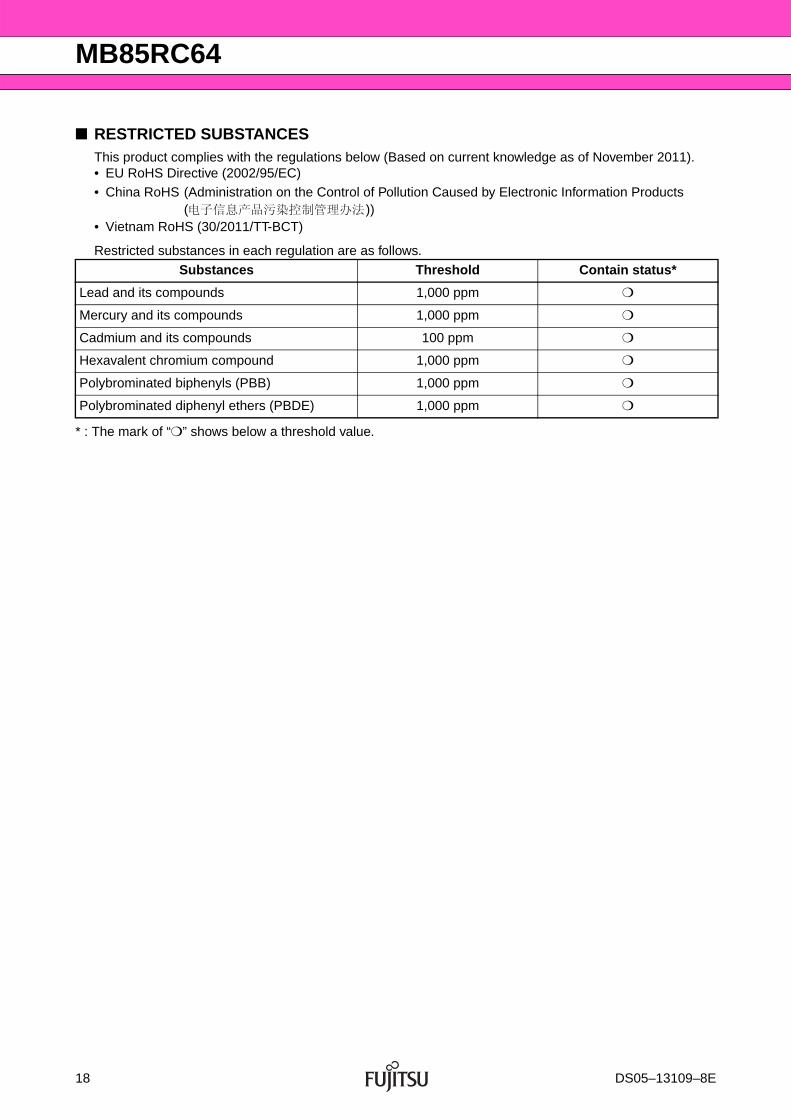
■ RESTRICTED SUBSTANCESThis product complies with the regulations below (Based on current knowledge as of November 2011).• EU RoHS Directive (2002/95/EC)• China RoHS (Administration on the Control of Pollution Caused by Electronic Information Products
( ))• Vietnam RoHS (30/2011/TT-BCT)
Restricted substances in each regulation are as follows.
* : The mark of “❍” shows below a threshold value.
Substances Threshold Contain status*
Lead and its compounds 1,000 ppm ❍
Mercury and its compounds 1,000 ppm ❍
Cadmium and its compounds 100 ppm ❍
Hexavalent chromium compound 1,000 ppm ❍
Polybrominated biphenyls (PBB) 1,000 ppm ❍
Polybrominated diphenyl ethers (PBDE) 1,000 ppm ❍
18 DS05–13109–8E
MB85RC64
■ ORDERING INFORMATION
Part number Package Shipping form Minimum shipping quantity
MB85RC64PNF-G-JNE1 8-pin, plastic SOP
(FPT-8P-M02)Tube 1
MB85RC64PNF-G-JNERE1 8-pin, plastic SOP
(FPT-8P-M02)Embossed Carrier tape 1500
DS05–13109–8E 19
MB85RC64
■ PACKAGE DIMENSION
Please check the latest package dimension at the following URL.http://edevice.fujitsu.com/package/en-search/
8-pin plastic SOP Lead pitch 1.27 mm
Package width × package length
3.9 mm × 5.05 mm
Lead shape Gullwing
Sealing method Plastic mold
Mounting height 1.75 mm MAX
Weight 0.06 g
8-pin plastic SOP(FPT-8P-M02)
(FPT-8P-M02)
C
1.27(.050)
3.90±0.30 6.00±0.20
.199 –.008+.010
–0.20+0.25
5.05
0.13(.005) M
(.154±.012) (.236±.008)
0.10(.004)
1 4
58
0.44±0.08(.017±.003)
–0.07+0.03
0.22
.009+.001–.003
45°
0.40(.016)
"A" 0~8°
0.25(.010)
(Mounting height)
Details of "A" part
1.55±0.20(.061±.008)
0.50±0.20(.020±.008)0.60±0.15
(.024±.006)
0.15±0.10(.006±.004)(Stand off)
0.10(.004)
*1
*2
2002-2012 FUJITSU SEMICONDUCTOR LIMITED F08004S-c-5-10Dimensions in mm (inches).Note: The values in parentheses are reference values.
Note 1) 1 : These dimensions include resin protrusion.Note 2) 2 : These dimensions do not include resin protrusion.Note 3) Pins width and pins thickness include plating thickness.Note 4) Pins width do not include tie bar cutting remainder.
**
20 DS05–13109–8E
MB85RC64
■ MARKING
RC64E11000
300
[MB85RC64PNF-G-JNE1][MB85RC64PNF-G-JNERE1]
[FPT-8P-M02]
DS05–13109–8E 21
MB85RC64
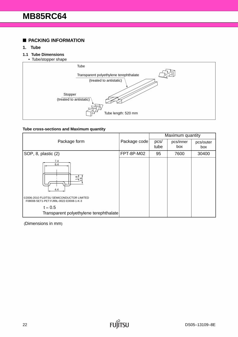
■ PACKING INFORMATION1. Tube
1.1 Tube Dimensions• Tube/stopper shape
Tube cross-sections and Maximum quantity
Package form Package codeMaximum quantity
pcs/tube
pcs/inner box
pcs/outer box
SOP, 8, plastic (2)
t 0.5 Transparent polyethylene terephthalate
FPT-8P-M02 95 7600 30400
(Dimensions in mm)
(treated to antistatic)
Tube length: 520 mm
(treated to antistatic) Stopper
Tube
Transparent polyethylene terephthalate
4.4
6.47.4
1.8
C 2006 FUJITSU LIMITED F08008-SET1-PET:FJ99L-0022-E0008-1-K-1
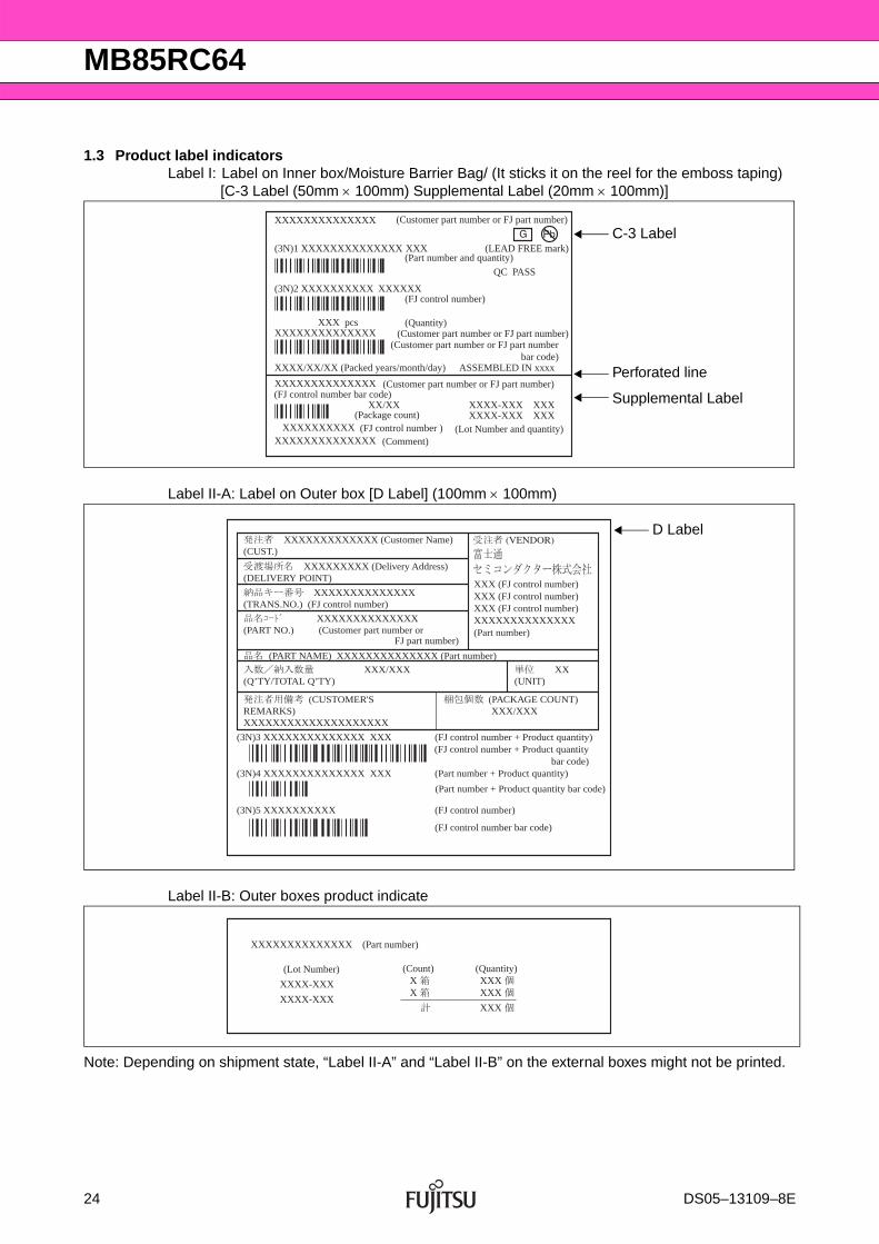
Label II-A: Label on Outer box [D Label] (100mm 100mm)
Label II-B: Outer boxes product indicate
Note: Depending on shipment state, “Label II-A” and “Label II-B” on the external boxes might not be printed.
(Customer part number or FJ part number)
(Customer part number or FJ part number)
(FJ control number bar code)XX/XX XXXX-XXX XXX
XXXX-XXX XXX(Lot Number and quantity)
(Package count)
(Customer part number or FJ part numberbar code)
(Part number and quantity)
(FJ control number)
QC PASS
XXXXXXXXXXXXXX
XXXX/XX/XX (Packed years/month/day) ASSEMBLED IN xxxx
(3N)1 XXXXXXXXXXXXXX XXX
(Quantity)
(3N)2 XXXXXXXXXX
XXX pcs
XXXXXX
XXXXXXXXXXXXXX
(Customer part number or FJ part number)XXXXXXXXXXXXXX
(Comment)XXXXXXXXXXXXXX(FJ control number )XXXXXXXXXX
(LEAD FREE mark)C-3 Label
Supplemental Label
Perforated line
XXXXXXXXXXXXX (Customer Name)(CUST.)
XXX (FJ control number)XXX (FJ control number)XXX (FJ control number)XXXXXXXXXXXXXX(Part number)
(FJ control number + Product quantity)(FJ control number + Product quantity
bar code)
(Part number + Product quantity bar code)
XXXXXXXXX (Delivery Address)(DELIVERY POINT)
XXXXXXXXXXXXXX(TRANS.NO.) (FJ control number)
XXXXXXXXXXXXXX(PART NO.) (Customer part number or
FJ part number)
XXX/XXX(Q’TY/TOTAL Q’TY)
XX(UNIT)
(CUSTOMER'S REMARKS)XXXXXXXXXXXXXXXXXXXX
(PACKAGE COUNT) XXX/XXX
(PART NAME) XXXXXXXXXXXXXX (Part number)
(3N)3 XXXXXXXXXXXXXX XXX
(Part number + Product quantity)(3N)4 XXXXXXXXXXXXXX XXX
(FJ control number)
(FJ control number bar code)
(3N)5 XXXXXXXXXX
D Label
XXXXXXXXXXXXXX (Part number)
(Lot Number)
XXXX-XXX
XXXX-XXX
(Count) (Quantity) X XXX X XXX
XXX
DS05–13109–8E 29
MB85RC64
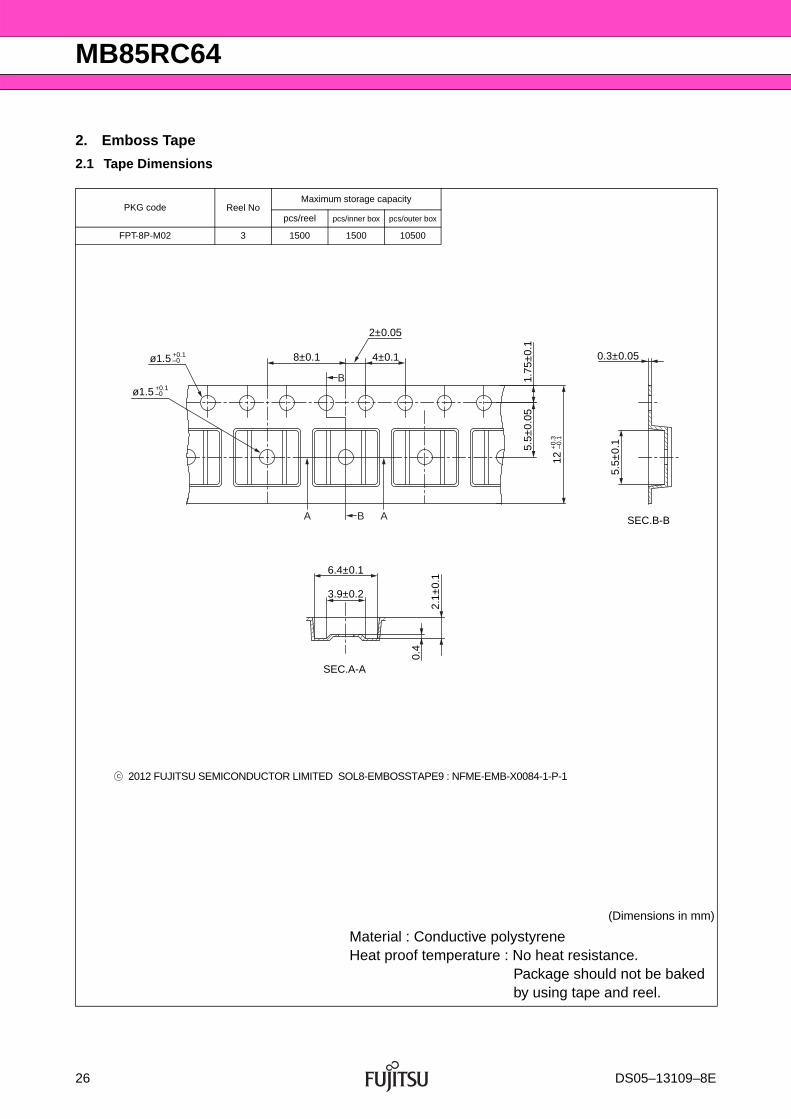
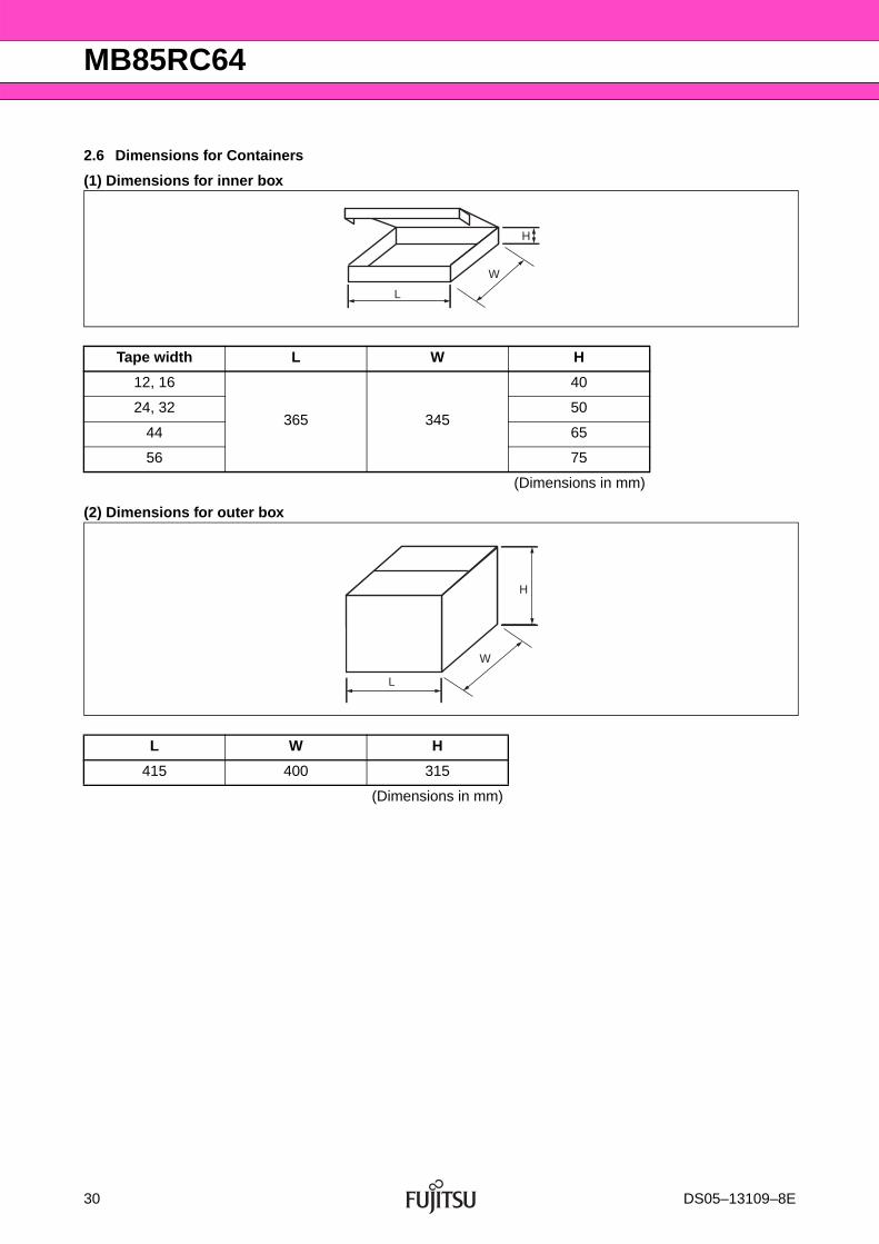
2.6 Dimensions for Containers
(1) Dimensions for inner box
(2) Dimensions for outer box
Tape width L W H
12, 16
365 345
40
24, 32 50
44 65
56 75
(Dimensions in mm)
L W H
415 400 315
(Dimensions in mm)
L
W
H
L
W
H
30 DS05–13109–8E
MB85RC64
■ MAJOR CHANGES IN THIS EDITIONA change on a page is indicated by a vertical line drawn on the left side of that page.
Page Section Change Results
1
■ FEATURES Revised the Data retention10 years ( 85 C)10 years ( 85 C), 95 years ( 55 C),
over 200 years ( 35 C)
11■ ABSOLUTE MAXIMUM RATINGS Revised the Storage Temperature
40 C 55 C
14
■ POWER ON/OFF SEQUENCE Revised the following description:“POWER ON SEQUENCE” “POWER ON/OFF SEQUENCE”
Added the following description: “If the device does not operate within the specified conditions of read cycle, write cycle or power on/off sequence, memory data can not be guaranteed.”
Revised the following description:“VDD pin is required to be rising from 0 V because turning the power on from an intermediate level may cause malfunctions, when the power is turned on”“If VDD falls down below 2.0V, VDD is required to be started from 0V to prevent malfunctions when the power is turned on again.”
North and South AmericaFUJITSU SEMICONDUCTOR AMERICA, INC.1250 E. Arques Avenue, M/S 333Sunnyvale, CA 94085-5401, U.S.A.Tel: +1-408-737-5600 Fax: +1-408-737-5999http://us.fujitsu.com/micro/
KoreaFUJITSU SEMICONDUCTOR KOREA LTD.902 Kosmo Tower Building, 1002 Daechi-Dong,Gangnam-Gu, Seoul 135-280, Republic of KoreaTel: +82-2-3484-7100 Fax: +82-2-3484-7111http://kr.fujitsu.com/fsk/
Asia PacificFUJITSU SEMICONDUCTOR ASIA PTE. LTD.151 Lorong Chuan,#05-08 New Tech Park 556741 SingaporeTel : +65-6281-0770 Fax : +65-6281-0220http://sg.fujitsu.com/semiconductor/
FUJITSU SEMICONDUCTOR PACIFIC ASIA LTD.2/F, Green 18 Building, Hong Kong Science Park,Shatin, N.T., Hong KongTel : +852-2736-3232 Fax : +852-2314-4207http://cn.fujitsu.com/fsp/
Specifications are subject to change without notice. For further information please contact each office.
All Rights Reserved.The contents of this document are subject to change without notice. Customers are advised to consult with sales representatives before ordering.The information, such as descriptions of function and application circuit examples, in this document are presented solely for the purposeof reference to show examples of operations and uses of FUJITSU SEMICONDUCTOR device; FUJITSU SEMICONDUCTOR doesnot warrant proper operation of the device with respect to use based on such information. When you develop equipment incorporatingthe device based on such information, you must assume any responsibility arising out of such use of the information. FUJITSU SEMICONDUCTOR assumes no liability for any damages whatsoever arising out of the use of the information.Any information in this document, including descriptions of function and schematic diagrams, shall not be construed as license of the useor exercise of any intellectual property right, such as patent right or copyright, or any other right of FUJITSU SEMICONDUCTOR or anythird party or does FUJITSU SEMICONDUCTOR warrant non-infringement of any third-party's intellectual property right or other rightby using such information. FUJITSU SEMICONDUCTOR assumes no liability for any infringement of the intellectual property rights orother rights of third parties which would result from the use of information contained herein.The products described in this document are designed, developed and manufactured as contemplated for general use, including withoutlimitation, ordinary industrial use, general office use, personal use, and household use, but are not designed, developed and manufacturedas contemplated (1) for use accompanying fatal risks or dangers that, unless extremely high safety is secured, could have a serious effectto the public, and could lead directly to death, personal injury, severe physical damage or other loss (i.e., nuclear reaction control innuclear facility, aircraft flight control, air traffic control, mass transport control, medical life support system, missile launch control inweapon system), or (2) for use requiring extremely high reliability (i.e., submersible repeater and artificial satellite).Please note that FUJITSU SEMICONDUCTOR will not be liable against you and/or any third party for any claims or damages aris-ing in connection with above-mentioned uses of the products.Any semiconductor devices have an inherent chance of failure. You must protect against injury, damage or loss from such failuresby incorporating safety design measures into your facility and equipment such as redundancy, fire protection, and prevention of over-current levels and other abnormal operating conditions.Exportation/release of any products described in this document may require necessary procedures in accordance with the regulationsof the Foreign Exchange and Foreign Trade Control Law of Japan and/or US export control laws.The company names and brand names herein are the trademarks or registered trademarks of their respective owners.