Page 1
Hier wird Wissen Wirklichkeit Computer Architecture – Part 11 – page 1 of 44 – Prof. Dr. Uwe Brinkschulte, Prof. Dr. Klaus Waldschmidt
Part 13
Memory management, Many-Cores (CMP),and Crossbars
Computer Architecture
Slide Sets
WS 2012/2013
Prof. Dr. Uwe BrinkschulteM.Sc. Benjamin Betting
Page 2
Hier wird Wissen Wirklichkeit Computer Architecture – Part 11 – page 2 of 44 – Prof. Dr. Uwe Brinkschulte, Prof. Dr. Klaus Waldschmidt
Chip-Multiprocessors (CMP)/Multi-/Many-Cores
Possible Classification?
Page 3
Hier wird Wissen Wirklichkeit Computer Architecture – Part 11 – page 3 of 44 – Prof. Dr. Uwe Brinkschulte, Prof. Dr. Klaus Waldschmidt
Processor Parameters (< 2005)
Page 4
Hier wird Wissen Wirklichkeit Computer Architecture – Part 11 – page 4 of 44 – Prof. Dr. Uwe Brinkschulte, Prof. Dr. Klaus Waldschmidt
CMT configurations (<2008)
Page 5
Hier wird Wissen Wirklichkeit Computer Architecture – Part 11 – page 5 of 44 – Prof. Dr. Uwe Brinkschulte, Prof. Dr. Klaus Waldschmidt
Sun UltraSPARC T1 (Niagara-1)
General:
• Server Chip-Multiprocessor (CMP)
• Developed by Sun Microsystems (2005)
• Extended to Niagara-2 (2008)
Goal:
Designed for high throughput and excellent performance/Watt on
server workloads
HSA:
• 8x scalar pipelined processing cores on the DIE
(32-bit SPARC, 4-way MT)
• L2-Cache coupling (UMA, DDR2 controllers)
Page 6
Hier wird Wissen Wirklichkeit Computer Architecture – Part 11 – page 6 of 44 – Prof. Dr. Uwe Brinkschulte, Prof. Dr. Klaus Waldschmidt
Niagara-1 Block Diagram
Page 7
Hier wird Wissen Wirklichkeit Computer Architecture – Part 11 – page 7 of 44 – Prof. Dr. Uwe Brinkschulte, Prof. Dr. Klaus Waldschmidt
Niagara-1 DIE (90nm process)
Page 8
Hier wird Wissen Wirklichkeit Computer Architecture – Part 11 – page 8 of 44 – Prof. Dr. Uwe Brinkschulte, Prof. Dr. Klaus Waldschmidt
Niagara-1 SPARC Core Pipeline
• six stages deep (shallow pipeline)
• low speculative (branch target buffer + precompute branch logic)
• single issue (IPC = 1.0)
• 4-way fine-grain multithreading (cycle-by-cycle interleaved + priority
LRU)
Page 9
Hier wird Wissen Wirklichkeit Computer Architecture – Part 11 – page 9 of 44 – Prof. Dr. Uwe Brinkschulte, Prof. Dr. Klaus Waldschmidt
• Switching between available threads each cycle with priority given
to the least recently used thread.
• Threads become available of long latency such as e.g., loads,
branches, multiply, and divide.
• Threads become unavailable of pipeline "stalls" e.g, cache misses,
traps, and resource conflicts
• Designed from ground up to 32-thread CMP
Multithreading on Niagara-1
Page 10
Hier wird Wissen Wirklichkeit Computer Architecture – Part 11 – page 10 of 44 – Prof. Dr. Uwe Brinkschulte, Prof. Dr. Klaus Waldschmidt
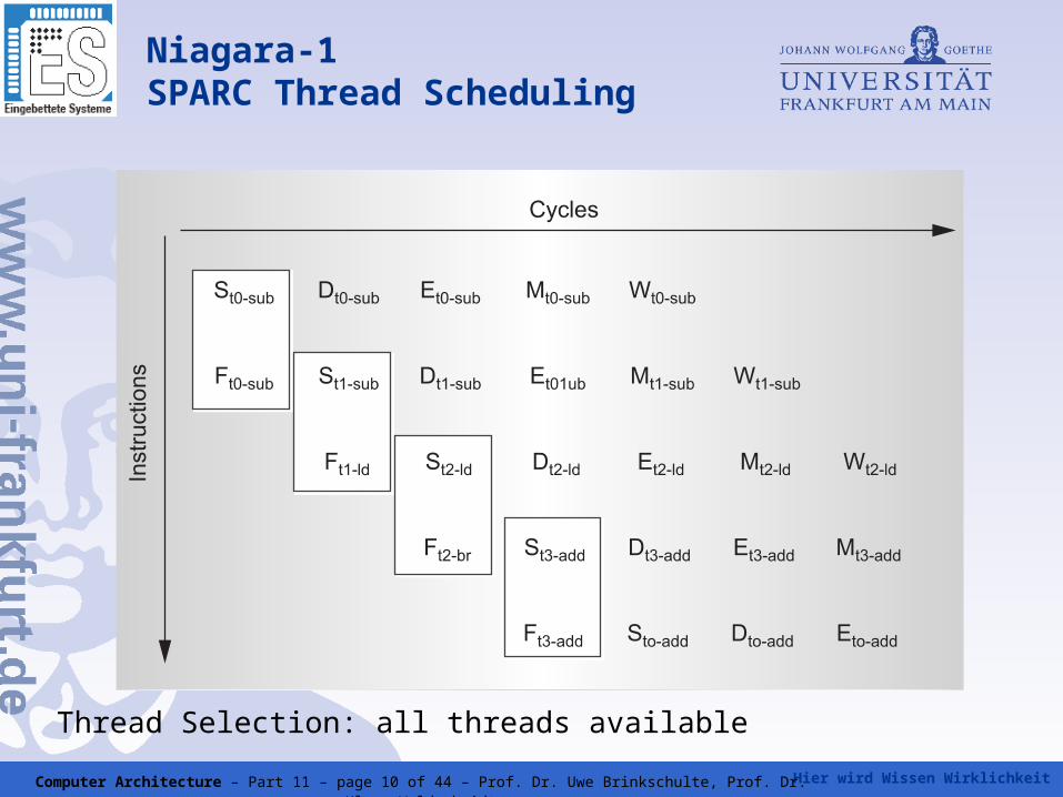
Thread Selection: all threads available
Niagara-1 SPARC Thread Scheduling
Page 11
Hier wird Wissen Wirklichkeit Computer Architecture – Part 11 – page 11 of 44 – Prof. Dr. Uwe Brinkschulte, Prof. Dr. Klaus Waldschmidt
There are 5 core components to consider when describing the
memory architecture of Niagara-1 processor:
1. SPARC pipelines (cores)
2. L1-Caches
3. L2-Caches
4. DRAM controller
5. IO Devices (out of scope)
Hint: 1. and 2. also consider the on-Chip interconnection network
between components e.g., buses, crossbars etc.
Memory Resources on Niagara-1
Page 12
Hier wird Wissen Wirklichkeit Computer Architecture – Part 11 – page 12 of 44 – Prof. Dr. Uwe Brinkschulte, Prof. Dr. Klaus Waldschmidt
L1-Caches
L1-Cache is contained exclusively for instructions (L1-I) and data
(L1-D) within each SPARC core and shared between the 4 threads
L1-I:
• 16 Kbyte, 4-way set-associative, block size of 32 bytes (line size)
• two instruction fetch each cycle (one speculative)
L1-D:
• 8 Kbyte, 4-way set-associative, block size of 16 bytes
• write-through policy, and 8-entry-store buffer (execution past
stores)small L1-Caches, 3 clocks latency for cache hit, and
miss rate in the range of 10%
Page 13
Hier wird Wissen Wirklichkeit Computer Architecture – Part 11 – page 13 of 44 – Prof. Dr. Uwe Brinkschulte, Prof. Dr. Klaus Waldschmidt
L1-Caches
Why to choose small L1-caches with 4-way set-associativity???
....Well, because commercial server applications tend to have large
working sets, the L1-Caches must be much larger to achieve
significantly lower miss rates,..........but the Niagara designers observed
that the incremental performance gained by larger caches did not merit the
area increase..............
....In Niagara, the four threads of each core are very effective at hiding
the latencies from L1 and L2 misses ..........Therefore, the smaller
Niagara level-one cache sizes are good tradeoff between miss rates, area
and the ability of other threads in the processor core to hide latency........
(by James Laudon, Sun Microsystems)
Page 14
Hier wird Wissen Wirklichkeit Computer Architecture – Part 11 – page 14 of 44 – Prof. Dr. Uwe Brinkschulte, Prof. Dr. Klaus Waldschmidt
L2-Caches
L2-Cache is contained single on-chip, commonly shared for
instructions and data, banked 4-ways and pipelined.
• 3 Mbytes total, 12-way set-associative, block size 64 bytes
• Banked across 4 L2-banks, interleaved at 64 byte granularity
• Bank selection: physical address bits [7:6]
• 23 clocks latency for L1-D cache miss, and 22 clocks for L1-I
• Cache coherency: full MESI based protocol between L1 and L2
• Line-replacement algorithm: some sort of LRU
Page 15
Hier wird Wissen Wirklichkeit Computer Architecture – Part 11 – page 15 of 44 – Prof. Dr. Uwe Brinkschulte, Prof. Dr. Klaus Waldschmidt
L2-Caches
Single Shared L2-Cache:
Advantage: A single shared on-chip cache eliminates cache
coherence misses in L2 and replaces them with
low latency shared communication between L1 and L2
Disadvantage: It also implies longer access time to the L2 because
the cache cannot be located close to all of the
processor cores in the chip. Furthermore, highly
frequented banks could lead to a bottleneck, too
Page 16
Hier wird Wissen Wirklichkeit Computer Architecture – Part 11 – page 16 of 44 – Prof. Dr. Uwe Brinkschulte, Prof. Dr. Klaus Waldschmidt
NxM Crossbar Interconnect
Purpose:
Niagara's crossbar interconnect provides and manages fast
communication link between processor cores, L2-Cache banks, and
other shared resources on the chip (e.g., FPU, IO-bridge etc.)
Reminder: What is a crossbar?
•None-blocking, NxM interconnecting network
•N Inputs, M Outputs (individual switches on each cross node)
•memory bandwith, up to several GB/s
Page 17
Hier wird Wissen Wirklichkeit Computer Architecture – Part 11 – page 17 of 44 – Prof. Dr. Uwe Brinkschulte, Prof. Dr. Klaus Waldschmidt
NxM Crossbar Example
Page 18
Hier wird Wissen Wirklichkeit
CCX contains two main blocks (one for each direction):
•Processor-Cache Crossbar (PCX), 8x5, Forward Crossbar
•Cache-Processor Crossbar (CPX), 6x8, Backward Crossbar
Computer Architecture – Part 11 – page 18 of 44 – Prof. Dr. Uwe Brinkschulte, Prof. Dr. Klaus Waldschmidt
Niagara-1 CPU Cache Crossbar (CCX)
Page 19
Hier wird Wissen Wirklichkeit Computer Architecture – Part 11 – page 19 of 44 – Prof. Dr. Uwe Brinkschulte, Prof. Dr. Klaus Waldschmidt
Niagara-1 Processor-Cache Crossbar (PCX)
• Accepts packets from a source (any of eight SPARC CPU cores) and delivers
the packet to its destination (any one of the four L2-Cache banks, the I/O
bridge, or the FPU)
• A source sends a packet and a destination ID to the PCX
• A packet is sent on a separate 124-bit wide parallel bus ( 40 bits address, 64
bits data, and rest for control)
• Destination ID is sent on a separate 5-bit parallel bus
• Each source connects with its own separate bus to the PCX
• PCX sends a grant to the source after dispatching a packet to its destination
(handshake signal)
• When a destination reaches its limit, it sends a stall signal to the PCX (exc. FPU)
8x buses that connect from the CPUs to the
PCX
Page 20
Hier wird Wissen Wirklichkeit Computer Architecture – Part 11 – page 20 of 44 – Prof. Dr. Uwe Brinkschulte, Prof. Dr. Klaus Waldschmidt
Niagara-1 PCX- Block Diagram
Page 21
Hier wird Wissen Wirklichkeit Computer Architecture – Part 11 – page 21 of 44 – Prof. Dr. Uwe Brinkschulte, Prof. Dr. Klaus Waldschmidt
Niagara-1 PCX-Issues
Advantage: None-blocking access, overall more than 200 Gbytes/s of
bandwidth
Problem: Bus collisions may occur when multiple sources send a
packet to the same destination
Solution: When multiple sources send a packet to the same
destination, the PCX buffers each packet and arbitrates
its delivery to the destination. The CCX does not modify
or process any packet
Extending PCX with arbitration (one for each
destination)
Page 22
Hier wird Wissen Wirklichkeit
• 5 identical arbiters with 16 entry deep FIFO-queues
(max. 2 entries per source)
• up to 96 queued transactions Computer Architecture – Part 11 – page 22 of 44 – Prof. Dr. Uwe Brinkschulte, Prof. Dr. Klaus Waldschmidt
Niagara-1 PCX - Arbiter Data Flow
Page 23
Hier wird Wissen Wirklichkeit Computer Architecture – Part 11 – page 23 of 44 – Prof. Dr. Uwe Brinkschulte, Prof. Dr. Klaus Waldschmidt
Niagara-1 Cache-Processor Crossbar (CPX)
• Opposed data transaction direction of PCX (Backward)
• 6 sources (L2-banks, FPU, and IO bridge) and 8 destinations (SPARC Cores)
• A packet is sent on a separate 145-bit wide parallel bus (128 bits data, and rest
for control)
• Destination ID is sent on a separate 8-bit parallel bus
• CPX sends a grant to the source after dispatching a packet to its destination
• Unlike the PCX, the CPX does not receive a stall from any of its destinations
• contains 8 identical arbiters with 8 queues and a two entry deep FIFO
6 buses that connect from the sources to the CPX
Page 24
Hier wird Wissen Wirklichkeit Computer Architecture – Part 11 – page 24 of 44 – Prof. Dr. Uwe Brinkschulte, Prof. Dr. Klaus Waldschmidt
Niagara-1 CPX - Block Diagram
Page 25
Hier wird Wissen Wirklichkeit Computer Architecture – Part 11 – page 25 of 44 – Prof. Dr. Uwe Brinkschulte, Prof. Dr. Klaus Waldschmidt
Superscalar vs. CMP
Page 26
Hier wird Wissen Wirklichkeit Computer Architecture – Part 11 – page 26 of 44 – Prof. Dr. Uwe Brinkschulte, Prof. Dr. Klaus Waldschmidt
IPC rates
Page 27
Hier wird Wissen Wirklichkeit
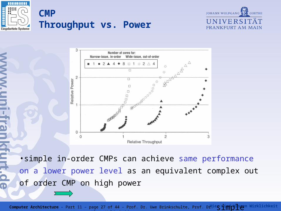
•simple in-order CMPs can achieve same performance on a lower
power level as an equivalent complex out of order CMP on high
power
simple CMPs gain better Watt/PerformanceComputer Architecture – Part 11 – page 27 of 44 – Prof. Dr. Uwe Brinkschulte, Prof. Dr. Klaus Waldschmidt
CMPThroughput vs. Power
Page 28
Hier wird Wissen Wirklichkeit Computer Architecture – Part 11 – page 28 of 44 – Prof. Dr. Uwe Brinkschulte, Prof. Dr. Klaus Waldschmidt
Niagara-1Heat Dissipation