184
Passive Circuit DesignGuide December 2003

Passive Circuit DesignGuide
December 2003

Notice
The information contained in this document is subject to change without notice.
Agilent Technologies makes no warranty of any kind with regard to this material,including, but not limited to, the implied warranties of merchantability and fitnessfor a particular purpose. Agilent Technologies shall not be liable for errors containedherein or for incidental or consequential damages in connection with the furnishing,performance, or use of this material.
Warranty
A copy of the specific warranty terms that apply to this software product is availableupon request from your Agilent Technologies representative.
Restricted Rights Legend
Use, duplication or disclosure by the U. S. Government is subject to restrictions as setforth in subparagraph (c) (1) (ii) of the Rights in Technical Data and ComputerSoftware clause at DFARS 252.227-7013 for DoD agencies, and subparagraphs (c) (1)and (c) (2) of the Commercial Computer Software Restricted Rights clause at FAR52.227-19 for other agencies.
Agilent Technologies395 Page Mill RoadPalo Alto, CA 94304 U.S.A.
Copyright © 1998-2003, Agilent Technologies. All Rights Reserved.
Acknowledgments
Mentor Graphics is a trademark of Mentor Graphics Corporation in the U.S. andother countries.
Microsoft®, Windows®, MS Windows®, Windows NT®, and MS-DOS® are U.S.registered trademarks of Microsoft Corporation.
Pentium® is a U.S. registered trademark of Intel Corporation.
PostScript® and Acrobat® are trademarks of Adobe Systems Incorporated.
UNIX® is a registered trademark of the Open Group.
ii
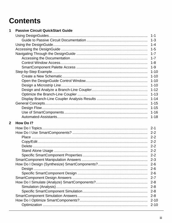
Contents1 Passive Circuit QuickStart Guide
Using DesignGuides................................................................................................. 1-1Guide to Passive Circuit Documentation ............................................................ 1-3
Using the DesignGuide............................................................................................. 1-4Accessing the DesignGuide ..................................................................................... 1-5Navigating Through the DesignGuide ...................................................................... 1-7
Accessing the Documentation............................................................................ 1-7Control Window Access...................................................................................... 1-8SmartComponent Palette Access ...................................................................... 1-9
Step-by-Step Example.............................................................................................. 1-10Create a New Schematic.................................................................................... 1-10Open the DesignGuide Control Window............................................................. 1-10Design a Microstrip Line..................................................................................... 1-10Design and Analyze a Branch-Line Coupler....................................................... 1-12Optimize the Branch-Line Coupler ..................................................................... 1-13Display Branch-Line Coupler Analysis Results .................................................. 1-14
General Concepts..................................................................................................... 1-15Design Flow........................................................................................................ 1-15Use of SmartComponents .................................................................................. 1-16Automated-Assistants......................................................................................... 1-18
2 How Do I?How Do I Topics........................................................................................................ 2-1How Do I Use SmartComponents? .......................................................................... 2-2
Place .................................................................................................................. 2-2Copy/Edit ............................................................................................................ 2-2Delete ................................................................................................................. 2-2Stand Alone Usage ............................................................................................ 2-2Specific SmartComponent Properties ................................................................ 2-2
SmartComponent Manipulation Answers ................................................................. 2-3How Do I Design (Synthesize) SmartComponents?................................................. 2-6
Design ................................................................................................................ 2-6Specific SmartComponent Design ..................................................................... 2-6
SmartComponent Design Answers .......................................................................... 2-7How Do I Simulate (Analyze) SmartComponents?................................................... 2-8
Simulation (Analysis) .......................................................................................... 2-8Specific SmartComponent Simulation................................................................ 2-8
SmartComponent Simulation Answers..................................................................... 2-8How Do I Optimize SmartComponents?................................................................... 2-10
Optimization ....................................................................................................... 2-10
iii
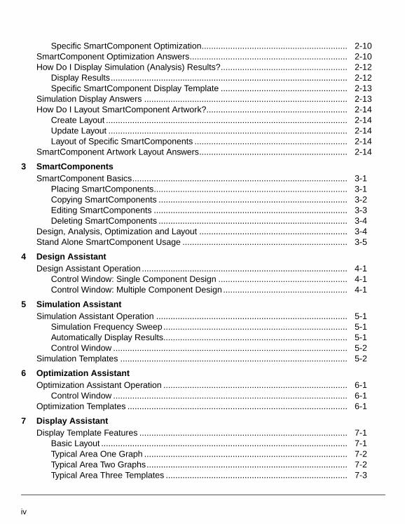
Specific SmartComponent Optimization............................................................. 2-10SmartComponent Optimization Answers.................................................................. 2-10How Do I Display Simulation (Analysis) Results?..................................................... 2-12
Display Results................................................................................................... 2-12Specific SmartComponent Display Template ..................................................... 2-13
Simulation Display Answers ..................................................................................... 2-13How Do I Layout SmartComponent Artwork?........................................................... 2-14
Create Layout ..................................................................................................... 2-14Update Layout .................................................................................................... 2-14Layout of Specific SmartComponents ................................................................ 2-14
SmartComponent Artwork Layout Answers.............................................................. 2-14
3 SmartComponentsSmartComponent Basics.......................................................................................... 3-1
Placing SmartComponents................................................................................. 3-1Copying SmartComponents ............................................................................... 3-2Editing SmartComponents ................................................................................. 3-3Deleting SmartComponents ............................................................................... 3-4
Design, Analysis, Optimization and Layout .............................................................. 3-4Stand Alone SmartComponent Usage ..................................................................... 3-5
4 Design AssistantDesign Assistant Operation ...................................................................................... 4-1
Control Window: Single Component Design ...................................................... 4-1Control Window: Multiple Component Design .................................................... 4-1
5 Simulation AssistantSimulation Assistant Operation ................................................................................ 5-1
Simulation Frequency Sweep............................................................................. 5-1Automatically Display Results............................................................................. 5-1Control Window .................................................................................................. 5-2
Simulation Templates ............................................................................................... 5-2
6 Optimization AssistantOptimization Assistant Operation ............................................................................. 6-1
Control Window .................................................................................................. 6-1Optimization Templates ............................................................................................ 6-1
7 Display AssistantDisplay Template Features ....................................................................................... 7-1
Basic Layout ....................................................................................................... 7-1Typical Area One Graph ..................................................................................... 7-2Typical Area Two Graphs.................................................................................... 7-2Typical Area Three Templates ............................................................................ 7-3
iv
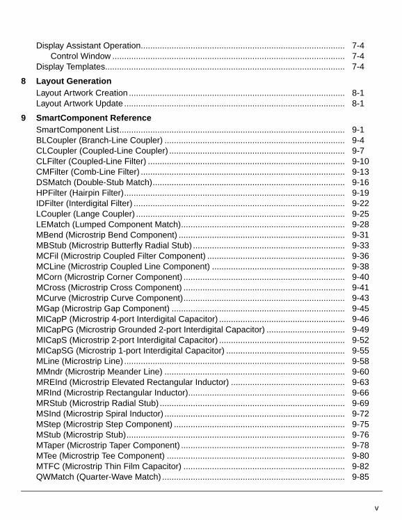
Display Assistant Operation...................................................................................... 7-4Control Window .................................................................................................. 7-4
Display Templates..................................................................................................... 7-4
8 Layout GenerationLayout Artwork Creation ........................................................................................... 8-1Layout Artwork Update ............................................................................................. 8-1
9 SmartComponent ReferenceSmartComponent List............................................................................................... 9-1BLCoupler (Branch-Line Coupler) ............................................................................ 9-4CLCoupler (Coupled-Line Coupler) .......................................................................... 9-7CLFilter (Coupled-Line Filter) ................................................................................... 9-10CMFilter (Comb-Line Filter) ...................................................................................... 9-13DSMatch (Double-Stub Match)................................................................................. 9-16HPFilter (Hairpin Filter)............................................................................................. 9-19IDFilter (Interdigital Filter) ......................................................................................... 9-22LCoupler (Lange Coupler) ........................................................................................ 9-25LEMatch (Lumped Component Match)..................................................................... 9-28MBend (Microstrip Bend Component) ...................................................................... 9-31MBStub (Microstrip Butterfly Radial Stub) ................................................................ 9-33MCFil (Microstrip Coupled Filter Component) .......................................................... 9-36MCLine (Microstrip Coupled Line Component) ........................................................ 9-38MCorn (Microstrip Corner Component) .................................................................... 9-40MCross (Microstrip Cross Component) .................................................................... 9-41MCurve (Microstrip Curve Component).................................................................... 9-43MGap (Microstrip Gap Component) ......................................................................... 9-45MICapP (Microstrip 4-port Interdigital Capacitor) ..................................................... 9-46MICapPG (Microstrip Grounded 2-port Interdigital Capacitor) ................................. 9-49MICapS (Microstrip 2-port Interdigital Capacitor) ..................................................... 9-52MICapSG (Microstrip 1-port Interdigital Capacitor) .................................................. 9-55MLine (Microstrip Line) ............................................................................................. 9-58MMndr (Microstrip Meander Line) ............................................................................ 9-60MREInd (Microstrip Elevated Rectangular Inductor) ................................................ 9-63MRInd (Microstrip Rectangular Inductor).................................................................. 9-66MRStub (Microstrip Radial Stub) .............................................................................. 9-69MSInd (Microstrip Spiral Inductor) ............................................................................ 9-72MStep (Microstrip Step Component) ........................................................................ 9-75MStub (Microstrip Stub)............................................................................................ 9-76MTaper (Microstrip Taper Component) ..................................................................... 9-78MTee (Microstrip Tee Component) ........................................................................... 9-80MTFC (Microstrip Thin Film Capacitor) .................................................................... 9-82QWMatch (Quarter-Wave Match) ............................................................................. 9-85
v
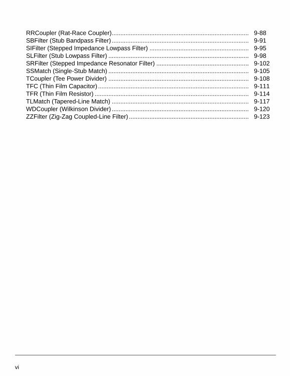
RRCoupler (Rat-Race Coupler)................................................................................ 9-88SBFilter (Stub Bandpass Filter) ................................................................................ 9-91SIFilter (Stepped Impedance Lowpass Filter) .......................................................... 9-95SLFilter (Stub Lowpass Filter) .................................................................................. 9-98SRFilter (Stepped Impedance Resonator Filter) ...................................................... 9-102SSMatch (Single-Stub Match) .................................................................................. 9-105TCoupler (Tee Power Divider) .................................................................................. 9-108TFC (Thin Film Capacitor) ........................................................................................ 9-111TFR (Thin Film Resistor) .......................................................................................... 9-114TLMatch (Tapered-Line Match) ................................................................................ 9-117WDCoupler (Wilkinson Divider) ................................................................................ 9-120ZZFilter (Zig-Zag Coupled-Line Filter) ...................................................................... 9-123
vi
Chapter 1: Passive Circuit QuickStart GuideThe Passive Circuit QuickStart Guide is designed to have you effectively using thePassive Circuit DesignGuide very quickly. The DesignGuide allows you to design,simulate and optimize passive circuit components. This guide assumes you haveinstalled the DesignGuide with appropriate licensing codewords.
For further details on the Design Guide features, refer to chapters 2 through 9 of thismanual, which provides complete information on the DesignGuide.
Note This manual is written describing and showing access through the cascadingmenu preference. If you are running the program through the selection dialog boxmethod, the appearance and interface will be slightly different.
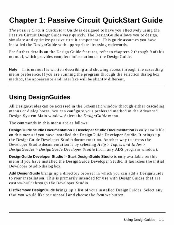
Using DesignGuidesAll DesignGuides can be accessed in the Schematic window through either cascadingmenus or dialog boxes. You can configure your preferred method in the AdvancedDesign System Main window. Select the DesignGuide menu.
The commands in this menu are as follows:
DesignGuide Studio Documentation > Developer Studio Documentation is only availableon this menu if you have installed the DesignGuide Developer Studio. It brings upthe DesignGuide Developer Studio documentation. Another way to access theDeveloper Studio documentation is by selecting Help > Topics and Index >DesignGuides > DesignGuide Developer Studio (from any ADS program window).
DesignGuide Developer Studio > Start DesignGuide Studio is only available on thismenu if you have installed the DesignGuide Developer Studio. It launches the initialDeveloper Studio dialog box.
Add DesignGuide brings up a directory browser in which you can add a DesignGuideto your installation. This is primarily intended for use with DesignGuides that arecustom-built through the Developer Studio.
List/Remove DesignGuide brings up a list of your installed DesignGuides. Select anythat you would like to uninstall and choose the Remove button.
Using DesignGuides 1-1
Passive Circuit QuickStart Guide
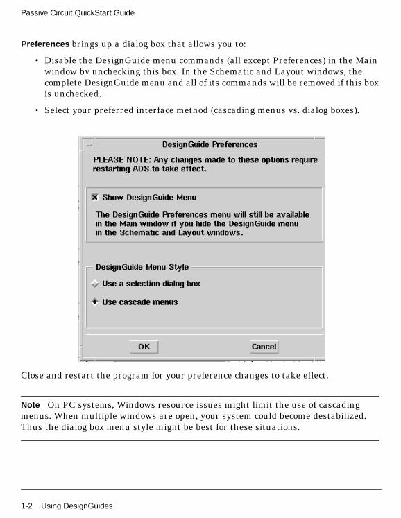
Preferences brings up a dialog box that allows you to:
• Disable the DesignGuide menu commands (all except Preferences) in the Mainwindow by unchecking this box. In the Schematic and Layout windows, thecomplete DesignGuide menu and all of its commands will be removed if this boxis unchecked.
• Select your preferred interface method (cascading menus vs. dialog boxes).
Close and restart the program for your preference changes to take effect.
Note On PC systems, Windows resource issues might limit the use of cascadingmenus. When multiple windows are open, your system could become destabilized.Thus the dialog box menu style might be best for these situations.
1-2 Using DesignGuides

Guide to Passive Circuit Documentation
The chapters of this manual include the following:
1. Chapter 1, Passive Circuit QuickStart Guide is the recommended starting pointfor users. Review this chapter for a quick overview of using this DesignGuide.
2. Chapter 2, How Do I? includes specific questions on DesignGuide usage. Itanswers many of the commonly asked questions about the DesignGuide.
3. Chapter 3, SmartComponents explains how to use SmartComponents.
4. Chapter 4, Design Assistant explains how to generate SmartComponentdesigns.
5. Chapter 5, Simulation Assistant explains how to analyze SmartComponentdesigns.
6. Chapter 6, Optimization Assistant explains how to optimize SmartComponentdesigns.
7. Chapter 7, Display Assistant explains how to display SmartComponentsimulation results.
8. Chapter 8, Layout Generation explains the steps required to generate a layout.
9. Chapter 9, SmartComponent Reference describes each SmartComponent indetail.
Using DesignGuides 1-3

Passive Circuit QuickStart Guide
Using the DesignGuideThe Passive Circuit DesignGuide provides SmartComponents andautomated-assistants for the design, simulation, optimization and performanceanalysis of common passive microstrip structures. SmartComponents are includedfor microstrip structures such as lines, couplers, power dividers, filters, and matchingnetworks. Automated-assistants include a Design Assistant, Simulation Assistant,Optimization Assistant and Display Assistant, which allow you to quickly create andverify a design. All SmartComponents can be modified when selected. You simplyselect a SmartComponent and with little effort redesign or verify its performance.
The complexity of Advanced Design System (ADS) is made easily accessible to thedesigner through the automated assistants. This allows a first-time or casual ADSuser to begin benefiting from the capability of ADS quickly. Experienced ADS userswill be able to perform tasks faster than ever before. As an example, a microstripcoupled-line filter can be designed, verified and a layout generated in a few minutessaving the designer substantial time.
1-4 Using the DesignGuide
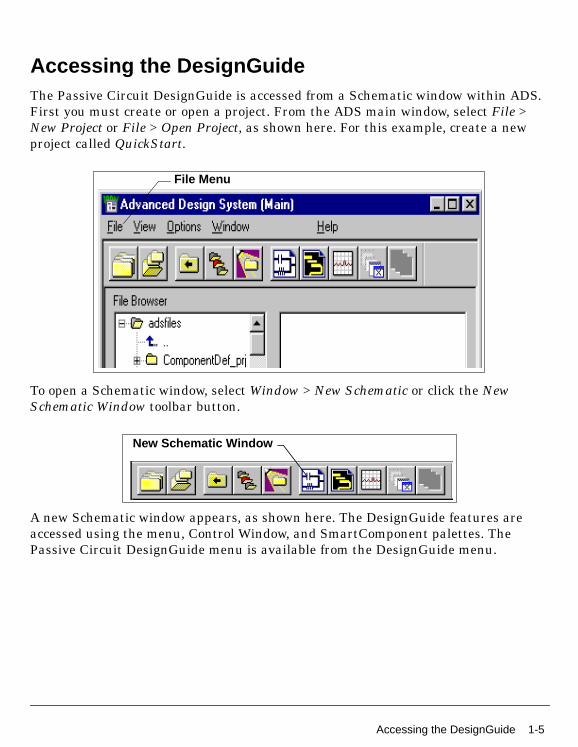
Accessing the DesignGuideThe Passive Circuit DesignGuide is accessed from a Schematic window within ADS.First you must create or open a project. From the ADS main window, select File >New Project or File > Open Project, as shown here. For this example, create a newproject called QuickStart.
To open a Schematic window, select Window > New Schematic or click the NewSchematic Window toolbar button.
A new Schematic window appears, as shown here. The DesignGuide features areaccessed using the menu, Control Window, and SmartComponent palettes. ThePassive Circuit DesignGuide menu is available from the DesignGuide menu.
File Menu
New Schematic Window
Accessing the DesignGuide 1-5
Passive Circuit QuickStart Guide
Note Depending on how your ADS preferences are set, a Schematic window mayautomatically appear when you create or open a project.
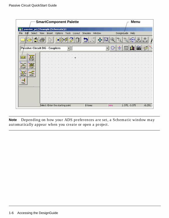
MenuSmartComponent Palette
1-6 Accessing the DesignGuide
Navigating Through the DesignGuideThe DesignGuide features are accessed by sselecting, from the Schematic window,DesignGuide> Passive Circuit.
Accessing the Documentation
To access the documentation for the DesignGuide, select either of the following:
• DesignGuide > Passive Circuit > Passive Circuit DesignGuide Documentation(from ADS Schematic window)
• Help > Topics and Index > DesignGuides > Passive Circuits (from any ADSprogram window)
Navigating Through the DesignGuide 1-7

Passive Circuit QuickStart Guide
Control Window Access
All features are available from the Control Window that includes menus, a toolbar,and SmartComponent manipulation controls. To access the Control Window, selectPassive Circuit Control Window from the Passive Circuit menu.
ToolbarMenus
Passive Circuit DesignGuide Control Window
Tab Pages
1-8 Navigating Through the DesignGuide
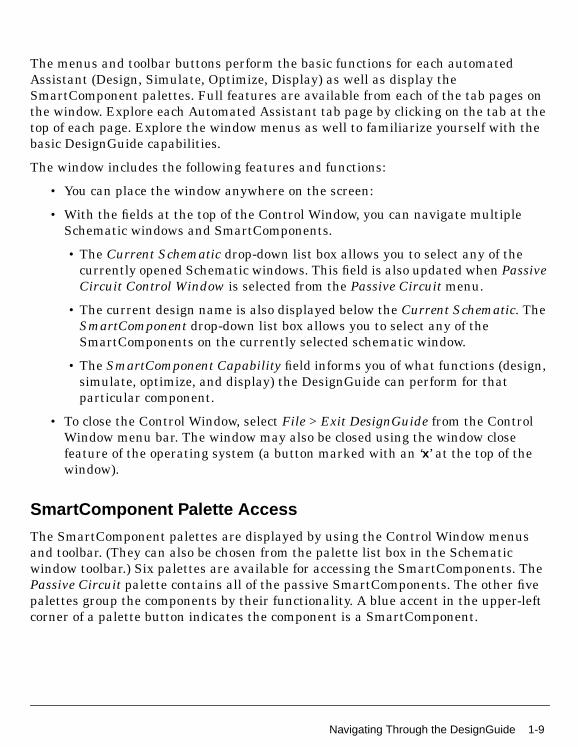
The menus and toolbar buttons perform the basic functions for each automatedAssistant (Design, Simulate, Optimize, Display) as well as display theSmartComponent palettes. Full features are available from each of the tab pages onthe window. Explore each Automated Assistant tab page by clicking on the tab at thetop of each page. Explore the window menus as well to familiarize yourself with thebasic DesignGuide capabilities.
The window includes the following features and functions:
• You can place the window anywhere on the screen:
• With the fields at the top of the Control Window, you can navigate multipleSchematic windows and SmartComponents.
• The Current Schematic drop-down list box allows you to select any of thecurrently opened Schematic windows. This field is also updated when PassiveCircuit Control Window is selected from the Passive Circuit menu.
• The current design name is also displayed below the Current Schematic. TheSmartComponent drop-down list box allows you to select any of theSmartComponents on the currently selected schematic window.
• The SmartComponent Capability field informs you of what functions (design,simulate, optimize, and display) the DesignGuide can perform for thatparticular component.
• To close the Control Window, select File > Exit DesignGuide from the ControlWindow menu bar. The window may also be closed using the window closefeature of the operating system (a button marked with an ‘x’ at the top of thewindow).
SmartComponent Palette Access
The SmartComponent palettes are displayed by using the Control Window menusand toolbar. (They can also be chosen from the palette list box in the Schematicwindow toolbar.) Six palettes are available for accessing the SmartComponents. ThePassive Circuit palette contains all of the passive SmartComponents. The other fivepalettes group the components by their functionality. A blue accent in the upper-leftcorner of a palette button indicates the component is a SmartComponent.
Navigating Through the DesignGuide 1-9
Passive Circuit QuickStart Guide
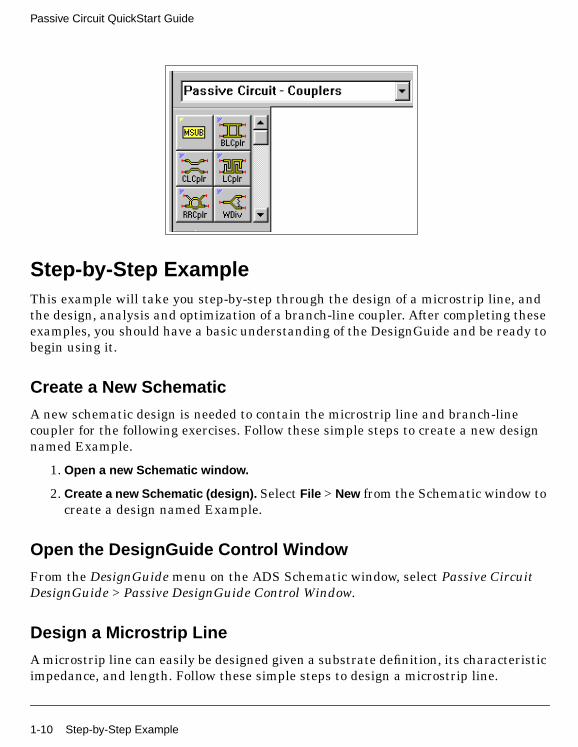
Step-by-Step ExampleThis example will take you step-by-step through the design of a microstrip line, andthe design, analysis and optimization of a branch-line coupler. After completing theseexamples, you should have a basic understanding of the DesignGuide and be ready tobegin using it.
Create a New Schematic
A new schematic design is needed to contain the microstrip line and branch-linecoupler for the following exercises. Follow these simple steps to create a new designnamed Example.
1. Open a new Schematic window.
2. Create a new Schematic (design). Select File > New from the Schematic window tocreate a design named Example.
Open the DesignGuide Control Window
From the DesignGuide menu on the ADS Schematic window, select Passive CircuitDesignGuide > Passive DesignGuide Control Window.
Design a Microstrip Line
A microstrip line can easily be designed given a substrate definition, its characteristicimpedance, and length. Follow these simple steps to design a microstrip line.
1-10 Step-by-Step Example
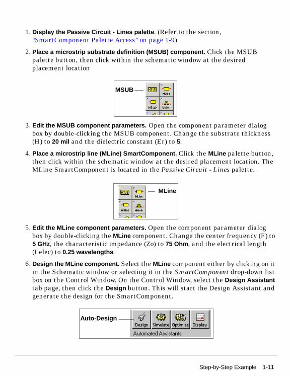
1. Display the Passive Circuit - Lines palette. (Refer to the section,“SmartComponent Palette Access” on page 1-9)
2. Place a microstrip substrate definition (MSUB) component. Click the MSUBpalette button, then click within the schematic window at the desiredplacement location
3. Edit the MSUB component parameters. Open the component parameter dialogbox by double-clicking the MSUB component. Change the substrate thickness(H) to 20 mil and the dielectric constant (Er) to 5.
4. Place a microstrip line (MLine) SmartComponent. Click the MLine palette button,then click within the schematic window at the desired placement location. TheMLine SmartComponent is located in the Passive Circuit - Lines palette.
5. Edit the MLine component parameters. Open the component parameter dialogbox by double-clicking the MLine component. Change the center frequency (F) to5 GHz, the characteristic impedance (Zo) to 75 Ohm, and the electrical length(Lelec) to 0.25 wavelengths.
6. Design the MLine component. Select the MLine component either by clicking on itin the Schematic window or selecting it in the SmartComponent drop-down listbox on the Control Window. On the Control Window, select the Design Assistanttab page, then click the Design button. This will start the Design Assistant andgenerate the design for the SmartComponent.
MSUB
MLine
Auto-Design
Step-by-Step Example 1-11

Passive Circuit QuickStart Guide
7. Examine the MLine design. Select the component MLine and click the Push IntoHierarchy toolbar button. After examining the design, pop out of theSmartComponent by clicking the Pop Out of Hierarchy toolbar button.
8. Delete the MLine SmartComponent. Select Tools > Delete SmartComponent fromthe DesignGuide Control Window menu.
Note This is different from the Delete button on the ADS Schematic windowtoolbar.
Design and Analyze a Branch-Line Coupler
A branch-line coupler can be designed as easily as a microstrip line. Follow thesesimple steps to design and analyze a branch-line coupler.
1. Place a branch-line coupler (BLCoupler) SmartComponent. Click the BLCplrpalette button and then click within the schematic window at the desiredplacement location. The BLCoupler SmartComponent is in the Passive Circuit -Couplers palette.
2. Edit the branch-line coupler parameters. Change the center frequency (F) to 5GHz.
3. Design the branch-line coupler. Select the BLCoupler component in theSmartComponent drop-down list box on the Control Window and then click theDesign button on the Design Assistant tab page. This will start the DesignAssistant and generate the design for the SmartComponent.
4. Analyze (simulate) the branch-line coupler. Select the Simulation Assistant tabpage on the Control Window and click the Simulate button (accept default
Push Into Hierarchy
Auto-Generated Design for MLine
Pop Out of Hierarchy
1-12 Step-by-Step Example

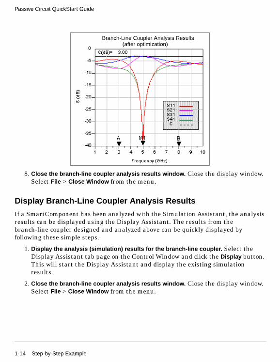
frequency/display specifications). This will invoke the Simulation Assistant andanalyze the SmartComponent. The analysis results are shown here.
5. Close the branch-line coupler analysis results window. Close the display windowby choosing File > Close Window from the menu.
Optimize the Branch-Line Coupler
The branch-line coupler as designed in the preceding section has a center frequencyof 5.5 GHz, which is different from the desired 5 GHz. The difference is due tolimitations of the synthesis method used to generate the design. However, theOptimization Assistant can be used to easily optimize the design so that the centerfrequency is as specified.
6. Optimize the branch-line coupler. Select the Optimization Assistant tab page onthe Control Window and click the Optimize button. This will start theOptimization Assistant and optimize the SmartComponent.
7. Re-analyze the branch-line coupler. Select the Simulation Assistant tab page onthe Control Window and click the Simulate button (accept defaultfrequency/display specifications). This will invoke the Simulation Assistant andre-analyze the branch-line coupler. The new analysis results are shown here.
Branch-Line Coupler Analysis Results
Step-by-Step Example 1-13
Passive Circuit QuickStart Guide
8. Close the branch-line coupler analysis results window. Close the display window.Select File > Close Window from the menu.
Display Branch-Line Coupler Analysis Results
If a SmartComponent has been analyzed with the Simulation Assistant, the analysisresults can be displayed using the Display Assistant. The results from thebranch-line coupler designed and analyzed above can be quickly displayed byfollowing these simple steps.
1. Display the analysis (simulation) results for the branch-line coupler. Select theDisplay Assistant tab page on the Control Window and click the Display button.This will start the Display Assistant and display the existing simulationresults.
2. Close the branch-line coupler analysis results window. Close the display window.Select File > Close Window from the menu.
Branch-Line Coupler Analysis Results(after optimization)
1-14 Step-by-Step Example

General ConceptsThere are two important general concepts: SmartComponents and AutomatedAssistants. The DesignGuide provides a large number of passive SmartComponentssuch as couplers, filters, and matching networks. SmartComponents containspecification parameters and a schematic representation of the design.Smart-Components are manipulated using several Automated Assistants. Theseassistants allow you to easily design, simulate, and optimize the SmartComponents.
Design Flow
The use of the DesignGuide follows a normal design procedure:
1. Select a component needed for your design.
2. Provide specifications.
3. Design and analyze the component.
4. If the component performance needs adjustment, optimize the component.
SmartComponent Setup
1. Choose and place a SmartComponent.
2. Edit the SmartComponent parameters (specifications).
SmartComponent Design and Analysis
3. Design the SmartComponent using the DesignAssistant.
4. Analyze the SmartComponent’s performance using the SimulationAssistant.
5. Display the performance of the SmartComponent using the DisplayAssistant.
Optional SmartComponent Optimization
6. If necessary, optimize the SmartComponent’s performance using theOptimization Assistant.
7. Re-analyze the SmartComponent’s performance using the SimulationAssistant.
General Concepts 1-15
Passive Circuit QuickStart Guide
Use of SmartComponents
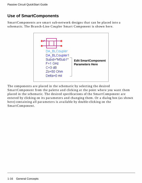
SmartComponents are smart sub-network designs that can be placed into aschematic. The Branch-Line Coupler Smart Component is shown here.
The components are placed in the schematic by selecting the desiredSmartComponent from the palette and clicking at the point where you want themplaced in the schematic. The desired specifications of the SmartComponent areentered by clicking on its parameters and changing them. Or a dialog box (as shownhere) containing all parameters is available by double-clicking on theSmartComponent.
Edit SmartComponentParameters Here
1-16 General Concepts

The SmartComponent design (schematic) can be viewed by pushing into theSmartComponent’s subnetwork. A SmartComponent subnetwork is empty until theDesign Assistant is used to generate the design. For details on theSmartComponents, refer to Chapter 9, SmartComponent Reference.
Hint Place a branch-line coupler SmartComponent into a schematic by clicking theBLCplr palette button and clicking within the Schematic window at the desiredplacement location. Open the parameter dialog box by double-clicking the branch-linecoupler component and edit its parameters.
Edit SmartComponentParameters Here
General Concepts 1-17
Passive Circuit QuickStart Guide
Automated-Assistants
Four Automated Assistants are available in this DesignGuide. They provide quickdesign, simulation, optimization and analysis display of SmartComponents. EachAutomated Assistant has a tab that is accessed from DesignGuide Control Window.Explore each tab on the Control Window. Following are descriptions of eachAutomated Assistant.
Design Assistant is used to generate/update a SmartComponent’s schematicdesign. After a SmartComponent is placed and the parameters are specified,you start the Design Assistant to design the component. Subsequently, if the
parameters of the SmartComponent are modified, you start the Design Assistantagain to update the design. For more information, refer to Chapter 4, DesignAssistant.
Simulation Assistant is used to automatically perform a simulation of aSmartComponent. After a SmartComponent has been designed using theDesign Assistant, you start the Simulation Assistant to automatically
analyze the component. You can easily examine the simulation results using theDisplay Assistant. For more information, refer to Chapter 5, Simulation Assistant.
Optimization Assistant is used to automatically optimize a SmartComponentdesign so that the desired specifications are achieved. After aSmartComponent has been analyzed using the Simulation Assistant, you
can start the Optimization Assistant to automatically optimize the component. Afterthe Optimization Assistant has finished, you can rerun the Simulation Assistant toexamine the optimized performance of the SmartComponent. For more information,refer to Chapter 6, Optimization Assistant.
Display Assistant is used to automatically display the analysis resultsgenerated using the Simulation Assistant. By starting the DisplayAssistant, you can quickly display the results generated from the most
recent simulation of a SmartComponent. For more detailed see Chapter 7, DisplayAssistant.
1-18 General Concepts

Chapter 2: How Do I?This chapter provides answers to many common questions about the Passive CircuitDesignGuide. Select a topic from the list below to see a more detailed list ofquestions. The questions are provided to help you quickly find the answer you need.
How Do I TopicsHow Do I Use SmartComponents?
How Do I Design (Synthesize) SmartComponents?
How Do I Simulate (Analyze) SmartComponents?
How Do I Optimize SmartComponents?
How Do I Display Simulation (Analysis) Results?
How Do I Layout SmartComponent Artwork?
How Do I Topics 2-1
How Do I?
How Do I Use SmartComponents?
Place
How do I place a new SmartComponent into a design?
How do I place an existing SmartComponent from the current project into a design?
How do I place an existing SmartComponent from a different project into a design?
Copy/Edit
How do I copy a SmartComponent within a design?
How do I copy a SmartComponent from one design to another?
How do I copy a SmartComponent from one Schematic Window to another?
How do I copy a SmartComponent and make it a new SmartComponent, not just anew instance?
How do I edit a SmartComponent?
Delete
How do I delete a SmartComponent from a design?
How do I completely delete a SmartComponent’s files from a project?
Stand Alone Usage
How do I use a SmartComponent without the DesignGuide?
How do I use a SmartComponent within the same project?
How do I use a SmartComponent from another project?
Specific SmartComponent Properties
How do I get information on the properties of a specific SmartComponent?
2-2 How Do I Use SmartComponents?
SmartComponent Manipulation Answers
How do I place a new SmartComponent into a design?
SmartComponents are placed into a design using the DesignGuide palettes. Refer tothe section Placing SmartComponents in the chapter SmartComponents for completeinstructions.
How do I place an existing SmartComponent from the current projectinto a design?
Any existing SmartComponent in the current project can be placed into a designusing the Component Library. Refer to the section Using an ExistingSmartComponent Within the Same Project in the chapter SmartComponents forcomplete instructions.
How do I place an existing SmartComponent from a different project intoa design?
Any existing SmartComponent from another project can be placed into a design byincluding the project and using the Component Library to place it. Refer to thesection Using an Existing SmartComponent in Any Project in the chapterSmartComponents for complete instructions.
How do I copy a SmartComponent within a design?
To copy a SmartComponent within a design, refer to the section Copying Within ADesign in the chapter SmartComponents for complete instructions.
How do I copy a SmartComponent from one design to another?
To copy a SmartComponent from one design to another, refer to the section CopyingBetween Designs or Schematic Windows in the chapter SmartComponents forcomplete instructions.
How do I copy a SmartComponent from one Schematic Window toanother?
To copy a SmartComponent from one Schematic Window to another, refer to thesection Copying Between Designs or Schematic Windows in the chapterSmartComponents for complete instructions.
SmartComponent Manipulation Answers 2-3

How Do I?
How do I copy a SmartComponent and make it a new SmartComponent,not just a new instance?
All copied SmartComponents will initially refer to the same SmartComponentdesign. When the Design Assistant is used to perform a design or update operation, itwill transform each copied SmartComponent into a unique SmartComponent design.A design operation is accomplished by launching the Design Assistant.
How do I edit a SmartComponent?
A SmartComponent’s position, orientation, and parameters can be edited like anyother component in ADS. Refer to the section Editing SmartComponents in thechapter SmartComponents for complete instructions.
How do I delete a SmartComponent from a design?
A SmartComponent can be deleted from the current design just like any othercomponent in ADS. Refer to the section Delete From Current Design in the chapterSmartComponents for complete instructions.
How do I completely delete a SmartComponent’s files from a project?
A SmartComponent and its associated files can be completely removed from a projectby using the DesignGuide Delete SmartComponent command/or by using thecomputer’s file system. Refer to the section Delete From Current Project in thechapter SmartComponents for complete instructions.
How do I use a SmartComponent without the DesignGuide?
Once SmartComponents are designed and tested, they can be used as stand-alonecomponents. The Passive Circuit DesignGuide is not needed to use them in newdesigns unless you wish to modify or analyze them. Refer to the section Stand AloneSmartComponent Usage in the chapter SmartComponents for complete instructions.
How do I use a SmartComponent within the same project?
An existing SmartComponent present in the current project can be used in anydesign. Refer to the section Using an Existing SmartComponent Within the SameProject in the chapter SmartComponents for complete instructions.
2-4 SmartComponent Manipulation Answers

How do I use a SmartComponent from another project?
An existing SmartComponent from another project can be used in any design byincluding the project and using the Component Library to place it. Refer to thesection Using an Existing SmartComponent in Any Project in the chapterSmartComponents for complete instructions.
How do I get information on the properties of a specificSmartComponent?
Refer to Chapter 9, SmartComponent Reference for a description of each component.The properties and other information specific to a SmartComponent are given.
SmartComponent Manipulation Answers 2-5
How Do I?
How Do I Design (Synthesize) SmartComponents?
Design
How do I get information on the synthesis of a specific SmartComponent?
How do I find out about the Design Assistant?
How do I examine a synthesized design?
How do I force the redesign of a SmartComponent?
How do I force the redesign of all SmartComponents in a design?
Specific SmartComponent Design
How do I get information on the synthesis of a specific SmartComponent?
How do I find which SmartComponents can be synthesized with the DesignAssistant?
2-6 How Do I Design (Synthesize) SmartComponents?

SmartComponent Design Answers
How do I find out about the Design Assistant?
Refer to Chapter 4, Design Assistant for complete information on using the DesignAssistant.
How do I design (synthesize) a SmartComponent?
The Design Assistant is used to automatically synthesize a SmartComponent design.To accomplish this, you simply select the SmartComponent on the Control Windowand launch the Design Assistant. This will automatically design theSmartComponent. Refer to Chapter 4, Design Assistant for complete information.
How do I examine a synthesized design?
The design for a SmartComponent is contained within a sub-network design file. Thedesign is easily examined by selecting the Push Into Hierarchy toolbar button orchoosing View > Push Into Hierarchy from the Schematic window. When you arefinished examining the design, choose the Pop Out Of Hierarchy toolbar button orselect View > Pop Out Of Hierarchy from the Schematic Window.
How do I force the redesign of a SmartComponent?
The SmartComponent will be re-designed by selecting the SmartComponent on theControl Window and launching the Design Assistant.Refer to the section DesignAssistant Operation of the chapter Design Assistant for complete information.
How do I force the redesign of all SmartComponents in a design?
Choosing the Design All button from the DesignGuide Control Window will force theredesign of all SmartComponents in the current design. Refer to the section ControlWindow: Single Component Design in the chapter Design Assistant for completeinformation.
How do I get information on the synthesis of a specificSmartComponent?
Refer to Chapter 9, SmartComponent Reference for specific synthesis information oneach SmartComponent.
SmartComponent Design Answers 2-7
How Do I?
How do I find which SmartComponents can be synthesized with theDesign Assistant?
All SmartComponents included with the Passive Circuit DesignGuide can beautomatically synthesized using the Design Assistant.
How Do I Simulate (Analyze) SmartComponents?
Simulation (Analysis)
How do I find out about the Simulation Assistant?
How do I change the frequency sweep of a simulation?
How do I display the results of a simulation?
How do I examine the simulation circuit?
How do I perform a simulation manually?
Specific SmartComponent Simulation
How do I get information on the simulation of a specific SmartComponent?
How do I find which SmartComponents can be analyzed with the SimulationAssistant?
SmartComponent Simulation Answers
How do I find out about the Simulation Assistant?
Refer to Chapter 5, Simulation Assistant for complete information on using theSimulation Assistant.
How do I simulate (analyze) a SmartComponent?
The Simulation Assistant is used to automatically simulate a SmartComponentdesign. To accomplish this, you simply select the SmartComponent on the ControlWindow and launch the Simulation Assistant. This will automatically simulate theSmartComponent. Refer to Chapter 5, Simulation Assistant for completeinformation.
2-8 How Do I Simulate (Analyze) SmartComponents?

How do I change the frequency sweep of a simulation?
The frequency sweep for a simulation is set by specifying the start, stop, and step sizefound on the Simulation Assistant tab page on the Control Window. Refer to thesection Simulation Frequency Sweep in the chapter Simulation Assistant forcomplete instructions.
How do I display the results of a simulation?
To have the results of a simulation automatically displayed when a simulation ends,enable the automatic display option. Refer to the section Automatically DisplayResults in Chapter 5, Simulation Assistant for complete instructions on enabling theautomatic display option. The Display Assistant can also be used to display theresults of a simulation. Refer to Chapter 7, Display Assistant for completeinstructions on displaying simulation results.
How do I examine the simulation circuit?
With the SmartComponent selected in the DesignGuide Control Window, pressCreate Template from the Simulation Assistant tab page. This will open thesimulation circuit used to analyze the SmartComponent. When you are finishedexamining the circuit, press the Update from Template button on the SimulationAssistant tab page. Refer to the section Simulation Templates in the chapterSimulation Assistant for more information.
How do I perform a simulation manually?
With the SmartComponent selected in the DesignGuide Control Window, pressCreate Template from the Simulation Assistant tab page. This will open thesimulation circuit used to analyze the SmartComponent. When you are finishedexamining the circuit, press the Update from Template button on the SimulationAssistant tab page. Refer to the section Simulation Templates in the chapterSimulation Assistant for more information.
How do I get information on the simulation of a specificSmartComponent?
Refer to Chapter 9, SmartComponent Reference for specific simulation informationon each SmartComponent.
SmartComponent Simulation Answers 2-9

How Do I?
How do I find which SmartComponents can be analyzed with theSimulation Assistant?
Most SmartComponents can be analyzed with the Simulation Assistant. Alldistributed RLC components, couplers, power dividers, filters, and matching circuitcomponents can be simulated with the Simulation Assistant. The SmartComponentson the Lines menu and palette can not be simulated with the Simulation Assistantbecause of their simplicity. The SmartComponent Capability field on the DesignGuideControl Window indicates if the currently selected component can be analyzed.
How Do I Optimize SmartComponents?
Optimization
How do I find out about the Optimization Assistant?
How do I update a design with parameters from an optimization?
How do I examine the optimization circuit?
How do I perform an optimization manually?
How do I change the goals of an optimization?
How do I proceed when an optimization is not successful?
Specific SmartComponent Optimization
How do I get information on optimization related to a specific SmartComponent?
How do I find which SmartComponents can be optimized with the OptimizationAssistant?
SmartComponent Optimization Answers
How do I find out about the Optimization Assistant?
Refer to Chapter 6, Optimization Assistant for complete information on using theOptimization Assistant.
2-10 How Do I Optimize SmartComponents?
How do I optimize a SmartComponent?
The Optimization Assistant is used to automatically optimize a SmartComponentdesign. To accomplish this, you simply select the SmartComponent on the ControlWindow and launch the Optimization Assistant. This will automatically optimize theSmartComponent. Refer to Chapter 6, Optimization Assistant for completeinformation.
How do I update a design with parameters from an optimization?
The Optimization Assistant will update the SmartComponent automatically. If theoptimization has been performed manually using the optimization template, use theUpdate from Template button from the Optimization Assistant tab page on theControl Window to update the SmartComponent. Refer to the section OptimizationTemplates in the chapter Optimization Assistant for more information.
How do I examine the optimization circuit?
With the SmartComponent selected in the DesignGuide Control Window, pressCreate Template from the Optimization Assistant tab page. This will open the circuitused to optimize the SmartComponent. When you are finished examining the circuit,press the Update from Template button on the Simulation Assistant tab page. Referto the section Optimization Templates in the chapter Optimization Assistant formore information.
How do I perform an optimization manually?
With the SmartComponent selected in the DesignGuide Control Window, pressCreate Template from the Optimization Assistant tab page. This will open the circuitused to optimize the SmartComponent. When you are finished examining the circuit,press the Update from Template button on the Simulation Assistant tab page. Referto the section Optimization Templates in the chapter Optimization Assistant formore information.
How do I change the goals of an optimization?
With the SmartComponent selected in the DesignGuide Control Window, pressCreate Template from the Optimization Assistant tab page. This will open theoptimization circuit. Edit the optimization goals. Refer to Chapter 9,SmartComponent Reference for specific optimization information on eachSmartComponent. Optimize the circuit by selecting Simulate > Simulate from the
SmartComponent Optimization Answers 2-11

How Do I?
Schematic Window. When you are finished examining the circuit, press the Updatefrom Template button on the Simulation Assistant tab page. Refer to the sectionOptimization Templates in the chapter Optimization Assistant for more information.
How do I proceed when an optimization is not successful?
If the optimization fails, the optimization goals can usually be adjusted to fix theproblem. Refer to Chapter 9, SmartComponent Reference for specific optimizationinformation on each SmartComponent.
How do I get information on optimization related to a specificSmartComponent?
Refer to Chapter 9, SmartComponent Reference for specific optimization informationon each SmartComponent.
How do I find which SmartComponents can be optimized with theOptimization Assistant?
Most SmartComponents can be optimized with the Optimization Assistant. Allcouplers, power dividers, and filters and most of the matching circuits anddistributed RLC components can be optimized with the Optimization Assistant. TheSmartComponents on the Lines menu and palette and the rectangular spiralinductors can not be optimized with the Optimization Assistant. TheSmartComponent Capability field on the DesignGuide Control Window indicates ifthe currently selected component can be optimized.
How Do I Display Simulation (Analysis) Results?
Display Results
How do I get information on a specific SmartComponent’s display template?
How do I display the results from a SmartComponent simulation?
How do I open a specific display template manually?
How do I learn about the different components and features of the SmartComponentdisplay templates?
2-12 How Do I Display Simulation (Analysis) Results?

Specific SmartComponent Display Template
How do I get information on a specific SmartComponent’s display template?
Simulation Display Answers
How do I find out about the Display Assistant?
Refer to Chapter 7, Display Assistant for complete information on using the DisplayAssistant.
How do I display the results from a SmartComponent simulation?
The Display Assistant is used to automatically display the results of aSmartComponent simulation. To accomplish this, you simply select theSmartComponent on the Control Window and launch the Display Assistant. This willautomatically display the simulation results for the SmartComponent. Refer toChapter 7, Display Assistant for complete information.
How do I open a specific display template manually?
From the Display Assistant tab page on the Control Window, select the desireddisplay from the Available Templates field and press the Open Display Templatebutton. This will open the selected display. Refer to the section Display Templates inthe chapter Display Assistant for complete information.
How do I learn about the different components and features of theSmartComponent display templates?
Refer to the section Display Template Features in the chapter Display Assistant forinformation on the different components and features of the display templates.
How do I get information on a specific SmartComponent’s displaytemplate?
Refer to Chapter 9, SmartComponent Reference for display template information oneach SmartComponent.
Simulation Display Answers 2-13
How Do I?
How Do I Layout SmartComponent Artwork?
Create Layout
How do I automatically create artwork for SmartComponents?
Update Layout
How do I update artwork when I make changes or redesign a SmartComponent?
Layout of Specific SmartComponents
How do I get information on the layout of specific SmartComponents?
SmartComponent Artwork Layout Answers
How do I automatically create artwork for SmartComponents?
Artwork for all of the passive circuit SmartComponents in this DesignGuide can beautomatically generated. The Generate Layout capability of ADS is used to generatethe artwork for the SmartComponents. Refer to the section Layout Artwork Creationin the chapter Layout Generation for complete information.
How do I update artwork when I make changes or redesign aSmartComponent?
Refer to the section Layout Artwork Update in the chapter Layout Generation forcomplete information.
How do I get information on the layout of specific SmartComponents?
Refer to Chapter 9, SmartComponent Reference for layout information on eachSmartComponent.
2-14 How Do I Layout SmartComponent Artwork?

Chapter 3: SmartComponentsThis DesignGuide provides a large number of passive SmartComponents such ascouplers, filters, lines and matching networks. SmartComponents are smartsub-network designs that can be placed into a schematic and provide the containerfor specification parameters and a schematic representation of the design. Severalautomated-assistants allow you to easily design, simulate (analyze) and optimize theSmartComponents.
SmartComponent BasicsSmartComponents can be placed, copied, edited and deleted like other components inthe Advanced Design System. The basics of placement, copying, editing and deletingare described here.
Placing SmartComponents
The DesignGuide contains six SmartComponent palettes that provide quick and easyaccess to the SmartComponents. To place a SmartComponent:
1. Click on the desired component button in a SmartComponent palette.
2. Click within the Schematic window at the location you want theSmartComponent placed.
3. You may change the orientation of the SmartComponent before placement byselecting from the Insert > Component > Component Orientation commands or byrepeatedly selecting Rotate by -90 from the schematic toolbar.
4. The place component mode will remain active until you choose End Commandfrom the Schematic toolbar.
The six available component palettes are:
• All contains all of the SmartComponents.
• Lines contains the simple line element SmartComponents.
• RLC contains the distributed resistor, inductor, and capacitorSmartComponents.
• Couplers contains the coupler and power divider SmartComponents.
• Filters contains the distributed filter SmartComponents.
SmartComponent Basics 3-1
SmartComponents
• Match contains the distributed and lumped matching SmartComponents.
There are two methods to display the desired SmartComponent palette.
• Open the Passive Circuit DesignGuide Control Window by selectingDesignGuide > Passive Circuit DesignGuide > Passive DesignGuide ControlWindow. Display the desired SmartComponent palette by selecting one of theComponent Palette buttons from the control window toolbar or by selecting View> Component Palette - <Palette Name> from the control window menu.
• Select the desired SmartComponent palette from the Component Palettedrop-down list box in the Schematic window toolbar (directly above the palette).
Note When a SmartComponent is initially placed, a temporary component is used toinitially place and specify the parameters for the SmartComponent. This componentdoes not contain a subnetwork design. After the Design Assistant has been used todesign the SmartComponent, the temporary component is replaced with a permanentcomponent. The SmartComponent is renamed to DA_ComponentName_DesignNameand an autogenerated design is placed inside the SmartComponent’s subnetworkdesign file. Subsequently, if the SmartComponent parameters are edited, the DesignAssistant will need to be used again to update the subnetwork design file.
Copying SmartComponents
SmartComponents can be copied within a design, to another design, or to anotherSchematic window.
Copying Within A Design
1. Click the SmartComponent to be copied.
2. Select Edit > Copy, then Edit > Paste from the schematic window.
3. Click the spot where you want the copy placed.
Copying Between Designs or Schematic Windows
1. Click the SmartComponent to be copied.
2. Select Edit > Copy from the Schematic window.
3-2 SmartComponent Basics

3. Display the design or Schematic window you want to copy the SmartComponentto.
4. Select Edit > Paste to copy the SmartComponent to the design.
5. Click where you want the component placed.
Note All copied SmartComponents will initially refer to the same SmartComponentdesign. When the Design Assistant is used to perform a design operation, it willtransform each copied SmartComponent into a unique SmartComponent design. Adesign operation is accomplished by launching the Design Assistant from theDesignGuide Control Window.
Editing SmartComponents
A SmartComponent’s position, orientation, and parameters can be edited like anyother component in ADS.
Position and Orientation
A SmartComponent is moved by dragging it to any location in the Schematic window.It’s orientation is changed by following these steps.
1. Select Edit > Advanced Rotate/Mirror > Rotate from the Schematic window orselect Rotate Items from the toolbar.
2. Click on the desired SmartComponent.
3. Rotate the component.
4. The rotate mode will remain active until you select the End Command from thetoolbar.
Parameters
Parameters are changed by clicking on a SmartComponent parameter in theSchematic window and editing it or by double-clicking a component and editing theparameters in the component dialog box.
SmartComponent Basics 3-3
SmartComponents
Deleting SmartComponents
SmartComponents can be deleted from a design like other components, butcompletely removing a SmartComponent’s files requires the actions described here.
Delete From Current Design
A SmartComponent can be deleted from a design by selecting the component andpressing the Delete key, selecting Delete from the toolbar, or by selecting Edit > Deletefrom the Schematic window. However, this does not remove the SmartComponentfiles from the project directory.
Delete From Current Project
To delete a SmartComponent and all associated files from your project, follow thesesteps.
1. From the DesignGuide Control Window, select the Delete SmartComponentbutton.
2. Click on the SmartComponent you want deleted. This will delete theSmartComponent from the current design and remove all of its files from yourproject.
3. The SmartComponent delete mode will remain active until you select the EndCommand from the Schematic toolbar.
Delete Manually Using File System
You may use your computer’s file system to delete a SmartComponent by deleting theappropriate files in the network subdirectory of a project. Delete files that start withDA_, SA_’ and OA_, contain the SmartComponent title, and end with .ael or .dsn.
Design, Analysis, Optimization and LayoutThe DesignGuide contains several automated assistants that provide automaticdesign, analysis, and optimization for the SmartComponents. The followingassistants are available.
• Design Assistant. The Design Assistant is used to generate and update thedesign contained within a SmartComponent. It invokes a synthesis engine thatgenerates a design from the given specification. It will design and update a
3-4 Design, Analysis, Optimization and Layout
single SmartComponent or all SmartComponents in a design. Refer to Chapter4, Design Assistant for more information.
• Simulation (Analysis) Assistant. The Simulation Assistant is used to analyze thedesign contained within a SmartComponent. It creates a simulation circuitcontaining the SmartComponent, then performs a simulation. It can alsoautomatically display the results of the simulation. Refer to Chapter 5,Simulation Assistant for more information.
• Optimization Assistant. The Optimization Assistant is used to optimize thedesign contained within a SmartComponent. It creates an optimization circuitcontaining the SmartComponent, performs an optimization, and updates theSmartComponent. Refer to Chapter 6, Optimization Assistant for moreinformation.
• Display Assistant. The Display Assistant is used to quickly display theperformance of a SmartComponent. Display templates have been created formost of the SmartComponents. The display templates are preconfiguredtemplates which provide a comprehensive look at the component’s performance.Refer to Chapter 7, Display Assistant for more information.
• Automatic Layout Generation. Artwork for all of the passive circuitSmartComponents in this DesignGuide can be automatically generated. Thesynthesis engine used by the Design Assistant creates a schematic for theSmartComponents that is auto-layout-generation ready. The Generate Layoutcapability of ADS is used to generate the artwork for the SmartComponents.Refer to Chapter 8, Layout Generation for more information.
Stand Alone SmartComponent UsageOnce SmartComponents are designed and tested, they can be used as stand-alonecomponents. The Passive Circuit DesignGuide is not needed to use them in newdesigns unless you wish to modify or analyze them.
Using an Existing SmartComponent Within the Same Project
1. Open the Component Library window by selecting Insert > Component >Component Library from the Schematic window or Display Component LibraryList from the toolbar.
Stand Alone SmartComponent Usage 3-5
SmartComponents
2. Select the project name under All > Sub-networks in the Libraries list at the leftof the Component Library window. Available components will be listed in theComponents list at the right of the Component Library window.
3. Select the desired SmartComponent in the Components list.
4. Place the desired SmartComponent into your design by clicking in theSchematic window at the location you wish it placed.
5. The insert mode will remain active until you select End Command from thetoolbar.
Using an Existing SmartComponent in Any Project
A library of predesigned reusable SmartComponents can be easily created. This isdone by placing the reusable SmartComponents in a project. This project can beincluded in any project and its SmartComponents will be accessed using theComponent Library. Follow these steps.
1. Select File > Include/Remove Projects from the main ADS window.
2. Select the project that contains the desired SmartComponent from the FileBrowser at the left of the Include & Remove window.
3. Choose the Include button to include the project in the hierarchy.
4. Chose the OK button.
5. Open the Component Library window by selecting Insert > Component >Component Library from the Schematic window or Display Component LibraryList from the toolbar.
6. Select the included project name under All > Sub-networks in the Libraries listat the left of the Component Library window.
7. Available components will be listed in the Components list at the right of theComponent Library window.
8. Select the desired SmartComponent in the Components list.
9. Place the desired SmartComponent into your design by clicking in theSchematic window at the location you wish it placed.
10. The insert mode will remain active until you select End Command from thetoolbar.
3-6 Stand Alone SmartComponent Usage

Chapter 4: Design AssistantThe Design Assistant is used to generate and update the design contained within aSmartComponent from the given specifications. It will design and update a singleSmartComponent or all SmartComponents in a design.
The Design Assistant is accessed using the Passive Circuit DesignGuide ControlWindow. From the control window, full design control is enabled from the DesignAssistant tab. Single component design operations can also be accomplished using theControl Window menu and toolbar.
Design Assistant OperationFollowing are details on the use of the Design Assistant.
Control Window: Single Component Design
To design a single SmartComponent using the control window, select the desiredSmartComponent either from the SmartComponent drop-down list box in the upperright corner of the control window or by clicking on the component in the Schematicwindow. The design is accomplished using one of the following methods.
• Push the Design button on the Design Assistant tab. The design progress isindicated on the tab page.
• Push the Design button on the Control Wiindow toolbar.
• Select Tools > Auto-Design from the Control Window menu.
Control Window: Multiple Component Design
Selecting the Design All button on the Design Assistant tab designs allSmartComponents on the current Schematic. To avoid screen flicker associated withthe design, the Schematic window will disappear during the process. Design progressis indicated on the tab page.
Design Assistant Operation 4-1

Design Assistant
4-2 Design Assistant Operation
Chapter 5: Simulation AssistantThe Simulation Assistant is used to analyze the design contained within aSmartComponent. It creates a simulation circuit around the SmartComponent, thenperforms a simulation. If desired it will automatically display the simulation results.
The Simulation Assistant is accessed using the Passive Circuit DesignGuide ControlWindow. From the control window, full simulation control is enabled from theSimulation Assistant tab. Basic simulation can also be accomplished using the ControlWindow menu and toolbar.
Simulation Assistant OperationFor all simulation operations, the selected SmartComponent is designed if necessary,a simulation schematic is created, the simulation is performed, and the results aredisplayed. The simulation frequency sweep must be specified on the SimulationAssistant tab in the Control window.
Simulation Frequency Sweep
The simulation frequency sweep is specified on the Passive Circuit DesignGuidecontrol window. If you are performing the simulation from the Control Window, selectthe Simulation Assistant tab and specify the sweep by entering the start frequency,stop frequency, and either frequency step size or number of points. The valuesentered are stored in the selected SmartComponent (as displayed in theSmartComponent drop-down list box) and will be recalled each time thisSmartComponent is selected.
Note If a SmartComponent has been selected from the SmartComponent drop-downlist box on the control window, default frequencies will be set for the component
Automatically Display Results
If the Automatically Display Results box on the Control Window’s SimulationAssistant tab is selected, the simulation results will be automatically displayed uponcompletion of the analysis.
Simulation Assistant Operation 5-1
Simulation Assistant
Control Window
To simulate a SmartComponent using the control window, select the desiredSmartComponent either from the SmartComponent drop-down list box in the upperright corner of the control window or by clicking on the component on the schematicwindow. The simulation frequency sweep display option must be specified on theSimulation Assistant tab as previously described. The simulation is then accomplishedusing one of the following methods:
• Push the Simulate button on the Simulation Assistant tab.
• Push the Simulate button on the Control Window toolbar.
• Select Tools > Auto-Simulate from the Control Window menu.
Simulation TemplatesIn some cases it might be useful to manually simulate the SmartComponent. Togenerate a simulation schematic around the selected SmartComponent, press theCreate Template button on the control window Simulation Assistant tab. You canexamine or modify the simulation schematic, then manually start the simulation byselecting Simulate > Simulate from the Schematic window. When you are finished,pressing the Update from Template button on the Simulation Assistant tab willtransfer any changes you have made to the SmartComponent on the Simulationschematic to the original SmartComponent and redesign if necessary. You can alsomanually close the simulation schematic using File > Close Design from theSchematic window menu, although this will result is loss of any changes you havemade to the SmartComponent.
5-2 Simulation Templates

Chapter 6: Optimization AssistantThe Optimization Assistant is used to optimize the design contained within aSmartComponent. It creates a optimization circuit containing the SmartComponent,then performs an optimization.
The Optimization Assistant is accessed using the Passive Circuit DesignGuideControl Window. From the Control Window, full optimization control is enabled fromthe Optimization Assistant tab. Basic optimization can also be accomplished using thecontrol window menu and toolbar.
Optimization Assistant OperationFor all optimization operations, the selected SmartComponent is designed ifnecessary, an optimization schematic is created, and the optimization is performed.The optimization results are transferred to the original SmartComponent, and thisaltered component is redesigned. For each component, the optimization alters one ormore of the physical design dimensions in order to make the component responsemore closely meet the specified performance.
Control Window
To optimize a SmartComponent using the Control Window, select the desiredSmartComponent either from the SmartComponent drop-down list box in the upperright corner of the control window or by clicking on the component on the schematicwindow. The optimization is then accomplished using one of the following methods.
• Push the Optimize button on the Optimization Assistant tab.
• Push the Optimize button on the control window toolbar.
• Select Tools > Auto-Optimize from the control window menu.
The Optimization Assistant tab contains fields that indicate the objective of theoptimization operation as well as the physical parameters to be altered during theprocess.
Optimization TemplatesIn some cases it may be useful to manually optimize the SmartComponent. Togenerate an optimization schematic around the selected SmartComponent, press the
Optimization Assistant Operation 6-1

Optimization Assistant
Create Template button on the control window Optimization Assistant tab. You canexamine or modify the optimization schematic, then manually start the optimizationby selecting Simulate > Simulate from the Schematic window. When you are finished,selecting Simulate > Update Optimization Values will cause the optimized values toappear in the VAR element in the schematic lower left corner for your inspection.Pressing the Update from Template button on the Optimization Assistant tab willtransfer the optimization results to the original SmartComponent and redesign. Youmay also manually close the optimization schematic using File > Close Design fromthe Schematic window menu, although this will cause optimization results to be lost.
6-2 Optimization Templates

Chapter 7: Display AssistantThe Display Assistant is used to easily and quickly display the performance of aSmartComponent. Display templates have been created for most of theSmartComponents. This includes all of the RLC, coupler, filter and matchingcomponents. The line components do not have auto-simulation, auto-optimization orauto-display capability because of their simplicity. The display templates arepreconfigured templates that provide a comprehensive look at the performance of thecomponent. You can create your own displays or modify the included displaytemplates using the built in features of Advanced Design System, but in mostsituations, the included display templates will provide all the information you need.
The Display Assistant is accessed using either the Passive Circuit DesignGuideControl Window. From the control window, full display control is enabled from theDisplay Assistant tab. Basic display selection can also be accomplished using theControl Window menu and toolbar.
Display Template FeaturesThe display templates opened by the Display Assistant have common features thatare discussed here. For features unique to the display templates of someSmartComponents, refer to Chapter 9, SmartComponent Reference.
Basic Layout
Following is the basic layout of the display templates. Area one of the displaytemplate contains a graph of the most important parameters of theSmartComponent. Area two contains several graphs that give a comprehensive lookat the component’s performance. Area three contains a table listing the basicspecifications and performance of the component.
1.
2.
3.
Display Template Features 7-1

Display Assistant
Typical Area One Graph
A typical graph from area one of a display template follows. The frequency range ofthe graph is determined by the Simulation Assistant. As you change the frequencyrange in the Simulation Assistant, this graph will update appropriately. The markersA and B are used to define the frequency range of the graphs in area two. This featureis used to zero in on the region of interest and obtain a comprehensive look at thecomponent’s performance. The marker M1 can be moved by dragging it with themouse. The performance at the frequency given by M1 will be shown in the table inarea three.
Typical Area Two Graphs
Typical graphs from area 2 of a display template are shown here. These graphsprovide a quick, comprehensive look at the component’s performance. Theirfrequency range is determined by the location of the “A” and “B” markers found in themain graph. Any markers such as M2 shown here can be moved by dragging themwith the mouse. Performance criteria at the marker frequency will be displayed inthe table in area three.
7-2 Display Template Features
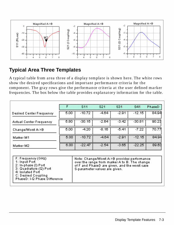
Typical Area Three Templates
A typical table from area three of a display template is shown here. The white rowsshow the desired specifications and important performance criteria for thecomponent. The gray rows give the performance criteria at the user defined markerfrequencies. The box below the table provides explanatory information for the table.
Display Template Features 7-3
Display Assistant
Display Assistant OperationBefore using the Display Assistant, a valid dataset from a simulation of the selectedSmartComponent must exist in the current project data directory. This simulationcan be conveniently accomplished using the Simulation Assistant. Refer to theSimulation Assistant chapter for details on this step.
Control Window
To display results from a SmartComponent simulation using the Control Window,select the desired SmartComponent either from the SmartComponent drop-down listbox in the upper right corner of the control window or by clicking on the componenton the schematic window. The display is then launched using one of the followingmethods.
• Push the Display button on the Display Assistant tab.
• Push the Display button on the control window toolbar.
• Select Tools > Auto-Display from the Control Window menu.
If no valid dataset exists for the selected SmartComponent, the Display button on theDisplay Assistant tab will be insensitive. If the toolbar or menu are used to try todisplay the results, a message will appear indicating that no dataset exists.
Display TemplatesIn some cases it may be useful to use one of the display templates provided with theDesignGuide for other applications. To gain access to one of these templates, selectthe desired template from the Available Templates field and press the OpenDisplayTemplate button on the control window Display Assistant tab. You can theninsert a dataset of your choice using the dataset pull-down list box in the upper leftcorner of the display. You may find that some parameters in the display template arenot defined in the selected dataset and may want to make appropriate modificationsto the display. These changes can be saved using the commands in the display Filemenu.
7-4 Display Assistant Operation

Chapter 8: Layout GenerationArtwork for all of the passive circuit SmartComponents in this DesignGuide can beautomatically generated. You need an Advanced Design System Layout license to usethis feature. The Design Assistant creates a schematic for the SmartComponentsthat is ready for auto-layout generation. The ADS Generate Layout capability is usedto generate the artwork for the SmartComponents.
Layout Artwork CreationTo create artwork for SmartComponents, follow these steps:
1. Choose and place the desired SmartComponents in the schematic window.
2. Specify the desired parameters for each SmartComponent.
3. Design the SmartComponents using the Design Assistant.
4. Select Layout > Generate/Update Layout from the Schematic window.
5. Choose OK in the Generate/Update Layout box.
The artwork for each SmartComponent and any other components that haveassociated artwork will be displayed in the Layout window. If the status reportcheckbox is selected in the Generate/Update Layout box, a layout generation statusreport will also be opened.
Layout Artwork UpdateTo edit the properties of a SmartComponent and update the associated artwork,follow these steps:
1. Choose the desired SmartComponent in the schematic window.
2. Edit the desired parameters of the SmartComponent.
3. Design the SmartComponent using the Design Assistant.
4. Select Layout > Generate/Update Layout from the Schematic window.
5. Select OK in the Generate/Update Layout box.
The artwork for the SmartComponent will be updated and displayed in the layoutwindow.
Layout Artwork Creation 8-1

Layout Generation
8-2 Layout Artwork Update
Chapter 9: SmartComponent Reference
SmartComponent List
Note A SmartComponent subnetwork is empty until the Design Assistant is used to generate thedesign. Refer to Chapter 4, Design Assistant.
Lines
MLine (Microstrip Line)
MStub (Microstrip Stub)
MMndr (Microstrip Meander Line)
MRStub (Microstrip Radial Stub)
MBStub (Microstrip Butterfly Radial Stub)
MCLine (Microstrip Coupled Line Component)
MBStub (Microstrip Butterfly Radial Stub)
MTaper (Microstrip Taper Component)
MStep (Microstrip Step Component)
MGap (Microstrip Gap Component)
MTee (Microstrip Tee Component)
MCross (Microstrip Cross Component)
MBend (Microstrip Bend Component)
MCorn (Microstrip Corner Component)
MCurve (Microstrip Curve Component)
Distributed Capacitors
MICapSG (Microstrip 1-port Interdigital Capacitor)
MICapS (Microstrip 2-port Interdigital Capacitor)
SmartComponent List 9-1
SmartComponent Reference
MICapPG (Microstrip Grounded 2-port Interdigital Capacitor)
MICapP (Microstrip 4-port Interdigital Capacitor)
MTFC (Microstrip Thin Film Capacitor)
TFC (Thin Film Capacitor)
Distributed Resistors
TFR (Thin Film Resistor)
Distributed Inductors
MRStub (Microstrip Radial Stub)
MRInd (Microstrip Rectangular Inductor)
MREInd (Microstrip Elevated Rectangular Inductor)
Couplers
BLCoupler (Branch-Line Coupler)
CLCoupler (Coupled-Line Coupler)
HPFilter (Hairpin Filter)
RRCoupler (Rat-Race Coupler)
Dividers
WDCoupler (Wilkinson Divider)
TCoupler (Tee Power Divider)
Filters
SIFilter (Stepped Impedance Lowpass Filter)
SLFilter (Stub Lowpass Filter)
CLFilter (Coupled-Line Filter)
ZZFilter (Zig-Zag Coupled-Line Filter)
SRFilter (Stepped Impedance Resonator Filter)
HPFilter (Hairpin Filter)
9-2 SmartComponent List
IDFilter (Interdigital Filter)
CMFilter (Comb-Line Filter)
SBFilter (Stub Bandpass Filter)
Matching Networks
LEMatch (Lumped Component Match)
SSMatch (Single-Stub Match)
CMFilter (Comb-Line Filter)
QWMatch (Quarter-Wave Match)
TLMatch (Tapered-Line Match)
SmartComponent List 9-3

SmartComponent Reference
BLCoupler (Branch-Line Coupler)
Symbol
Summary
A branch-line coupler outputs from the coupled port (pin 3) a fraction of the power presented atthe input (pin 1). The remainder of the power is passed through to the output port (pin 2). At thecenter frequency the phase difference between the outputs is 90 degrees, with the coupled portrepresenting the quadrature (Q) output and the output port representing the in-phase (I) output. Thecoupling coefficient specifies the ratio of the input power to the coupled power (P1/P3). Pin 4
represents the isolated port, and it is typically well isolated from the input port near the centerfrequency.
Note A SmartComponent subnetwork is empty until the Design Assistant is used to generate thedesign. Refer to Chapter 4, Design Assistant.
Parameters
Subst = microstrip substrate name
F = center frequency, in hertz
C = coupling coefficient, in dB
Zo = characteristic impedance, in ohms
Delta = length added to branches for tuning performance
Palette
Passive Circuit - Couplers
Available Automated-Assistants
Design Assistant, Simulation Assistant, Optimization Assistant, Display Assistant
Design Assistant Usage
For general information, refer to Chapter 4, Design Assistant.
9-4 SmartComponent List

1. The coupling coefficient must be positive and greater than 3 dB. Best results are obtainedfor tight couplings of 6 dB or better (C < 6 dB). Choosing the coupling parameter largerthan 6 dB often causes width constraint violations to occur on the MTEE components,resulting in warning messages during design and simulation. A coupling coefficient of 3 dBprovides an equal power split between the two outputs.
2. For a more detailed discussion of this device, see: D. M. Pozar, Microwave Engineering,2nd Edition, John Wiley & Sons: New York, 1998, pp. 379-383.
Simulation Assistant Usage
For general information, refer to Chapter 5, Simulation Assistant.
Optimization Assistant Usage
For general information, refer to Chapter 6, Optimization Assistant.
The optimization minimizes the input reflection coefficient (S11) at the design center frequency bychanging the length of the lines forming the four branches. All branches are changed by the samephysical length during the optimization.This optimization generally provides very good results butmay not guarantee that the specified coupling is attained at the design frequency. More advancedtuning can be performed by changing line width of the branch lines.
Display Assistant Usage
For general information, refer to Chapter 7, Display Assistant.
Example
A branch-line coupler was designed for a center frequency of 5 GHz with an equal power splitbetween the I and Q ports. Tuning using the Optimization Assistant yielded a value of Delta =49.532 mil.
SmartComponent List 9-5
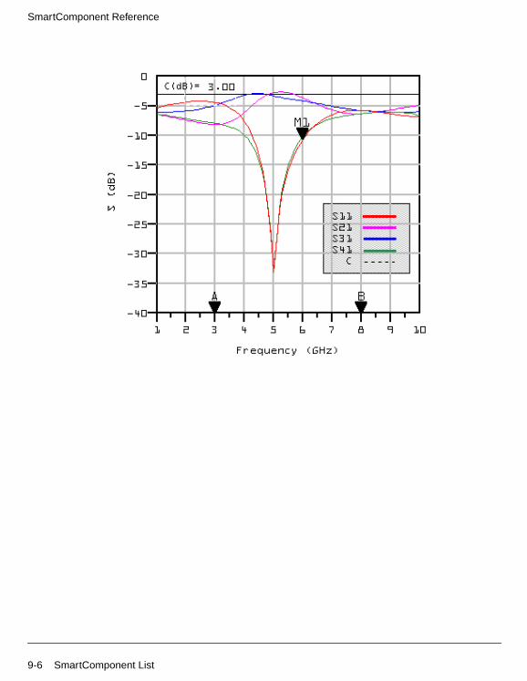
SmartComponent Reference
9-6 SmartComponent List

CLCoupler (Coupled-Line Coupler)
Symbol
Summary
A coupled-line coupler outputs from the coupled port (pin 4) a fraction of the power presented atthe input (pin 1). The remainder of the power is passed through to the output port (pin 2). Thecoupling coefficient specifies the ratio of the input power to the coupled power (P1/P4). The
remaining port is isolated, although the isolation is often similar in value to the couplingcoefficient for microstrip realizations.
Note A SmartComponent subnetwork is empty until the Design Assistant is used to generate thedesign. Refer to Chapter 4, Design Assistant.
Parameters
Subst = microstrip substrate name
F = center frequency, in hertz
C = coupling coefficient, in dB
Zo = characteristic impedance, in ohms
Delta = length added to branches for tuning performance
Palette
Passive Circuit - Couplers
Available Automated-Assistants
Design Assistant, Simulation Assistant, Optimization Assistant, Display Assistant
Design Assistant Usage
For general information, refer to Chapter 4, Design Assistant.
1. The coupling coefficient must be positive and greater than 3 dB. Best results are obtainedfor weak couplings of roughly 10 dB or more (C >10dB). Choosing the coupling coefficienttoo small may require a spacing between the coupled lines too small to realize.
SmartComponent List 9-7

SmartComponent Reference
2. For a more detailed discussion of this device, see: D. M. Pozar, Microwave Engineering,2nd Edition, John Wiley & Sons: New York, 1998, pp. 383-394.
Simulation Assistant Usage
For general information, refer to Chapter 5, Simulation Assistant.
Optimization Assistant Usage
For general information, refer to Chapter 6, Optimization Assistant.
The optimization minimizes the absolute difference between S41 in dB and the specified couplingcoefficient at the design center frequency by changing the length of the coupled-line section.
Display Assistant Usage
For general information, refer to Chapter 7, Display Assistant.
Example
A coupled-line coupler was designed for a center frequency of 5 GHz with 20 dB of coupling.Tuning using the Optimization Assistant yielded a value of Delta =-1.087 mil.
9-8 SmartComponent List
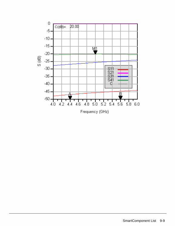
SmartComponent List 9-9
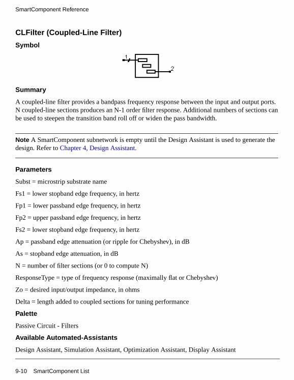
SmartComponent Reference
CLFilter (Coupled-Line Filter)
Symbol
Summary
A coupled-line filter provides a bandpass frequency response between the input and output ports.N coupled-line sections produces an N-1 order filter response. Additional numbers of sections canbe used to steepen the transition band roll off or widen the pass bandwidth.
Note A SmartComponent subnetwork is empty until the Design Assistant is used to generate thedesign. Refer to Chapter 4, Design Assistant.
Parameters
Subst = microstrip substrate name
Fs1 = lower stopband edge frequency, in hertz
Fp1 = lower passband edge frequency, in hertz
Fp2 = upper passband edge frequency, in hertz
Fs2 = lower stopband edge frequency, in hertz
Ap = passband edge attenuation (or ripple for Chebyshev), in dB
As = stopband edge attenuation, in dB
N = number of filter sections (or 0 to compute N)
ResponseType = type of frequency response (maximally flat or Chebyshev)
Zo = desired input/output impedance, in ohms
Delta = length added to coupled sections for tuning performance
Palette
Passive Circuit - Filters
Available Automated-Assistants
Design Assistant, Simulation Assistant, Optimization Assistant, Display Assistant
9-10 SmartComponent List
Design Assistant Usage
For general information, refer to Chapter 4, Design Assistant.
1. Because of the heavy computational burden in determining the line parameters, a brief delaywill occur for the design.
2. For a Chebyshev (equal ripple) frequency response, ripple levels greater than about 1 dB arenot recommended. Exceeding this value will typically deform the shape of the passbandcharacteristics.
3. If N is zero, the number of filter sections will be computed from the frequency/attenuationinformation. If N is non-zero, the design will use the frequency/attenuation parameters onlyfor determining the design center frequency.
4. For a more detailed discussion of this device, see D. M. Pozar, Microwave Engineering, 2ndEdition, John Wiley & Sons: New York, 1998, pp. 477-485.
Simulation Assistant Usage
For general information, refer to Chapter 5, Simulation Assistant.
Optimization Assistant Usage
For general information, refer to Chapter 6, Optimization Assistant.
The optimization minimizes the absolute difference between S21 in dB and the specified passbandedge attenuation (which equals the ripple for Chebyshev response) at the passband edgefrequencies. Because only the line lengths are changed, this tuning will typically center theresponse within the specified passband. More advanced shaping of the passband response can beaccomplished by manually tuning the widths and spacings of the coupled filter sections.
Display Assistant Usage
For general information, refer to Chapter 7, Display Assistant.
Example
A coupled-line filter was designed for a maximally flat response with the 3 dB passband edgefrequencies at 2 GHz and 2.4 GHz respectively. The design required 4 coupled-line sections.Tuning using the Optimization Assistant yielded a value of Delta = -5.244 mil.
SmartComponent List 9-11
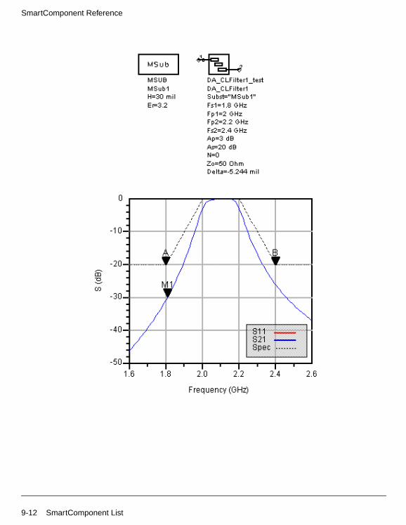
SmartComponent Reference
9-12 SmartComponent List

CMFilter (Comb-Line Filter)
Symbol
Summary
A comb-line filter provides a bandpass frequency response between the input and output ports. Ncoupled-line sections produce an N-1 order filter response. Additional numbers of sections can beused to steepen the transition band roll off or widen the pass bandwidth.
Note A SmartComponent subnetwork is empty until the Design Assistant is used to generate thedesign. Refer to Chapter 4, Design Assistant.
Parameters
Subst = microstrip substrate name
Fs1 = lower stopband edge frequency, in hertz
Fp1 = lower passband edge frequency, in hertz
Fp2 = upper passband edge frequency, in hertz
Fs2 = lower stopband edge frequency, in hertz
Ap = passband edge attenuation (or ripple for Chebyshev), in dB
As = stopband edge attenuation, in dB
N = number of filter sections (or 0 to compute N)
ResponseType = type of frequency response (maximally flat or Chebyshev)
Zo = desired input/output impedance, in ohms
Lelec = electrical length of filter resonators (the units of Leclec are in fractions of a wavelengthi.e., 0.25 = 1/4 wavelength)
ya = normalized interior resonator admittance (0 < ya < 1)
CouplingType = type of input/output coupling (coupled line or tapped line transformer)
Delta = length added to coupled sections for tuning performance
SmartComponent List 9-13

SmartComponent Reference
Palette
Passive Circuit - Filters
Available Automated-Assistants
Design Assistant, Simulation Assistant, Optimization Assistant, Display Assistant
Design Assistant Usage
For general information, refer to Chapter 4, Design Assistant.
1. Because of the heavy computational burden in determining the line parameters, a brief delaywill occur for the design.
2. A two-layer substrate must be used for this topology.
3. For a Chebyshev (equal ripple) frequency response, ripple levels greater than about 1 dB arenot recommended. Exceeding this value will typically deform the shape of the passbandcharacteristics.
4. If N is zero, the number of filter sections will be computed from the frequency/attenuationinformation. If N is non-zero, the design will use the frequency/attenuation parameters onlyfor determining the design center frequency.
5. Using a CouplingType of “Coupled Line Transformer Input” will use an extra coupled linesection on the inputs and outputs to feed the device. Choosing “Tapped Line TransformerInput” will bring the feedline directly into the first resonator.
6. For a more detailed discussion of this device, refer to: Matthaei, Young and Jones,Microwave Filters, Impedance-Matching Networks, and Coupling Structures, ArtechHouse, 1980, pp. 497.
Simulation Assistant Usage
For general information, refer to Chapter 5, Simulation Assistant.
Optimization Assistant Usage
For general information, refer to Chapter 6, Optimization Assistant.
The optimization minimizes the absolute difference between S21 in dB and the specified passbandedge attenuation (which equals the ripple for Chebyshev response) at the passband edgefrequencies. Because only the line lengths are changed, this tuning will typically center theresponse within the specified passband. More advanced shaping of the passband response can beaccomplished by manually tuning the widths and spacings of the coupled filter sections.
Display Assistant Usage
9-14 SmartComponent List
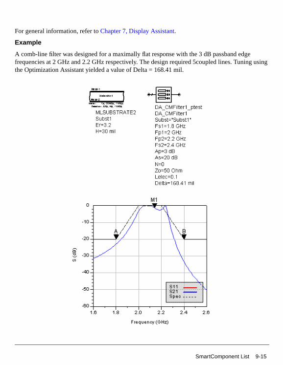
For general information, refer to Chapter 7, Display Assistant.
Example
A comb-line filter was designed for a maximally flat response with the 3 dB passband edgefrequencies at 2 GHz and 2.2 GHz respectively. The design required 5coupled lines. Tuning usingthe Optimization Assistant yielded a value of Delta = 168.41 mil.
SmartComponent List 9-15

SmartComponent Reference
DSMatch (Double-Stub Match)
Symbol
Summary
A double-stub matching network matches a complex load impedance (Zload) to a desired complexinput impedance (Zin) using two shunt stubs and a connecting line.
Note A SmartComponent subnetwork is empty until the Design Assistant is used to generate thedesign. Refer to Chapter 4, Design Assistant.
Parameters
Subst = microstrip substrate name
F = center frequency, in hertz
Zin = desired complex input impedance, in ohms
Zload = complex load impedance to match, in ohms
Zstub1 = characteristic impedance of stub line 1 (nearest input), in ohms
Zstub2 = characteristic impedance of stub line 2 (nearest output), in ohms
Zline = characteristic impedance of line between stubs, in ohms
Zfeed1 = characteristic impedance of line connected to port 1, in ohms
Zfeed2 = characteristic impedance of line connected to port 2, in ohms
Stub1Type = stub 1 type (open or short circuit)
Stub2Type = stub 2 type (open or short circuit)
Delta = length added to stubs for tuning performance
Palette
Passive Circuit - Matching
Available Automated-Assistants
9-16 SmartComponent List
Design Assistant, Simulation Assistant, Optimization Assistant, Display Assistant
Design Assistant Usage
For general information, refer to Chapter 4, Design Assistant.
1. An impedance match can be realized using any combination of stub types, although somecombinations may be more realizable.
2. Zfeed1 and Zfeed2 are used simply to ensure that the input and output legs of the microstriptee components are of the proper width.
3. The length of the line between the stubs is nominally chosen to be an eighth of a linewavelength. However, if this will not realize the match, the length of line is computed suchthat the rotated circle on the Smith chart encloses the load admittance.
4. MTEE component width constraint violations will be avoided generally by choosing similarcharacteristic impedances for the line, stub, and feed.
5. Since two solutions are possible, the solution that results in the smallest length of stub 1 ischosen. For example, if stub 1 is open circuited, the solution for which stub 1 must realize acapacitive reactance is chosen.
6. For a more detailed discussion of this device, see: D. M. Pozar, Microwave Engineering,2nd Edition, John Wiley & Sons: New York, 1998, pp. 266-271.
Simulation Assistant Usage
For general information, refer to Chapter 5, Simulation Assistant.
The input port termination is set to the conjugate of Zin so that the ideal input reflection coefficientwill be zero. The output port termination is set to Zload.
Optimization Assistant Usage
For general information, refer to Chapter 6, Optimization Assistant.
The optimization minimizes the value of S11 (referenced to the conjugate of Zin) at the designcenter frequency by changing the length of the stubs. Both stubs are tuned by the same length.
Display Assistant Usage
For general information, refer to Chapter 7, Display Assistant.
Example
A double-stub matching network was designed to match a load impedance of 100 - j30 ohms to a50 ohm line at a center frequency of 5 GHz with open circuited stubs. Tuning using theOptimization Assistant yielded a value of Delta =-31.633 mil.
SmartComponent List 9-17

SmartComponent Reference
9-18 SmartComponent List
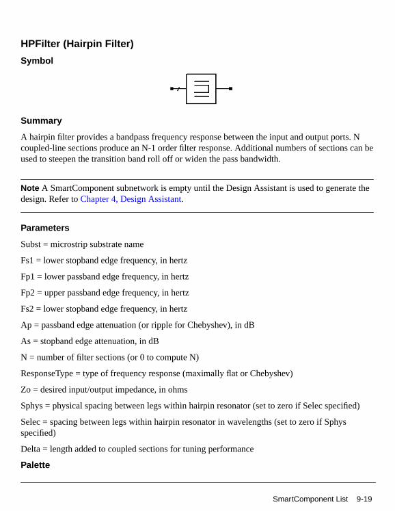
HPFilter (Hairpin Filter)
Symbol
Summary
A hairpin filter provides a bandpass frequency response between the input and output ports. Ncoupled-line sections produce an N-1 order filter response. Additional numbers of sections can beused to steepen the transition band roll off or widen the pass bandwidth.
Note A SmartComponent subnetwork is empty until the Design Assistant is used to generate thedesign. Refer to Chapter 4, Design Assistant.
Parameters
Subst = microstrip substrate name
Fs1 = lower stopband edge frequency, in hertz
Fp1 = lower passband edge frequency, in hertz
Fp2 = upper passband edge frequency, in hertz
Fs2 = lower stopband edge frequency, in hertz
Ap = passband edge attenuation (or ripple for Chebyshev), in dB
As = stopband edge attenuation, in dB
N = number of filter sections (or 0 to compute N)
ResponseType = type of frequency response (maximally flat or Chebyshev)
Zo = desired input/output impedance, in ohms
Sphys = physical spacing between legs within hairpin resonator (set to zero if Selec specified)
Selec = spacing between legs within hairpin resonator in wavelengths (set to zero if Sphysspecified)
Delta = length added to coupled sections for tuning performance
Palette
SmartComponent List 9-19
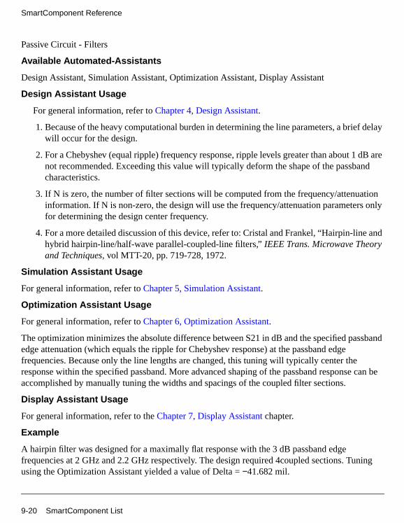
SmartComponent Reference
Passive Circuit - Filters
Available Automated-Assistants
Design Assistant, Simulation Assistant, Optimization Assistant, Display Assistant
Design Assistant Usage
For general information, refer to Chapter 4, Design Assistant.
1. Because of the heavy computational burden in determining the line parameters, a brief delaywill occur for the design.
2. For a Chebyshev (equal ripple) frequency response, ripple levels greater than about 1 dB arenot recommended. Exceeding this value will typically deform the shape of the passbandcharacteristics.
3. If N is zero, the number of filter sections will be computed from the frequency/attenuationinformation. If N is non-zero, the design will use the frequency/attenuation parameters onlyfor determining the design center frequency.
4. For a more detailed discussion of this device, refer to: Cristal and Frankel, “Hairpin-line andhybrid hairpin-line/half-wave parallel-coupled-line filters,” IEEE Trans. Microwave Theoryand Techniques, vol MTT-20, pp. 719-728, 1972.
Simulation Assistant Usage
For general information, refer to Chapter 5, Simulation Assistant.
Optimization Assistant Usage
For general information, refer to Chapter 6, Optimization Assistant.
The optimization minimizes the absolute difference between S21 in dB and the specified passbandedge attenuation (which equals the ripple for Chebyshev response) at the passband edgefrequencies. Because only the line lengths are changed, this tuning will typically center theresponse within the specified passband. More advanced shaping of the passband response can beaccomplished by manually tuning the widths and spacings of the coupled filter sections.
Display Assistant Usage
For general information, refer to the Chapter 7, Display Assistant chapter.
Example
A hairpin filter was designed for a maximally flat response with the 3 dB passband edgefrequencies at 2 GHz and 2.2 GHz respectively. The design required 4coupled sections. Tuningusing the Optimization Assistant yielded a value of Delta = −41.682 mil.
9-20 SmartComponent List
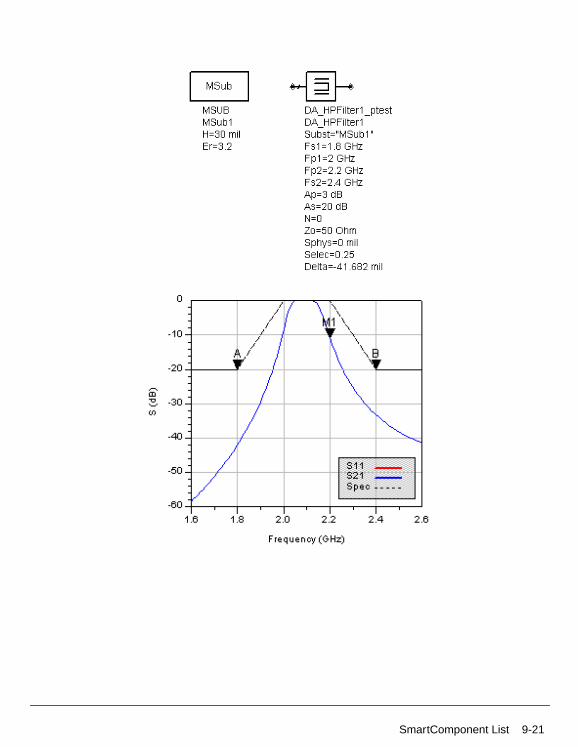
SmartComponent List 9-21

SmartComponent Reference
IDFilter (Interdigital Filter)
Symbol
Summary
An interdigital filter provides a bandpass frequency response between the input and output ports. Ncoupled-line sections produce an N-1 order filter response. Additional numbers of sections can beused to steepen the transition band roll off or widen the pass bandwidth.
Note A SmartComponent subnetwork is empty until the Design Assistant is used to generate thedesign. Refer to Chapter 4, Design Assistant.
Parameters
Subst = microstrip substrate name
Fs1 = lower stopband edge frequency, in hertz
Fp1 = lower passband edge frequency, in hertz
Fp2 = upper passband edge frequency, in hertz
Fs2 = lower stopband edge frequency, in hertz
Ap = passband edge attenuation (or ripple for Chebyshev), in dB
As = stopband edge attenuation, in dB
N = number of filter sections (or 0 to compute N)
ResponseType = type of frequency response (maximally flat or Chebyshev)
Zo = desired input/output impedance, in ohms
ya = normalized interior resonator admittance (0 < ya < 1)
CouplingType = type of input/output coupling (coupled line or tapped line transformer)
Delta = length added to coupled sections for tuning performance
Palette
Passive Circuit - Filters
9-22 SmartComponent List

Available Automated-Assistants
Design Assistant, Simulation Assistant, Optimization Assistant, Display Assistant
Design Assistant Usage
For general information, refer to Chapter 4, Design Assistant.
1. Because of the heavy computational burden in determining the line parameters, a brief delaywill occur for the design.
2. A two-layer substrate must be used for this topology.
3. For a Chebyshev (equal ripple) frequency response, ripple levels greater than about 1 dB arenot recommended. Exceeding this value will typically deform the shape of the passbandcharacteristics.
4. If N is zero, the number of filter sections will be computed from the frequency/attenuationinformation. If N is non-zero, the design will use the frequency/attenuation parameters onlyfor determining the design center frequency.
5. Using a CouplingType of “Coupled Line Transformer Input” will use an extra coupled linesection on the inputs and outputs to feed the device. Choosing “Tapped Line TransformerInput” will bring the feedline directly into the first resonator.
6. For a more detailed discussion of this device, refer to: Matthaei, Young and Jones,Microwave Filters, Impedance-Matching Networks, and Coupling Structures, ArtechHouse, 1980, pp. 614.
Simulation Assistant Usage
For general information, refer to Chapter 5, Simulation Assistant.
Optimization Assistant Usage
For general information, refer to Chapter 6, Optimization Assistant
The optimization minimizes the absolute difference between S21 in dB and the specified passbandedge attenuation (which equals the ripple for Chebyshev response) at the passband edgefrequencies. Because only the line lengths are changed, this tuning will typically center theresponse within the specified passband. More advanced shaping of the passband response can beaccomplished by manually tuning the widths and spacings of the coupled filter sections.
Display Assistant Usage
For general information, refer to Chapter 7, Display Assistant.
Example
SmartComponent List 9-23
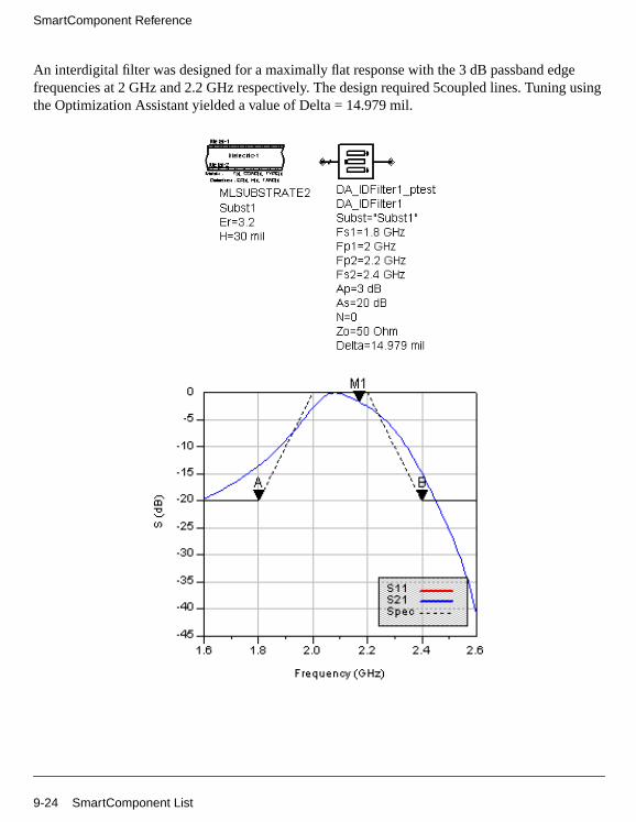
SmartComponent Reference
An interdigital filter was designed for a maximally flat response with the 3 dB passband edgefrequencies at 2 GHz and 2.2 GHz respectively. The design required 5coupled lines. Tuning usingthe Optimization Assistant yielded a value of Delta = 14.979 mil.
9-24 SmartComponent List
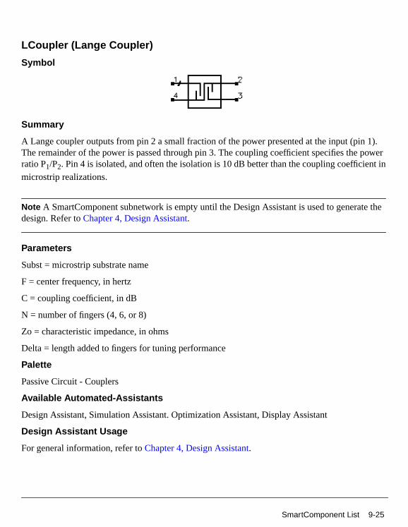
LCoupler (Lange Coupler)
Symbol
Summary
A Lange coupler outputs from pin 2 a small fraction of the power presented at the input (pin 1).The remainder of the power is passed through pin 3. The coupling coefficient specifies the powerratio P1/P2. Pin 4 is isolated, and often the isolation is 10 dB better than the coupling coefficient in
microstrip realizations.
Note A SmartComponent subnetwork is empty until the Design Assistant is used to generate thedesign. Refer to Chapter 4, Design Assistant.
Parameters
Subst = microstrip substrate name
F = center frequency, in hertz
C = coupling coefficient, in dB
N = number of fingers (4, 6, or 8)
Zo = characteristic impedance, in ohms
Delta = length added to fingers for tuning performance
Palette
Passive Circuit - Couplers
Available Automated-Assistants
Design Assistant, Simulation Assistant. Optimization Assistant, Display Assistant
Design Assistant Usage
For general information, refer to Chapter 4, Design Assistant.
SmartComponent List 9-25
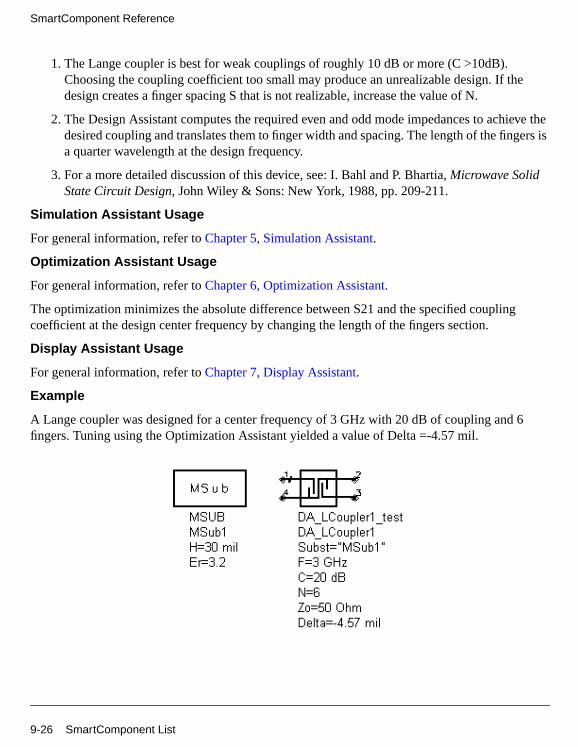
SmartComponent Reference
1. The Lange coupler is best for weak couplings of roughly 10 dB or more (C >10dB).Choosing the coupling coefficient too small may produce an unrealizable design. If thedesign creates a finger spacing S that is not realizable, increase the value of N.
2. The Design Assistant computes the required even and odd mode impedances to achieve thedesired coupling and translates them to finger width and spacing. The length of the fingers isa quarter wavelength at the design frequency.
3. For a more detailed discussion of this device, see: I. Bahl and P. Bhartia, Microwave SolidState Circuit Design, John Wiley & Sons: New York, 1988, pp. 209-211.
Simulation Assistant Usage
For general information, refer to Chapter 5, Simulation Assistant.
Optimization Assistant Usage
For general information, refer to Chapter 6, Optimization Assistant.
The optimization minimizes the absolute difference between S21 and the specified couplingcoefficient at the design center frequency by changing the length of the fingers section.
Display Assistant Usage
For general information, refer to Chapter 7, Display Assistant.
Example
A Lange coupler was designed for a center frequency of 3 GHz with 20 dB of coupling and 6fingers. Tuning using the Optimization Assistant yielded a value of Delta =-4.57 mil.
9-26 SmartComponent List

SmartComponent List 9-27
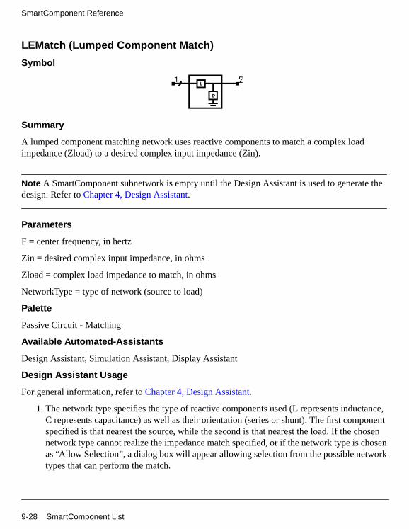
SmartComponent Reference
LEMatch (Lumped Component Match)
Symbol
Summary
A lumped component matching network uses reactive components to match a complex loadimpedance (Zload) to a desired complex input impedance (Zin).
Note A SmartComponent subnetwork is empty until the Design Assistant is used to generate thedesign. Refer to Chapter 4, Design Assistant.
Parameters
F = center frequency, in hertz
Zin = desired complex input impedance, in ohms
Zload = complex load impedance to match, in ohms
NetworkType = type of network (source to load)
Palette
Passive Circuit - Matching
Available Automated-Assistants
Design Assistant, Simulation Assistant, Display Assistant
Design Assistant Usage
For general information, refer to Chapter 4, Design Assistant.
1. The network type specifies the type of reactive components used (L represents inductance,C represents capacitance) as well as their orientation (series or shunt). The first componentspecified is that nearest the source, while the second is that nearest the load. If the chosennetwork type cannot realize the impedance match specified, or if the network type is chosenas “Allow Selection”, a dialog box will appear allowing selection from the possible networktypes that can perform the match.
9-28 SmartComponent List
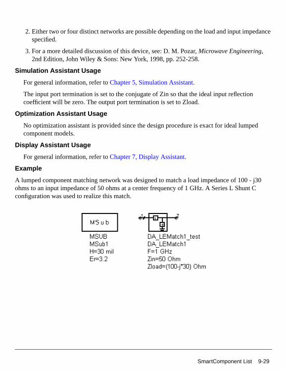
2. Either two or four distinct networks are possible depending on the load and input impedancespecified.
3. For a more detailed discussion of this device, see: D. M. Pozar, Microwave Engineering,2nd Edition, John Wiley & Sons: New York, 1998, pp. 252-258.
Simulation Assistant Usage
For general information, refer to Chapter 5, Simulation Assistant.
The input port termination is set to the conjugate of Zin so that the ideal input reflectioncoefficient will be zero. The output port termination is set to Zload.
Optimization Assistant Usage
No optimization assistant is provided since the design procedure is exact for ideal lumpedcomponent models.
Display Assistant Usage
For general information, refer to Chapter 7, Display Assistant.
Example
A lumped component matching network was designed to match a load impedance of 100 - j30ohms to an input impedance of 50 ohms at a center frequency of 1 GHz. A Series L Shunt Cconfiguration was used to realize this match.
SmartComponent List 9-29

SmartComponent Reference
9-30 SmartComponent List

MBend (Microstrip Bend Component)
Symbol
Summary
MBend designs a microstrip bend given the substrate, desired characteristic impedance, and bendproperties. The design will realize the native MBEND, MBEND2, or MBEND3 components.
Note A SmartComponent subnetwork is empty until the Design Assistant is used to generate thedesign. Refer to Chapter 4, Design Assistant.
Parameters
Subst = microstrip substrate name
F = design frequency, in hertz
Zo = desired characteristic impedance, in ohms
BendType = type of bend
Angle = angle of bend (for arbitrary angle/miter bend)
M = miter fraction (for arbitrary angle/miter bend)
Palette
Passive Circuit - Lines
Available Automated-Assistants
Design Assistant
Design Assistant Usage
For general information, refer to Chapter 4, Design Assistant.
1. Since the design uses the models inherent to ADS to compute the line width, there is noneed for a dedicated Simulation Assistant, Optimization Assistant, or Display Assistant.
SmartComponent List 9-31

SmartComponent Reference
2. BendType can be Arbitrary Angle/Miter (MBEND), 90 Degree/Miter (MBEND2), or 90Degree/Optimal Miter (MBEND3). The parameters Angle and M are only used for MBENDrealizations. refer to the discussion of these components in the ADS Microstrip Componentsdocumentation for a more detailed description.
9-32 SmartComponent List

MBStub (Microstrip Butterfly Radial Stub)
Symbol
Summary
MBStub designs a microstrip butterfly radial stub given the substrate, desired input reactance, andstub dimensions.
Note A SmartComponent subnetwork is empty until the Design Assistant is used to generate thedesign. Refer to Chapter 4, Design Assistant.
Parameters
Subst = microstrip substrate name
F = design frequency, in hertz
Xin = desired input reactance, in ohms (only one of Xin, Cin, and Lin can be non-zero)
Cin = desired input capacitance, in farads (only one of Xin, Cin, and Lin can be non-zero)
Lin = desired input inductance, in henries (only one of Xin, Cin, and Lin can be non-zero)
W = width of feed line (set to zero if Z specified)
Z = characteristic impedance of feed line (set to zero if W specified)
Angle = subtended angle of circular sector
d = insertion depth of circular sector in feed line
Delta = length added to stub for tuning performance
Palette
Passive Circuit - Lines
Available Automated-Assistants
Design Assistant, Simulation Assistant, Optimization Assistant, Display Assistant
Design Assistant Usage
SmartComponent List 9-33
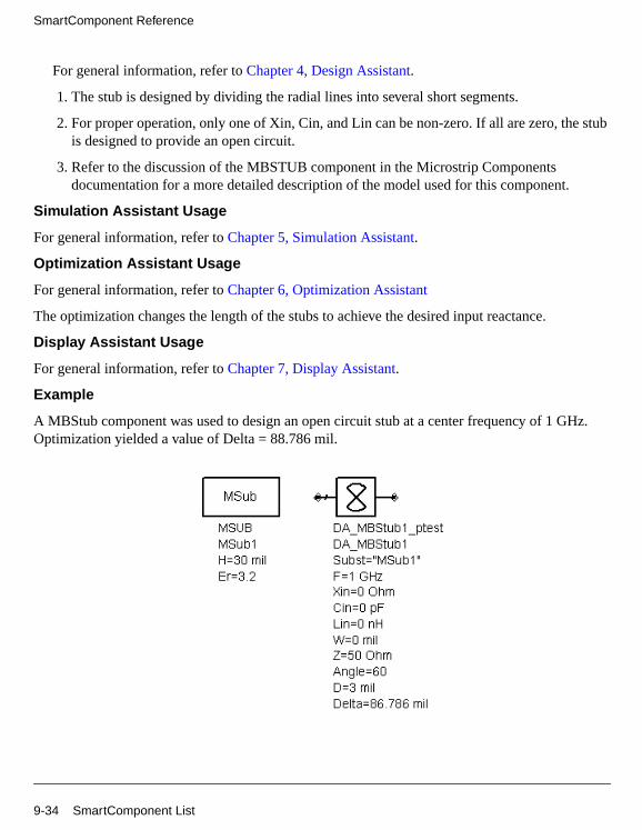
SmartComponent Reference
For general information, refer to Chapter 4, Design Assistant.
1. The stub is designed by dividing the radial lines into several short segments.
2. For proper operation, only one of Xin, Cin, and Lin can be non-zero. If all are zero, the stubis designed to provide an open circuit.
3. Refer to the discussion of the MBSTUB component in the Microstrip Componentsdocumentation for a more detailed description of the model used for this component.
Simulation Assistant Usage
For general information, refer to Chapter 5, Simulation Assistant.
Optimization Assistant Usage
For general information, refer to Chapter 6, Optimization Assistant
The optimization changes the length of the stubs to achieve the desired input reactance.
Display Assistant Usage
For general information, refer to Chapter 7, Display Assistant.
Example
A MBStub component was used to design an open circuit stub at a center frequency of 1 GHz.Optimization yielded a value of Delta = 88.786 mil.
9-34 SmartComponent List
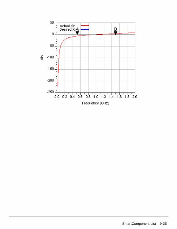
SmartComponent List 9-35

SmartComponent Reference
MCFil (Microstrip Coupled Filter Component)
Symbol
Summary
MCFil designs a microstrip coupled filter component given the substrate, desired even- andodd-mode characteristic impedances, and physical or electrical length.
Note A SmartComponent subnetwork is empty until the Design Assistant is used to generate thedesign. Refer to Chapter 4, Design Assistant.
Parameters
Subst = microstrip substrate name
F = design frequency, in hertz
Zoe = desired even-mode characteristic impedance, in ohms
Zoo = desired odd-mode characteristic impedance, in ohms
Zo1 = characteristic impedance of input line at port 1, in ohms
Zo2 = characteristic impedance of input line at port 2, in ohms
Lphys = physical line length (set to zero if Lelec specified)
Lelec = line length in wavelengths (set to zero if Lphys specified)
Palette
Passive Circuit - Lines
Available Automated-Assistants
Design Assistant
Design Assistant Usage
For general information, refer to Chapter 4, Design Assistant.
9-36 SmartComponent List

1. Since the design uses the models inherent to ADS to compute the line width, there is noneed for a dedicated Simulation Assistant, Optimization Assistant, or Display Assistant.
2. For proper operation, either Lphys or Lelec must be zero.
3. Zo1 and Zo2 specify the impedance of the lines attached to this component and are providedto ensure proper pin location in the layout. refer to the discussion of the MCFIL componentin the Microstrip Components documentation for a more detailed description of the modelused for this component.
SmartComponent List 9-37

SmartComponent Reference
MCLine (Microstrip Coupled Line Component)
Symbol
Summary
MCLine designs a microstrip coupled line component given the substrate, desired even- andodd-mode characteristic impedances, and physical or electrical length.
Note A SmartComponent subnetwork is empty until the Design Assistant is used to generate thedesign. Refer to Chapter 4, Design Assistant.
Parameters
Subst = microstrip substrate name
F = design frequency, in hertz
Zoe = desired even-mode characteristic impedance, in ohms
Zoo = desired odd-mode characteristic impedance, in ohms
Zo1 = characteristic impedance of input line at port 1, in ohms
Zo2 = characteristic impedance of input line at port 2, in ohms
Zo3 = characteristic impedance of input line at port 3, in ohms
Zo4 = characteristic impedance of input line at port 4, in ohms
Lphys = physical line length (set to zero if Lelec specified)
Lelec = line length in wavelengths (set to zero if Lphys specified)
Palette
Passive Circuit - Lines
Available Automated-Assistants
Design Assistant
Design Assistant Usage
9-38 SmartComponent List

For general information, refer to Chapter 4, Design Assistant
1. Since the design uses the models inherent to ADS to compute the line width, there is noneed for a dedicated Simulation Assistant, Optimization Assistant, or Display Assistant.
2. For proper operation, either Lphys or Lelec must be zero.
3. Zo1 through Zo4 specify the impedance of the lines attached to this component and areprovided to ensure proper pin location in the layout. refer to the discussion of the MCFILcomponent in the Microstrip Components documentation for a more detailed description ofthe model used for this component.
SmartComponent List 9-39

SmartComponent Reference
MCorn (Microstrip Corner Component)
Symbol
Summary
MCorn designs a microstrip corner component given the substrate and characteristic impedance ofthe input and output lines.
Note A SmartComponent subnetwork is empty until the Design Assistant is used to generate thedesign. Refer to Chapter 4, Design Assistant.
Parameters
Subst = microstrip substrate name
F = design frequency, in hertz
Zo = desired characteristic impedance, in ohms
Palette
Passive Circuit - Lines
Available Automated-Assistants
Design Assistant
Design Assistant Usage
For general information, refer to Chapter 4, Design Assistant.
1. Since the design uses the models inherent to ADS to compute the line width, there is noneed for a dedicated Simulation Assistant, Optimization Assistant, or Display Assistant.
2. Refer to the discussion of the MCORN component in the Microstrip Componentsdocumentation for a more detailed description of the model used for this component.
9-40 SmartComponent List

MCross (Microstrip Cross Component)
Symbol
Summary
MCross designs a microstrip cross given the substrate, desired characteristic impedance on eachport, and bend properties. The design will realize the native MCURVE and MCURVE2components.
Note A SmartComponent subnetwork is empty until the Design Assistant is used to generate thedesign. Refer to Chapter 4, Design Assistant.
Parameters
Subst = microstrip substrate name
F = design frequency, in hertz
Z1 = characteristic impedance of port 1, in ohms
Z2 = characteristic impedance of port 2, in ohms
Z3 = characteristic impedance of port 3, in ohms
Z4 = characteristic impedance of port 4, in ohms
Palette
Passive Circuit - Lines
Available Automated-Assistants
Design Assistant
Design Assistant Usage
For general information, refer to Chapter 4, Design Assistant.
1. Since the design uses the models inherent to ADS to compute the line width, there is noneed for a dedicated Simulation Assistant, Optimization Assistant, or Display Assistant.
SmartComponent List 9-41

SmartComponent Reference
2. Refer to the discussion of the MCROSS component in the Microstrip Componentsdocumentation for a detailed description of this component.
9-42 SmartComponent List

MCurve (Microstrip Curve Component)
Symbol
Summary
MBend designs a microstrip bend given the substrate, desired characteristic impedance, and bendproperties. The design will realize the native MCURVE and MCURVE2 components.
Note A SmartComponent subnetwork is empty until the Design Assistant is used to generate thedesign. Refer to Chapter 4, Design Assistant.
Parameters
Subst = microstrip substrate name
F = design frequency, in hertz
Zo = desired characteristic impedance, in ohms
Angle = angle of curve
Radius = radius of curvature (set to zero if Lelec specified)
Lelec = curve length in wavelengths (set to zero if Radius specified)
CurveType = type of curve
Nmode = number of modes (for Waveguide Model)
Palette
Passive Circuit - Lines
Available Automated-Assistants
Design Assistant
Design Assistant Usage
For general information, refer to Chapter 4, Design Assistant.
SmartComponent List 9-43

SmartComponent Reference
1. Since the design uses the models inherent to ADS to compute the line width, there is noneed for a dedicated Simulation Assistant, Optimization Assistant, or Display Assistant.
2. Either Lelec or Radius must be zero for proper operation.
3. BendType can be Transmission Line Model (MCURVE) or Magnetic Wall WaveguideModel (MCURVE2). The parameter Nmode is used only for MCURVE2. refer to the to thediscussion of these components in the Microstrip Components documentation for a moredetailed description.
9-44 SmartComponent List
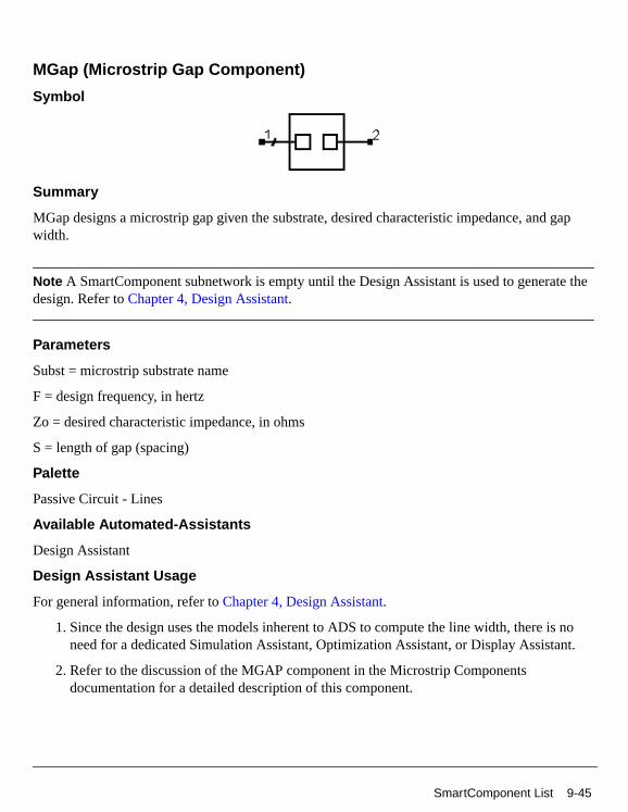
MGap (Microstrip Gap Component)
Symbol
Summary
MGap designs a microstrip gap given the substrate, desired characteristic impedance, and gapwidth.
Note A SmartComponent subnetwork is empty until the Design Assistant is used to generate thedesign. Refer to Chapter 4, Design Assistant.
Parameters
Subst = microstrip substrate name
F = design frequency, in hertz
Zo = desired characteristic impedance, in ohms
S = length of gap (spacing)
Palette
Passive Circuit - Lines
Available Automated-Assistants
Design Assistant
Design Assistant Usage
For general information, refer to Chapter 4, Design Assistant.
1. Since the design uses the models inherent to ADS to compute the line width, there is noneed for a dedicated Simulation Assistant, Optimization Assistant, or Display Assistant.
2. Refer to the discussion of the MGAP component in the Microstrip Componentsdocumentation for a detailed description of this component.
SmartComponent List 9-45
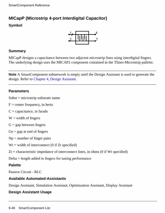
SmartComponent Reference
MICapP (Microstrip 4-port Interdigital Capacitor)
Symbol
Summary
MICapP designs a capacitance between two adjacent microstrip lines using interdigital fingers.The underlying design uses the MICAP2 component contained in the Tlines-Microstrip pallette.
Note A SmartComponent subnetwork is empty until the Design Assistant is used to generate thedesign. Refer to Chapter 4, Design Assistant.
Parameters
Subst = microstrip substrate name
F = center frequency, in hertz
C = capacitance, in farads
W = width of fingers
G = gap between fingers
Ge = gap at end of fingers
Np = number of finger pairs
Wt = width of interconnect (0 if Zt specified)
Zt = characteristic impedance of interconnect lines, in ohms (0 if Wt specified)
Delta = length added to fingers for tuning performance
Palette
Passive Circuit - RLC
Available Automated-Assistants
Design Assistant, Simulation Assistant, Optimization Assistant, Display Assistant
Design Assistant Usage
9-46 SmartComponent List

For general information, refer to Chapter 4, Design Assistant.
1. The design is accomplished using a simple model that specifies the length required toachieve the capacitance C at the design center frequency given the remaining physicalparameters. If the computed length is unreasonable, decreasing or increasing the gap G willincrease or decrease the capacitance, respectively and therefore allow altering of the length.
2. Both Wt and Zt specify the properties of the interconnect line. For proper operation, makesure that only one of these parameters is non-zero.
3. For more detailed discussion of the parameters W, G, Ge, Np, and Wt, please refer to thediscussion of MICAP2 in the Microstrip Components documentation.
Simulation Assistant Usage
For general information, refer to Chapter 5, Simulation Assistant.
Optimization Assistant Usage
For general information, refer to Chapter 6, Optimization Assistant.
The Optimization Assistant tunes the length of the fingers to achieve the desired capacitance.Because of the simple design approach used, it is often wise to first roughly tune the design withinthe Simulation Assistant and subsequently use the optimizer to perform the fine tuning.
Display Assistant Usage
For general information, refer to Chapter 7, Display Assistant.
Example
A MICapP component was used to design a 1 pF capacitance between two 50 ohm lines at a centerfrequency of 5 GHz. Optimization yielded a value of Delta = -22.19 mil.
SmartComponent List 9-47
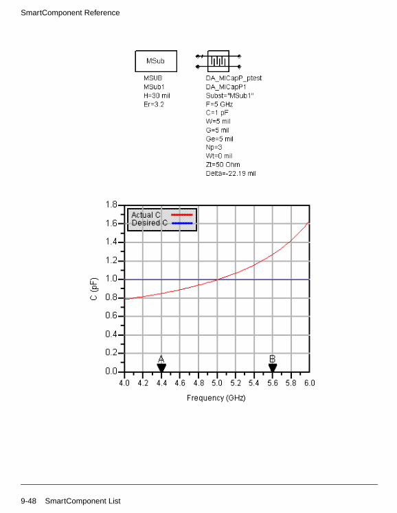
SmartComponent Reference
9-48 SmartComponent List
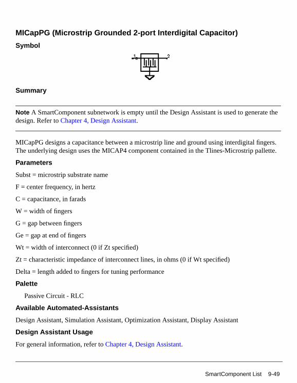
MICapPG (Microstrip Grounded 2-port Interdigital Capacitor)
Symbol
Summary
Note A SmartComponent subnetwork is empty until the Design Assistant is used to generate thedesign. Refer to Chapter 4, Design Assistant.
MICapPG designs a capacitance between a microstrip line and ground using interdigital fingers.The underlying design uses the MICAP4 component contained in the Tlines-Microstrip pallette.
Parameters
Subst = microstrip substrate name
F = center frequency, in hertz
C = capacitance, in farads
W = width of fingers
G = gap between fingers
Ge = gap at end of fingers
Wt = width of interconnect (0 if Zt specified)
Zt = characteristic impedance of interconnect lines, in ohms (0 if Wt specified)
Delta = length added to fingers for tuning performance
Palette
Passive Circuit - RLC
Available Automated-Assistants
Design Assistant, Simulation Assistant, Optimization Assistant, Display Assistant
Design Assistant Usage
For general information, refer to Chapter 4, Design Assistant.
SmartComponent List 9-49
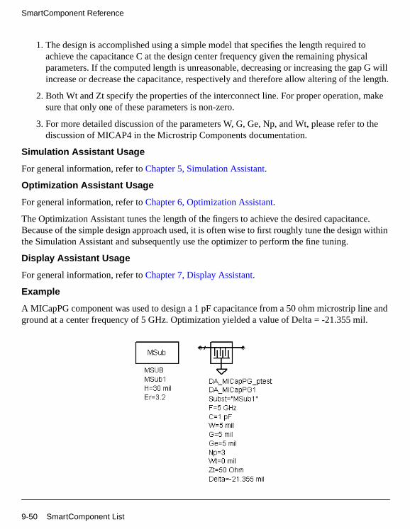
SmartComponent Reference
1. The design is accomplished using a simple model that specifies the length required toachieve the capacitance C at the design center frequency given the remaining physicalparameters. If the computed length is unreasonable, decreasing or increasing the gap G willincrease or decrease the capacitance, respectively and therefore allow altering of the length.
2. Both Wt and Zt specify the properties of the interconnect line. For proper operation, makesure that only one of these parameters is non-zero.
3. For more detailed discussion of the parameters W, G, Ge, Np, and Wt, please refer to thediscussion of MICAP4 in the Microstrip Components documentation.
Simulation Assistant Usage
For general information, refer to Chapter 5, Simulation Assistant.
Optimization Assistant Usage
For general information, refer to Chapter 6, Optimization Assistant.
The Optimization Assistant tunes the length of the fingers to achieve the desired capacitance.Because of the simple design approach used, it is often wise to first roughly tune the design withinthe Simulation Assistant and subsequently use the optimizer to perform the fine tuning.
Display Assistant Usage
For general information, refer to Chapter 7, Display Assistant.
Example
A MICapPG component was used to design a 1 pF capacitance from a 50 ohm microstrip line andground at a center frequency of 5 GHz. Optimization yielded a value of Delta = -21.355 mil.
9-50 SmartComponent List

SmartComponent List 9-51
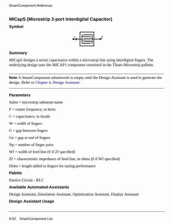
SmartComponent Reference
MICapS (Microstrip 2-port Interdigital Capacitor)
Symbol
Summary
MICapS designs a series capacitance within a microstrip line using interdigital fingers. Theunderlying design uses the MICAP1 component contained in the Tlines-Microstrip pallette.
Note A SmartComponent subnetwork is empty until the Design Assistant is used to generate thedesign. Refer to Chapter 4, Design Assistant.
Parameters
Subst = microstrip substrate name
F = center frequency, in hertz
C = capacitance, in farads
W = width of fingers
G = gap between fingers
Ge = gap at end of fingers
Np = number of finger pairs
Wf = width of feed line (0 if Zf specified)
Zf = characteristic impedance of feed line, in ohms (0 if Wf specified)
Delta = length added to fingers for tuning performance
Palette
Passive Circuit - RLC
Available Automated-Assistants
Design Assistant, Simulation Assistant, Optimization Assistant, Display Assistant
Design Assistant Usage
9-52 SmartComponent List

For general information, refer to Chapter 4, Design Assistant.
1. The design is accomplished using a simple model that specifies the length required toachieve the capacitance C at the design center frequency given the remaining physicalparameters. If the computed length is unreasonable, decreasing or increasing the gap G willincrease or decrease the capacitance, respectively and therefore allow altering of the length.
2. Both Wf and Zf specify the properties of the feed line. For proper operation, make sure thatonly one of these parameters is non-zero.
3. For more detailed discussion of the parameters W, G, Ge, Np, Wt, and Wf, please refer tothe discussion of MICAP1 in the Microstrip Components documentation.
Simulation Assistant Usage
For general information, refer to Chapter 5, Simulation Assistant.
Optimization Assistant Usage
For general information, refer to Chapter 6, Optimization Assistant.
The Optimization Assistant tunes the length of the fingers to achieve the desired capacitance.Because of the simple design approach used, it is often wise to first roughly tune the design withinthe Simulation Assistant and subsequently use the optimizer to perform the fine tuning.
Display Assistant Usage
For general information, refer to Chapter 7, Display Assistant.
Example
A MICapS component was used to design a 1 pF series capacitance for a 50 ohm line at a centerfrequency of 5 GHz. Optimization yielded a value of Delta = 2.443 mil.
SmartComponent List 9-53
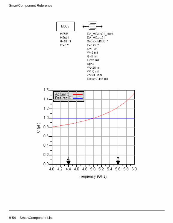
SmartComponent Reference
9-54 SmartComponent List

MICapSG (Microstrip 1-port Interdigital Capacitor)
Symbol
Summary
MICapSG designs a series capacitance between a microstrip line and ground using interdigitalfingers. The underlying design uses the MICAP3 component contained in the Tlines-Microstrippallette.
Note A SmartComponent subnetwork is empty until the Design Assistant is used to generate thedesign. Refer to Chapter 4, Design Assistant.
Parameters
Subst = microstrip substrate name
F = center frequency, in hertz
C = capacitance, in farads
W = width of fingers
G = gap between fingers
Ge = gap at end of fingers
Np = number of finger pairs
Wt = width of interconnect
Wf = width of feed line (0 if Zf specified)
Zf = characteristic impedance of feed line, in ohms (0 if Wf specified)
Delta = length added to fingers for tuning performance
Palette
Passive Circuit - RLC
Available Automated-Assistants
Design Assistant, Simulation Assistant, Optimization Assistant, Display Assistant
SmartComponent List 9-55
SmartComponent Reference
Design Assistant Usage
For general information, refer to Chapter 4, Design Assistant.
1. The design is accomplished using a simple model that specifies the length required toachieve the capacitance C at the design center frequency given the remaining physicalparameters. If the computed length is unreasonable, decreasing or increasing the gap G willincrease or decrease the capacitance, respectively and therefore allow altering of the length.
2. Both Wf and Zf specify the properties of the feed line. For proper operation, make sure thatonly one of these parameters is non-zero.
3. For more detailed discussion of the parameters W, G, Ge, Np, Wt, and Wf, please refer tothe discussion of MICAP3 in the Microstrip Components documentation.
Simulation Assistant Usage
For general information, refer to Chapter 5, Simulation Assistant.
Optimization Assistant Usage
For general information, refer to Chapter 6, Optimization Assistant.
The Optimization Assistant tunes the length of the fingers to achieve the desired capacitance.Because of the simple design approach used, it is often wise to first roughly tune the design withinthe Simulation Assistant and subsequently use the optimizer to perform the fine tuning.
Display Assistant Usage
For general information, refer to Chapter 7, Display Assistant.
Example
A MICapSG component was used to design a 1 pF capacitance for a 50 ohm line at a centerfrequency of 5 GHz. Optimization yielded a value of Delta = -1.841 mil.
9-56 SmartComponent List

SmartComponent List 9-57
SmartComponent Reference
MLine (Microstrip Line)
Symbol
Summary
MLine designs a microstrip line given the substrate, desired characteristic impedance, and physicalor electrical length.
Note A SmartComponent subnetwork is empty until the Design Assistant is used to generate thedesign. Refer to Chapter 4, Design Assistant.
Parameters
Subst = microstrip substrate name
F = design frequency, in hertz
Zo = desired characteristic impedance, in ohms
Lphys = physical line length (set to zero if Lelec specified)
Lelec = line length in wavelengths (set to zero if Lphys specified)
Palette
Passive Circuit - Lines
Available Automated-Assistants
Design Assistant
Design Assistant Usage
For general information, refer to Chapter 4, Design Assistant.
1. Since the design uses the models inherent to ADS to compute the line width and length,there is no need for a dedicated Simulation Assistant, Optimization Assistant, or DisplayAssistant.
2. For proper operation, either Lphys or Lelec must be zero.
9-58 SmartComponent List

3. Refer to the discussion of the MLIN component in the Microstrip Componentsdocumentation for a more detailed description of the model used for this component.
SmartComponent List 9-59

SmartComponent Reference
MMndr (Microstrip Meander Line)
Symbol
Summary
MMndr designs a meandering microstrip line given the substrate, desired characteristicimpedance, physical or electrical length, and maximum rectangular dimensions of the line.
Note A SmartComponent subnetwork is empty until the Design Assistant is used to generate thedesign. Refer to Chapter 4, Design Assistant.
Parameters
Subst = microstrip substrate name
F = design frequency, in hertz
Zo = desired characteristic impedance, in ohms
Lphys = physical line length (set to zero if Lelec specified)
Lelec = line length in wavelengths (set to zero if Lphys specified)
WR = bounding rectangle width, in meters
HR = bounding rectangle height, in meters
Delta = length added to vertical lines for tuning performance
Palette
Passive Circuit - Lines
Available Automated-Assistants
Design Assistant, Simulation Assistant, Optimization Assistant, Display Assistant
Design Assistant Usage
For general information, refer Chapter 4, Design Assistant.
1. The line input and output ports will be at the center of the rectangle on the side characterizedby HR.
9-60 SmartComponent List
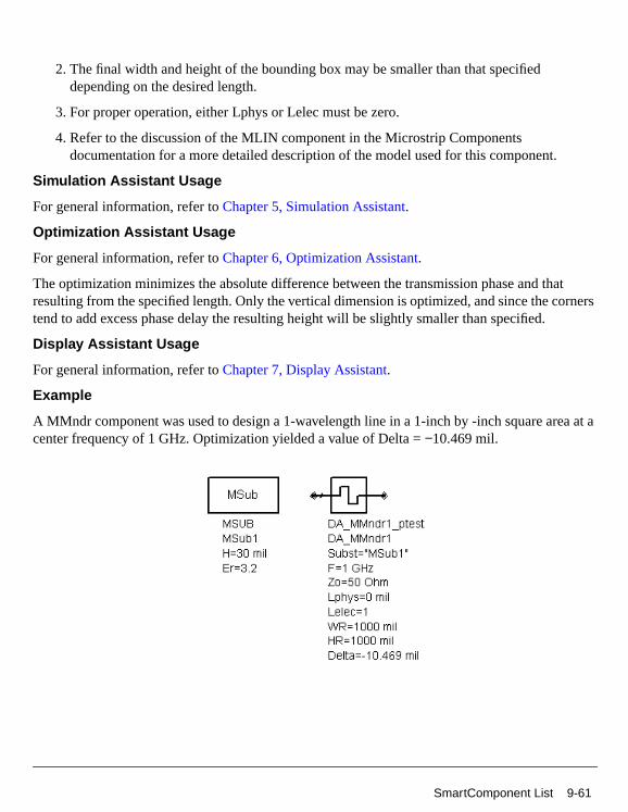
2. The final width and height of the bounding box may be smaller than that specifieddepending on the desired length.
3. For proper operation, either Lphys or Lelec must be zero.
4. Refer to the discussion of the MLIN component in the Microstrip Componentsdocumentation for a more detailed description of the model used for this component.
Simulation Assistant Usage
For general information, refer to Chapter 5, Simulation Assistant.
Optimization Assistant Usage
For general information, refer to Chapter 6, Optimization Assistant.
The optimization minimizes the absolute difference between the transmission phase and thatresulting from the specified length. Only the vertical dimension is optimized, and since the cornerstend to add excess phase delay the resulting height will be slightly smaller than specified.
Display Assistant Usage
For general information, refer to Chapter 7, Display Assistant.
Example
A MMndr component was used to design a 1-wavelength line in a 1-inch by -inch square area at acenter frequency of 1 GHz. Optimization yielded a value of Delta = −10.469 mil.
SmartComponent List 9-61
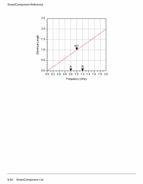
SmartComponent Reference
9-62 SmartComponent List
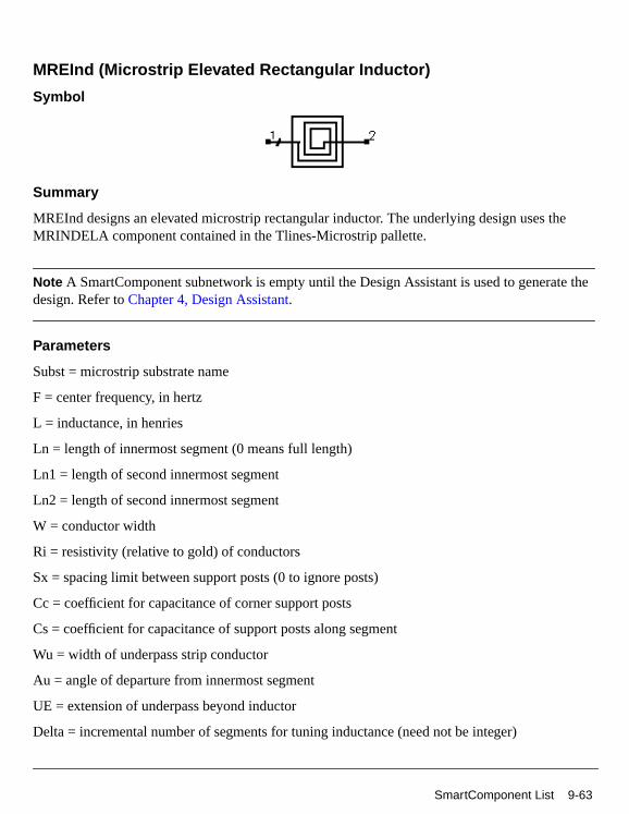
MREInd (Microstrip Elevated Rectangular Inductor)
Symbol
Summary
MREInd designs an elevated microstrip rectangular inductor. The underlying design uses theMRINDELA component contained in the Tlines-Microstrip pallette.
Note A SmartComponent subnetwork is empty until the Design Assistant is used to generate thedesign. Refer to Chapter 4, Design Assistant.
Parameters
Subst = microstrip substrate name
F = center frequency, in hertz
L = inductance, in henries
Ln = length of innermost segment (0 means full length)
Ln1 = length of second innermost segment
Ln2 = length of second innermost segment
W = conductor width
Ri = resistivity (relative to gold) of conductors
Sx = spacing limit between support posts (0 to ignore posts)
Cc = coefficient for capacitance of corner support posts
Cs = coefficient for capacitance of support posts along segment
Wu = width of underpass strip conductor
Au = angle of departure from innermost segment
UE = extension of underpass beyond inductor
Delta = incremental number of segments for tuning inductance (need not be integer)
SmartComponent List 9-63
SmartComponent Reference
Palette
Passive Circuit - RLC
Available Automated-Assistants
Design Assistant, Simulation Assistant, Display Assistant
Design Assistant Usage
For general information, refer to Chapter 4, Design Assistant.
1. The design is accomplished using a simple model that specifies the number of segments inthe rectangular inductor required to achieve the inductance L at the design center frequencygiven the remaining physical parameters.
2. The parameters from Hi through Cs are not actually used in the design process, andtherefore final tuning is required to achieve the proper value of the inductance.
3. The tuning parameter Delta represents the number of additional segments to add to theoutside of the structure. If it is not an integer value, the outermost segment (L1) will not befull length, with the fractional remainder of Delta specifying the fractional length of thisoutermost segment.
4. The values Ln, Ln1, and Ln2 represent the lengths Ln, Ln-1, and Ln-2 associated with theMRINDELA component. For more detailed discussion of these lengths as well as theparameters from W through UE, please refer to the discussion of MRINDELA in theMicrostrip Components documentation.
Simulation Assistant Usage
For general information, refer to Chapter 5, Simulation Assistant.
Optimization Assistant Usage
Because of the difficulties associated with tuning the inductor using additional discrete segments,no Optimization Assistant is provided. However, tuning can be accomplished quite effectively bymanually updating the value of Delta from within the Simulation Assistant. refer to Chapter 5,Simulation Assistant, as well as the following example for more details.
Display Assistant Usage
For general information, refer to Chapter 7, Display Assistant.
Example
A MREInd component was used to design a 1 nH inductor at a center frequency of 3 GHz. Thedesign used a full-length innermost segment. By tuning the number of segments within the
9-64 SmartComponent List
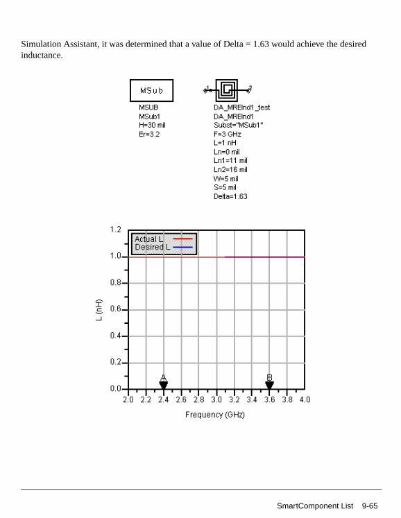
Simulation Assistant, it was determined that a value of Delta = 1.63 would achieve the desiredinductance.
SmartComponent List 9-65

SmartComponent Reference
MRInd (Microstrip Rectangular Inductor)
Symbol
Summary
MRInd designs a microstrip rectangular inductor. The underlying design uses the MRINDNBRand MRINDWBR components contained in the Tlines-Microstrip pallette.
Note A SmartComponent subnetwork is empty until the Design Assistant is used to generate thedesign. Refer to Chapter 4, Design Assistant.
Parameters
Subst = microstrip substrate name
F = center frequency, in hertz
L = inductance, in henries
IndType = inductance type (no bridge or wire bridge)
Ln = length of innermost segment (0 means full length)
Ln1 = length of second innermost segment
Ln2 = length of second innermost segment
W = conductor width
S = conductor spacing
Rb = resistivity (relative to gold) of bridge wire (for wire bridge)
Hw = height of wire above inductor (for wire bridge)
Aw = angle of departure from innermost segment (for wire bridge)
WE = extension of bridge beyond inductor (for wire bridge)
Delta = incremental number of segments for tuning inductance (need not be integer)
Palette
9-66 SmartComponent List
Passive Circuit - RLC
Available Automated-Assistants
Design Assistant, Simulation Assistant, Display Assistant
Design Assistant Usage
For general information, refer to Chapter 4, Design Assistant.
1. The design is accomplished using a simple model that specifies the number of segments inthe rectangular inductor required to achieve the inductance L at the design center frequencygiven the remaining physical parameters.
2. The parameters Rb and Hw are not actually used in the design process, and therefore finaltuning is required to achieve the proper value of the inductance.
3. The value of IndType specifies the type of inductor that will be designed. If this parameter isset to “No Bridge”, then the MRINDNBR component is designed and the parameters fromDw to WE are ignored. If the parameter is set to “Wire Bridge”, then the MRINDWBRcomponent is designed and the parameters from Dw to WE are used.
4. The tuning parameter Delta represents the number of additional segments to add to theoutside of the structure. If it is not an integer value, the outermost segment (L1) will not befull length, with the fractional remainder of Delta specifying the fractional length of thisoutermost segment.
5. The values Ln, Ln1, and Ln2 represent the lengths Ln, Ln-1, and Ln-2 associated with theMRINDNBR and MRINDWBR components. For more detailed discussion of these lengthsas well as the parameters W through WE, please refer to the discussion of these componentsin the Microstrip Components documentation.
Simulation Assistant Usage
For general information, refer to Chapter 5, Simulation Assistant.
Optimization Assistant Usage
Because of the difficulties associated with tuning the inductor using additional discrete segments,no Optimization Assistant is provided. However, tuning can be accomplished quite effectively bymanually updating the value of Delta from within the Simulation Assistant, refer to Chapter 5,Simulation Assistant, as well as the following example for more details.
Display Assistant Usage
For general information, refer to Chapter 7, Display Assistant.
Example
SmartComponent List 9-67

SmartComponent Reference
A MRInd component with no bridge was used to design a 1 nH inductor at a center frequency of 3GHz. The design used a full-length innermost segment. By tuning the number of segments withinthe Simulation Assistant, it was determined that a value of Delta = 0.52 would achieve the desiredinductance.
9-68 SmartComponent List

MRStub (Microstrip Radial Stub)
Symbol
Summary
MRStub designs a microstrip radial stub given the substrate, desired input reactance, and stubdimensions.
Note A SmartComponent subnetwork is empty until the Design Assistant is used to generate thedesign. Refer to Chapter 4, Design Assistant.
Parameters
Subst = microstrip substrate name
F = design frequency, in hertz
Xin = desired input reactance, in ohms (only one of Xin, Cin, and Lin can be non-zero)
Cin = desired input capacitance, in farads (only one of Xin, Cin, and Lin can be non-zero)
Lin = desired input inductance, in henries (only one of Xin, Cin, and Lin can be non-zero)
W = width of feed line (set to zero if Z specified)
Z = characteristic impedance of feed line (set to zero if W specified)
Angle = subtended angle of circular sector
Delta = length added to stub for tuning performance
Palette
Passive Circuit - Lines
Available Automated-Assistants
Design Assistant, Simulation Assistant, Optimization Assistant, Display Assistant
Design Assistant Usage
For general information, refer to Chapter 4, Design Assistant.
SmartComponent List 9-69

SmartComponent Reference
1. The stub is designed by dividing the radial line into several short segments.
2. For proper operation, only one of Xin, Cin, and Lin can be non-zero. If all are zero, the stubis designed to provide an open circuit.
3. Refer to the discussion of the MRSTUB component in the Microstrip Componentsdocumentation for a more detailed description of the model used for this component.
Simulation Assistant Usage
For general information, refer to Chapter 5, Simulation Assistant.
Optimization Assistant Usage
For general information, refer to Chapter 6, Optimization Assistant.
The optimization changes the length of the stubs to achieve the desired input reactance.
Display Assistant Usage
For general information, refer to Chapter 7, Display Assistant.
Example
A MRStub component was used to design an open circuit stub at a center frequency of 1 GHz.Optimization yielded a value of Delta = -40.092 mil.
9-70 SmartComponent List

SmartComponent List 9-71
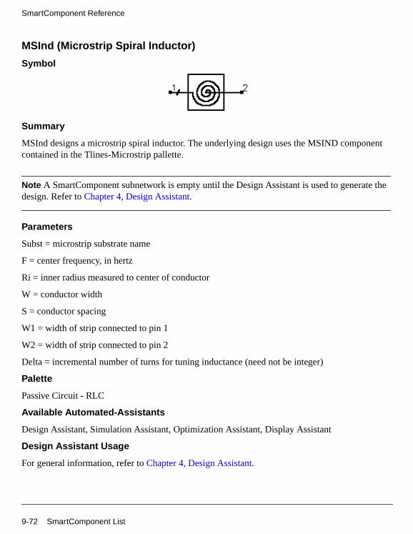
SmartComponent Reference
MSInd (Microstrip Spiral Inductor)
Symbol
Summary
MSInd designs a microstrip spiral inductor. The underlying design uses the MSIND componentcontained in the Tlines-Microstrip pallette.
Note A SmartComponent subnetwork is empty until the Design Assistant is used to generate thedesign. Refer to Chapter 4, Design Assistant.
Parameters
Subst = microstrip substrate name
F = center frequency, in hertz
Ri = inner radius measured to center of conductor
W = conductor width
S = conductor spacing
W1 = width of strip connected to pin 1
W2 = width of strip connected to pin 2
Delta = incremental number of turns for tuning inductance (need not be integer)
Palette
Passive Circuit - RLC
Available Automated-Assistants
Design Assistant, Simulation Assistant, Optimization Assistant, Display Assistant
Design Assistant Usage
For general information, refer to Chapter 4, Design Assistant.
9-72 SmartComponent List
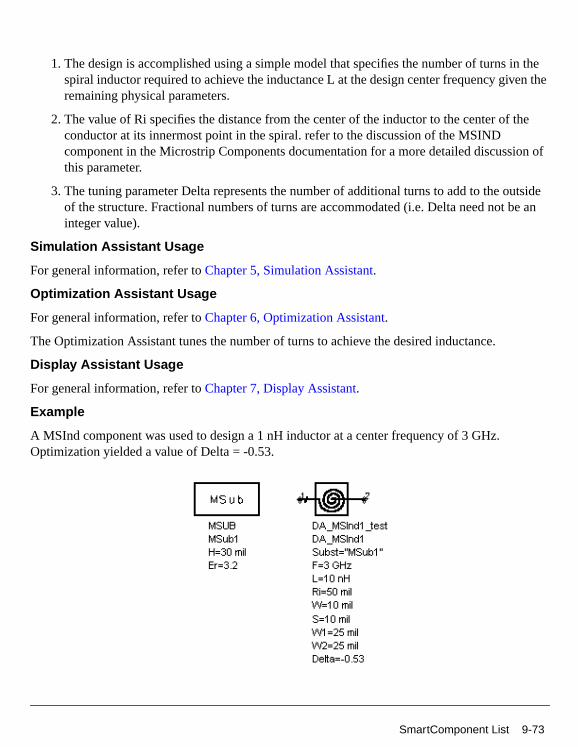
1. The design is accomplished using a simple model that specifies the number of turns in thespiral inductor required to achieve the inductance L at the design center frequency given theremaining physical parameters.
2. The value of Ri specifies the distance from the center of the inductor to the center of theconductor at its innermost point in the spiral. refer to the discussion of the MSINDcomponent in the Microstrip Components documentation for a more detailed discussion ofthis parameter.
3. The tuning parameter Delta represents the number of additional turns to add to the outsideof the structure. Fractional numbers of turns are accommodated (i.e. Delta need not be aninteger value).
Simulation Assistant Usage
For general information, refer to Chapter 5, Simulation Assistant.
Optimization Assistant Usage
For general information, refer to Chapter 6, Optimization Assistant.
The Optimization Assistant tunes the number of turns to achieve the desired inductance.
Display Assistant Usage
For general information, refer to Chapter 7, Display Assistant.
Example
A MSInd component was used to design a 1 nH inductor at a center frequency of 3 GHz.Optimization yielded a value of Delta = -0.53.
SmartComponent List 9-73
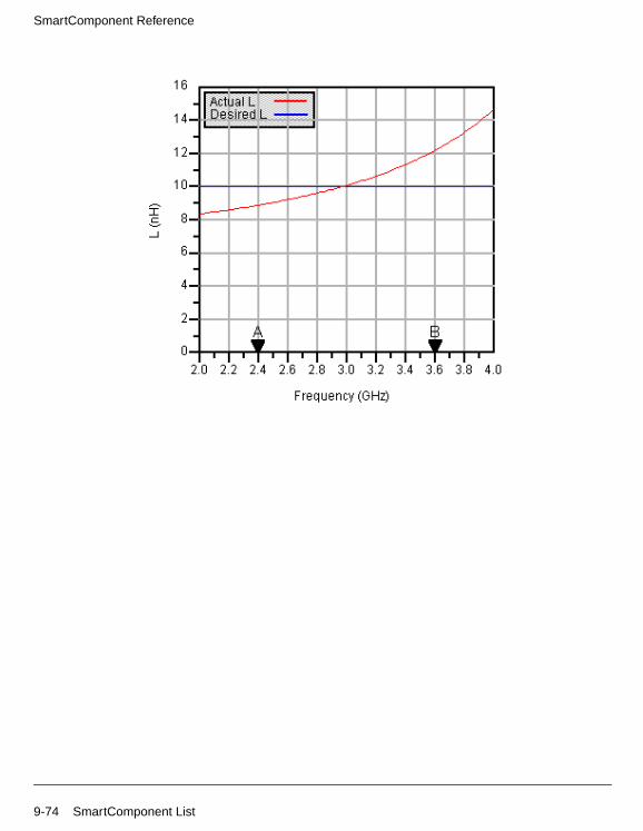
SmartComponent Reference
9-74 SmartComponent List

MStep (Microstrip Step Component)
Symbol
Summary
MStep designs a microstrip step given the substrate and desired characteristic impedances.
Note A SmartComponent subnetwork is empty until the Design Assistant is used to generate thedesign. Refer to Chapter 4, Design Assistant.
Parameters
Subst = microstrip substrate name
F = design frequency, in hertz
Z1 = characteristic impedance of port 1, in ohms
Z2 = characteristic impedance of port 2, in ohms
Palette
Passive Circuit - Lines
Available Automated-Assistants
Design Assistant
Design Assistant Usage
For general information, refer to Chapter 4, Design Assistant.
1. Since the design uses the models inherent to ADS to compute the line width, there is noneed for a dedicated Simulation Assistant, Optimization Assistant, or Display Assistant.
2. Refer to the discussion of the MSTEP component in the Microstrip Componentsdocumentation for a detailed description of this component.
SmartComponent List 9-75

SmartComponent Reference
MStub (Microstrip Stub)
Symbol
Summary
MStub designs a microstrip open or short circuited stub given the substrate, desired characteristicimpedance, and physical or electrical length. The design will realize the native MLOC, MLSC,and MLEF components.
Note A SmartComponent subnetwork is empty until the Design Assistant is used to generate thedesign. Refer to Chapter 4, Design Assistant.
Parameters
Subst = microstrip substrate name
F = design frequency, in hertz
Zo = desired characteristic impedance, in ohms
Lphys = physical line length
Lelec = line length in wavelengths
Xin = desired input reactance, in ohms
Cin = desired input capacitance, in farads
Lin = desired input inductance, in henries
StubType = type of stub
Only one of Lphys, Lelec, Xin, Cin, and Lin can be non-zero.
Palette
Passive Circuit - Lines
Available Automated-Assistants
Design Assistant
Design Assistant Usage
9-76 SmartComponent List

For general information, refer to Chapter 4, Design Assistant.
1. Since the design uses the models inherent to ADS to compute the line width and length,there is no need for a dedicated Simulation Assistant, Optimization Assistant, or DisplayAssistant.
2. For proper operation, only one of Lphys, Lelec, Xin, Cin, and Lin can be non-zero.
3. StubType can be either Open Circuit (MLOC), End Effect (MLEF), or Short Circuit(MLSC). Refer to the discussion of these components in the Microstrip Componentsdocumentation for a more detailed description of these different options.
SmartComponent List 9-77
SmartComponent Reference
MTaper (Microstrip Taper Component)
Symbol
Summary
MTaper designs a microstrip tapered line given the substrate, desired characteristic impedance,and physical or electrical length.
Note A SmartComponent subnetwork is empty until the Design Assistant is used to generate thedesign. Refer to Chapter 4, Design Assistant.
Parameters
Subst = microstrip substrate name
F = design frequency, in hertz
Z1 = characteristic impedance at port 1, in ohms
Z2 = characteristic impedance at port 2, in ohms
Lphys = physical line length (set to zero if Lelec specified)
Lelec = line length in wavelengths (set to zero if Lphys specified)
Palette
Passive Circuit - Lines
Available Automated-Assistants
Design Assistant
Design Assistant Usage
For general information, refer to Chapter 4, Design Assistant.
1. Since the design uses the models inherent to ADS to compute the line width and length,there is no need for a dedicated Simulation Assistant, Optimization Assistant, or DisplayAssistant.
2. For proper operation, either Lphys or Lelec must be zero.
9-78 SmartComponent List

3. Z1 and Z2 are used to determine the widths at each end of the taper component. Refer to thediscussion of the MTAPER component in the Microstrip Components documentation for amore detailed description of this component.
SmartComponent List 9-79

SmartComponent Reference
MTee (Microstrip Tee Component)
Symbol
Summary
MTee designs a microstrip tee given the substrate and desired characteristic impedance at eachport.
Note A SmartComponent subnetwork is empty until the Design Assistant is used to generate thedesign. Refer to Chapter 4, Design Assistant.
Parameters
Subst = microstrip substrate name
F = design frequency, in hertz
Z1 = characteristic impedance of port 1, in ohms
Z2 = characteristic impedance of port 2, in ohms
Z3 = characteristic impedance of port 3, in ohms
Palette
Passive Circuit - Lines
Available Automated-Assistants
Design Assistant
Design Assistant Usage
For general information, refer to Chapter 4, Design Assistant.
1. Since the design uses the models inherent to ADS to compute the line width and length,there is no need for a dedicated Simulation Assistant, Optimization Assistant, or DisplayAssistant.
9-80 SmartComponent List

2. Z1, Z2, and Z3 are used to determine the widths of each port. Refer to the discussion of theMTEE component in the Microstrip Components documentation for a more detaileddescription of this component.
SmartComponent List 9-81

SmartComponent Reference
MTFC (Microstrip Thin Film Capacitor)
Symbol
Summary
MTFC designs a microstrip thin film capacitor. The underlying design uses the MTFC componentcontained in the Tlines-Microstrip pallette.
Note A SmartComponent subnetwork is empty until the Design Assistant is used to generate thedesign. Refer to Chapter 4, Design Assistant.
Parameters
Subst = microstrip substrate name
F = center frequency, in hertz
C = capacitance, in farads
W = conductor width (set to 0 if Zo specified)
Zo = characteristic impedance of line for computing W (set to 0 if W specified)
CPUA = capacitance per unit area, in pf/mm^2
T = thickness of capacitor dielectric
RsT = sheet resistance of top metal plate, in ohms
RsB = sheet resistance of bottom metal plate, in ohms
TT = thickness of top metal plate
TB = thickness of bottom metal plate
COB= bottom conductor overlap
COT = top conductor overlap
DO = dielectric overlap
Delta = length added to conductor for tuning capacitance
9-82 SmartComponent List

Palette
Passive Circuit - RLC
Available Automated-Assistants
Design Assistant, Simulation Assistant, Optimization Assistant, Display Assistant
Design Assistant Usage
For general information, refer to Chapter 4, Design Assistant.
1. The design is accomplished by determining the length required to achieve the desiredcapacitance using the capacitance per unit area (CPUA) in conjunction with the specifiedwidth (W).
2. Since this capacitor is often fed with a microstrip line, either the physical width or thecharacteristic impedance of a microstrip line on the substrate can be specified. However,only one of the parameters should be non-zero.
3. The parameters from RsT through DO inclusive are not used in the design process but arepassed on to the underlying MTFC component and therefore included in any simulations oroptimizations.
4. The tuning parameter Delta represents incremental length required to achieve the desiredcapacitance. It is typically relatively small, as the initial design tends to be accurate.
Simulation Assistant Usage
For general information, refer to Chapter 5, Simulation Assistant.
Optimization Assistant Usage
For general information, refer to Chapter 6, Optimization Assistant.
The Optimization Assistant tunes the conductor length to achieve the desired capacitance.
Display Assistant Usage
For general information, refer to Chapter 7, Display Assistant.
Example
A MTFC component was used to design a 100 pF capacitor at a center frequency of 2 GHz. Theconductor width corresponds to that of a 50 ohm microstrip line fabricated on MSub1.Optimization yielded a value of Delta = -2.411.
SmartComponent List 9-83
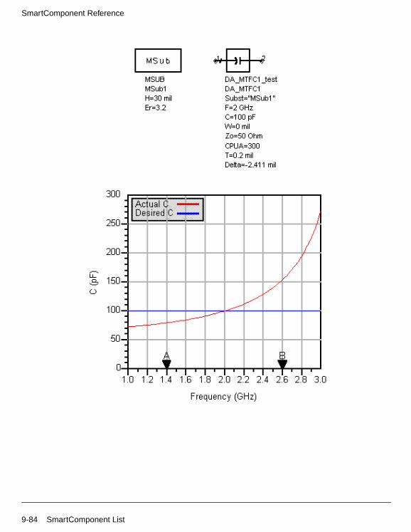
SmartComponent Reference
9-84 SmartComponent List
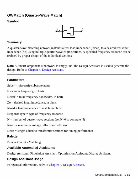
QWMatch (Quarter-Wave Match)
Symbol
Summary
A quarter-wave matching network matches a real load impedance (Rload) to a desired real inputimpedance (Zo) using multiple quarter wavelength sections. A specified frequency response can berealized by proper design of the individual sections.
Note A SmartComponent subnetwork is empty until the Design Assistant is used to generate thedesign. Refer to Chapter 4, Design Assistant.
Parameters
Subst = microstrip substrate name
F = center frequency, in hertz
DeltaF = total frequency bandwidth, in hertz
Zo = desired input impedance, in ohms
Rload = load impedance to match, in ohms
ResponseType = type of frequency response
N = number of quarter-wave sections (set N=0 to compute N)
Rmax = maximum voltage reflection coefficient
Delta = length added to transformer sections for tuning performance
Palette
Passive Circuit - Matching
Available Automated-Assistants
Design Assistant, Simulation Assistant, Optimization Assistant, Display Assistant
Design Assistant Usage
For general information, refer to Chapter 4, Design Assistant.
SmartComponent List 9-85

SmartComponent Reference
1. DeltaF is defined as the total bandwidth centered at the design center frequency.
2. If the number of sections N is set to zero, the Design Assistant chooses N such that thereflection coefficient is less that Rmax over the bandwidth DeltaF. The resulting bandwidthmay be broader than that specified. Otherwise, Rmax and DeltaF are ignored.
3. The ResponseType specifies the distribution of the partial reflection coefficients seen at eachsection interface - Uniform, Binomial, and Chebyshev distributions are available. These inturn specify the shape of the reflection coefficient versus frequency.
4. A single-section quarter-wave matching transformer can be designed by setting N = 1.
5. For a more detailed discussion of this device, see: D. M. Pozar, Microwave Engineering,2nd Edition, John Wiley & Sons: New York, 1998, pp. 275-288; R. S. Elliott, AnIntroduction to Guided Waves and Microwave Circuits, Prentice Hall, John Wiley, NewJersey, 1993, pp. 218-224.
Simulation Assistant Usage
For general information, refer to Chapter 5, Simulation Assistant.
Optimization Assistant Usage
For general information, refer to the Chapter 6, Optimization Assistant.
Since the reflection coefficient may not be at its minimum value at the design center frequency, theoptimization centers the variation of S11 (referenced to the value of Zo) versus frequency at thecenter frequency by changing the length of each quarter-wave section. All sections are tuned bythe same length during the optimization.
Display Assistant Usage
For general information, refer to Chapter 7, Display Assistant.
Example
A quarter-wave matching network was designed to match a load impedance of 100 ohms to a 50ohm line at a center frequency of 4 GHz. Specifying a Chebyshev frequency response for whichthe reflection coefficient remains below 0.1 over a 3 GHz bandwidth dictates 3 quarter-wavesections. Tuning using the Optimization Assistant yielded a value of Delta =-2.284 mil.
9-86 SmartComponent List
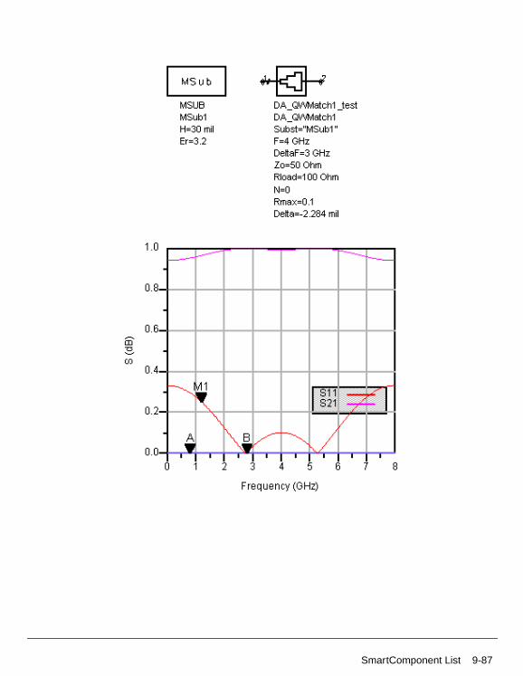
SmartComponent List 9-87
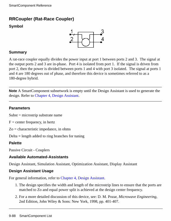
SmartComponent Reference
RRCoupler (Rat-Race Coupler)
Symbol
Summary
A rat-race coupler equally divides the power input at port 1 between ports 2 and 3. The signal atthe output ports 2 and 3 are in-phase. Port 4 is isolated from port 1. If the signal is driven fromport 2, then the power is divided between ports 1 and 4 with port 3 isolated. The signal at ports 1and 4 are 180 degrees out of phase, and therefore this device is sometimes referred to as a180-degree hybrid.
Note A SmartComponent subnetwork is empty until the Design Assistant is used to generate thedesign. Refer to Chapter 4, Design Assistant.
Parameters
Subst = microstrip substrate name
F = center frequency, in hertz
Zo = characteristic impedance, in ohms
Delta = length added to ring branches for tuning
Palette
Passive Circuit - Couplers
Available Automated-Assistants
Design Assistant, Simulation Assistant, Optimization Assistant, Display Assistant
Design Assistant Usage
For general information, refer to Chapter 4, Design Assistant.
1. The design specifies the width and length of the microstrip lines to ensure that the ports arematched to Zo and equal power split is achieved at the design center frequency.
2. For a more detailed discussion of this device, see: D. M. Pozar, Microwave Engineering,2nd Edition, John Wiley & Sons: New York, 1998, pp. 401-407.
9-88 SmartComponent List
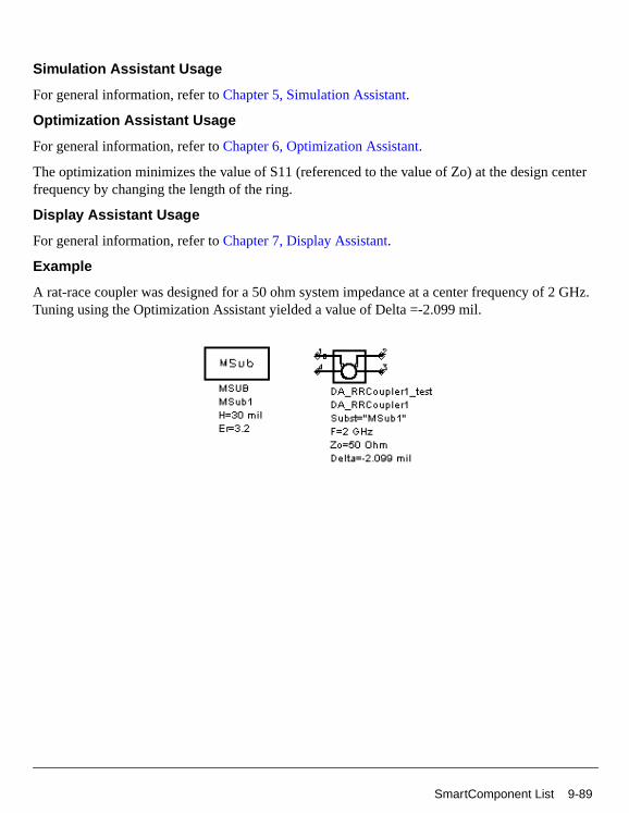
Simulation Assistant Usage
For general information, refer to Chapter 5, Simulation Assistant.
Optimization Assistant Usage
For general information, refer to Chapter 6, Optimization Assistant.
The optimization minimizes the value of S11 (referenced to the value of Zo) at the design centerfrequency by changing the length of the ring.
Display Assistant Usage
For general information, refer to Chapter 7, Display Assistant.
Example
A rat-race coupler was designed for a 50 ohm system impedance at a center frequency of 2 GHz.Tuning using the Optimization Assistant yielded a value of Delta =-2.099 mil.
SmartComponent List 9-89
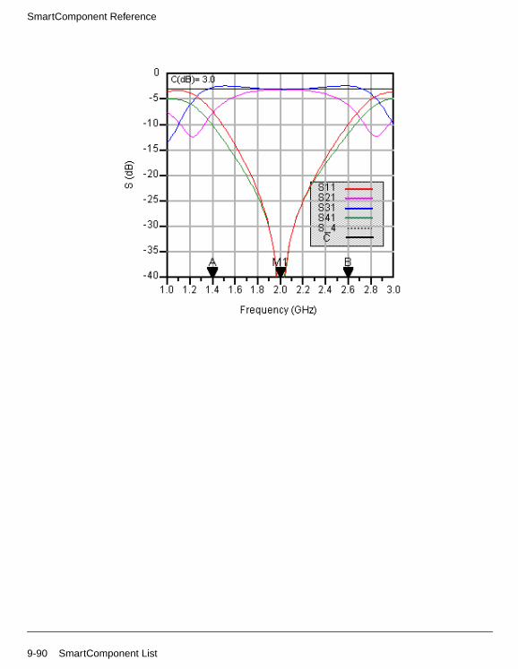
SmartComponent Reference
9-90 SmartComponent List

SBFilter (Stub Bandpass Filter)
Symbol
Summary
A stub bandpass filter provides a bandpass frequency response between the input and output ports.The design uses shunt stubs connected by lengths of transmission line. If the specified passbandresponse is too narrow, large differences in impedance values may result in a non-realizableconfiguration.
Note A SmartComponent subnetwork is empty until the Design Assistant is used to generate thedesign. Refer to Chapter 4, Design Assistant.
Parameters
Subst = microstrip substrate name
Fs1 = lower stopband edge frequency, in hertz
Fp1 = lower passband edge frequency, in hertz
Fp2 = upper passband edge frequency, in hertz
Fs2 = lower stopband edge frequency, in hertz
Ap = passband edge attenuation (or ripple for Chebyshev), in dB
As = stopband edge attenuation, in dB
N = number of filter sections (or 0 to compute N)
ResponseType = type of frequency response (maximally flat or Chebyshev)
StubConfig = configuration of interior shunt stubs
Zo = desired input/output impedance, in ohms
D = impedance control parameter (0 < D < 1)
Delta = length added to stubs for tuning performance
Palette
SmartComponent List 9-91

SmartComponent Reference
Passive Circuit - Filters
Available Automated-Assistants
Design Assistant, Simulation Assistant, Optimization Assistant, Display Assistant
Design Assistant Usage
For general information, refer to Chapter 4, Design Assistant.
1. This design is typically practical for fractional bandwidths of 0.4 to 0.7 or higher. If thebandwidth is too narrow, the design will generally require large differences in impedancesbetween the stubs and the connecting lines, producing an unrealizable configuration.
2. For a Chebyshev (equal ripple) frequency response, ripple levels greater than about 1 dB arenot recommended. Exceeding this value will typically deform the shape of the passbandcharacteristics.
3. The parameter StubConfig specifies whether the interior stubs (all but those closest to thesource and load) are implemented as a single stub or as two stubs in parallel. Choosing asingle stub often produces narrower stub linewidths, and therefore this parameter can impactthe ability to manufacture.
4. The parameter D offers some control over the ratio between the stub impedances at the endsof the filter to those in the interior. In some cases where a MCROSS or MTEE widthconstraint violation is encountered, decreasing (or increasing) this value in the range 0 < D< 1 may remedy the problem.
5. If N is zero, the number of filter sections will be computed from the frequency/attenuationinformation. If N is non-zero, the design will use the frequency/attenuation parameters onlyfor determining the design center frequency.
6. For a more detailed discussion of this device, see: Matthaei, Young and Jones, MicrowaveFilters, Impedance-Matching Networks, and Coupling Structures, Artech House, 1980, pp.595-608.
Simulation Assistant Usage
For general information, refer to Chapter 5, Simulation Assistant.
Optimization Assistant Usage
For general information, refer to Chapter 6, Optimization Assistant.
The optimization minimizes the absolute difference between S21 and the specified passband edgeattenuation (which equals the ripple for Chebyshev response) at the passband edge frequencies.All stub lengths are tuned by the same amount. Because only the stub lengths are changed, this
9-92 SmartComponent List

tuning will typically center the response within the specified passband. More advanced shaping ofthe passband response can be accomplished by manually tuning the widths and lengths of all lines.
Display Assistant Usage
For general information, refer to Chapter 7, Display Assistant.
Example
A stub bandpass filter was designed for a Chebyshev response with a 0.1 dB ripple. The passbandedge frequencies are at 1.3GHz and 2.7 GHz respectively. The design uses two parallel stubs in theinterior regions with D = 1. The design required 4 stubs. Tuning using the Optimization Assistantyielded a value of Delta = -19.316 mil.
SmartComponent List 9-93

SmartComponent Reference
9-94 SmartComponent List

SIFilter (Stepped Impedance Lowpass Filter)
Symbol
Summary
A stepped impedance filter provides a lowpass frequency response between the input and outputports. The design is realized using alternating wide and narrow microstrip lines.
Note A SmartComponent subnetwork is empty until the Design Assistant is used to generate thedesign. Refer to Chapter 4, Design Assistant.
Parameters
Subst = microstrip substrate name
Fp = frequency at passband edge, in hertz
Ap = passband edge attenuation (or ripple for Chebyshev), in dB
Fs = frequency at stopband edge, in hertz
As = stopband edge attenuation, in dB
N = number of filter sections (or 0 to compute N)
ResponseType = type of frequency response (maximally flat or Chebyshev)
FElement = first filter component (automatic, capacitive, or inductive)
Zo = desired input/output impedance, in ohms
ZL = characteristic impedance of low impedance sections, in ohms
ZH = characteristic impedance of high impedance sections, in ohms
Delta = length added to filter sections for tuning performance
Palette
Passive Circuit - Filters
Available Automated-Assistants
SmartComponent List 9-95
SmartComponent Reference
Design Assistant, Simulation Assistant, Optimization Assistant, Display Assistant
Design Assistant Usage
For general information, refer to Chapter 4, Design Assistant.
1. The stepped impedance filter uses wide microstrip lines to approximate shunt capacitors andnarrow lines to approximate series inductors in order to provide a lowpass frequencyresponse.
2. For a Chebyshev (equal ripple) frequency response, ripple levels greater than about 1 dB arenot recommended. Exceeding this value will typically deform the shape of the passbandcharacteristics. In order to obtain an impedance match, Chebyshev designs must use an oddnumber of components (N).
3. The parameter FElement specifies whether the first stub is inductive or capacitive. IfAutomatic is chosen, the first component is inductive if Zo/ZL > ZH/Zo and capacitiveotherwise.
4. If N is zero, the number of filter sections will be computed from the frequency/attenuationinformation. If N is non-zero, the design will use the frequency/attenuation parameters onlyfor determining the design center frequency.
5. Because this filter design strategy is approximate, the resulting stopband attenuation maynot satisfy the specification. Choosing more sections than that computed by the design canimprove the stopband performance.
6. For a more detailed discussion of this device, see: Matthaei, Young and Jones, MicrowaveFilters, Impedance-Matching Networks, and Coupling Structures, Artech House, 1980, pp.365-374.
Simulation Assistant Usage
For general information, refer to Chapter 5, Simulation Assistant.
Optimization Assistant Usage
For general information, refer to Chapter 6, Optimization Assistant.
The optimization minimizes the absolute difference between S21 and the specified passband edgeattenuation (which equals the ripple for Chebyshev response) at the passband edge frequency. Allfilter sections are tuned by the same amount.
Display Assistant Usage
For general information, refer to Chapter 7, Display Assistant.
Example
9-96 SmartComponent List

A stepped impedance lowpass filter was designed for a maximally flat response with a 3 dBattenuation at the passband edge frequency of 4 GHz. Choosing FElement as Automatic results ina capacitive first component. Tuning using the Optimization Assistant yielded a value of Delta =27.446 mil.
SmartComponent List 9-97
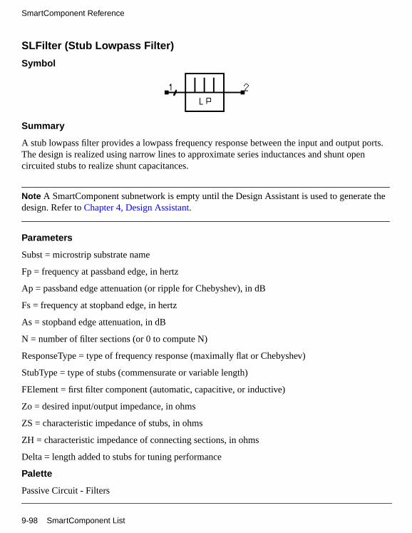
SmartComponent Reference
SLFilter (Stub Lowpass Filter)
Symbol
Summary
A stub lowpass filter provides a lowpass frequency response between the input and output ports.The design is realized using narrow lines to approximate series inductances and shunt opencircuited stubs to realize shunt capacitances.
Note A SmartComponent subnetwork is empty until the Design Assistant is used to generate thedesign. Refer to Chapter 4, Design Assistant.
Parameters
Subst = microstrip substrate name
Fp = frequency at passband edge, in hertz
Ap = passband edge attenuation (or ripple for Chebyshev), in dB
Fs = frequency at stopband edge, in hertz
As = stopband edge attenuation, in dB
N = number of filter sections (or 0 to compute N)
ResponseType = type of frequency response (maximally flat or Chebyshev)
StubType = type of stubs (commensurate or variable length)
FElement = first filter component (automatic, capacitive, or inductive)
Zo = desired input/output impedance, in ohms
ZS = characteristic impedance of stubs, in ohms
ZH = characteristic impedance of connecting sections, in ohms
Delta = length added to stubs for tuning performance
Palette
Passive Circuit - Filters
9-98 SmartComponent List
Available Automated-Assistants
Design Assistant, Simulation Assistant, Optimization Assistant, Display Assistant
Design Assistant Usage
For general information, refer to Chapter 4, Design Assistant.
1. The stub lowpass filter uses narrow microstrip lines that approximate series inductorsconnecting open-circuited stubs that approximate shunt capacitors in order to provide alowpass frequency response.
2. For a Chebyshev (equal ripple) frequency response, ripple levels greater than about 1 dB arenot recommended. Exceeding this value will typically deform the shape of the passbandcharacteristics. In order to obtain an impedance match, Chebyshev designs must use an oddnumber of components (N).
3. If the parameter StubType is set as Commensurate, all stubs will have equal lengths, and thestub line width is computed. The value of ZS is then ignored, and the resulting design maybe difficult to realize. If StubType is set as Variable Length Stub, the stub line widths aredetermined from ZS and the stub lengths are computed from the specifications.
4. The parameter FElement specifies whether the first stub is inductive or capacitive. IfAutomatic is chosen, the first component is set to be capacitive since this tends to offerimprovements in manufacturing.
5. If N is zero, the number of filter sections will be computed from the frequency/attenuationinformation. If N is non-zero, the design will use the frequency/attenuation parameters onlyfor determining the design center frequency. Because this filter design strategy isapproximate, the resulting stopband attenuation may not satisfy the specification. Choosingmore sections than that computed by the Design Assistant can improve the stopbandperformance.
6. For a more detailed discussion of this device, refer to: Matthaei, Young and Jones,Microwave Filters, Impedance-Matching Networks, and Coupling Structures, ArtechHouse, 1980, pp. 375.
Simulation Assistant Usage
For general information, refer to Chapter 5, Simulation Assistant.
Optimization Assistant Usage
For general information, refer to Chapter 6, Optimization Assistant.
SmartComponent List 9-99
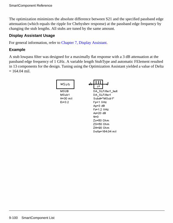
SmartComponent Reference
The optimization minimizes the absolute difference between S21 and the specified passband edgeattenuation (which equals the ripple for Chebyshev response) at the passband edge frequency bychanging the stub lengths. All stubs are tuned by the same amount.
Display Assistant Usage
For general information, refer to Chapter 7, Display Assistant.
Example
A stub lowpass filter was designed for a maximally flat response with a 3 dB attenuation at thepassband edge frequency of 1 GHz. A variable length StubType and automatic FElement resultedin 13 components for the design. Tuning using the Optimization Assistant yielded a value of Delta= 164.04 mil.
9-100 SmartComponent List
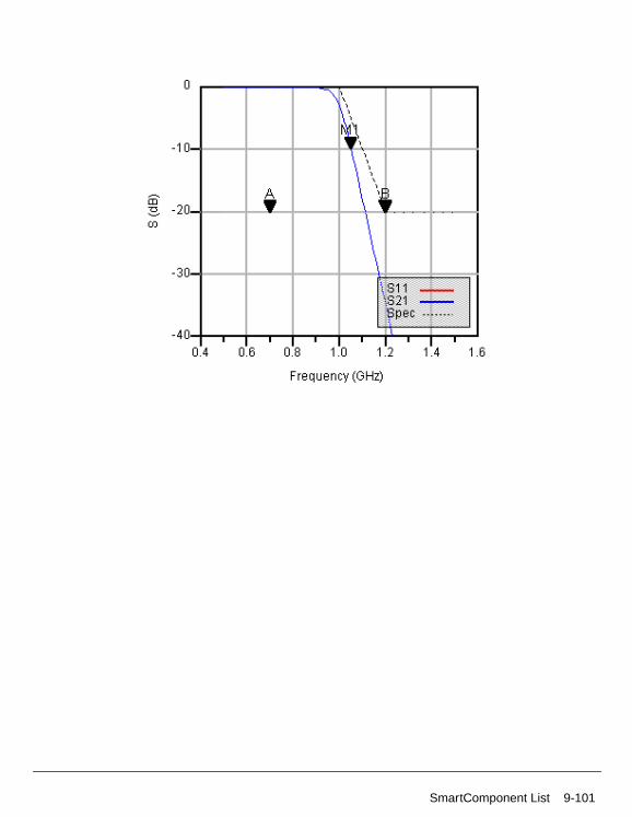
SmartComponent List 9-101

SmartComponent Reference
SRFilter (Stepped Impedance Resonator Filter)
Symbol
Summary
A stepped impedance resonator filter provides a bandpass frequency response between the inputand output ports. N coupled-line sections produce an N−1 order filter response. Additionalnumbers of sections can be used to steepen the transition band roll off or widen the passbandwidth. The use on non-uniform impedance for each resonator moves the second pass bandcenter frequency away from the second harmonic of the fundamental frequency.
Note A SmartComponent subnetwork is empty until the Design Assistant is used to generate thedesign. Refer to Chapter 4, Design Assistant.
Parameters
Subst = microstrip substrate name
Fs1 = lower stopband edge frequency, in hertz
Fp1 = lower passband edge frequency, in hertz
Fp2 = upper passband edge frequency, in hertz
Fs2 = lower stopband edge frequency, in hertz
Ap = passband edge attenuation (or ripple for Chebyshev), in dB
As = stopband edge attenuation, in dB
N = number of filter sections (or 0 to compute N)
ResponseType = type of frequency response (maximally flat or Chebyshev)
Zo = desired input/output impedance, in ohms
Fsp = center frequency of first spurious passband
Delta = length added to filter sections for tuning performance
Palette
9-102 SmartComponent List
Passive Circuit - Filters
Available Automated-Assistants
Design Assistant, Simulation Assistant, Optimization Assistant, Display Assistant
Design Assistant Usage
For general information, refer to Chapter 4, Design Assistant.
1. Because of the heavy computational burden in determining the line parameters, a brief delaywill occur for the design.
2. For a Chebyshev (equal ripple) frequency response, ripple levels greater than about 1 dB arenot recommended. Exceeding this value will typically deform the shape of the passbandcharacteristics.
3. If N is zero, the number of filter sections will be computed from the frequency/attenuationinformation. If N is non-zero, the design will use the frequency/attenuation parameters onlyfor determining the design center frequency.
4. The center frequency of the first spurious passband should be on the order of twice thefundamental passband center frequency.
5. For a more detailed discussion of this device, refer to: Makimoto and Yamashita, “Bandpassfilters using parallel coupled stripline stepped impedance resonators,” IEEE Trans.Microwave Theory and Techniques, vol MTT-28, pp. 1413-1417, 1980.
Simulation Assistant Usage
For general information, refer to Chapter 5, Simulation Assistant.
Optimization Assistant Usage
For general information, refer to Chapter 6, Optimization Assistant.
The optimization minimizes the absolute difference between S21 in dB and the specified passbandedge attenuation (which equals the ripple for Chebyshev response) at the passband edgefrequencies. Because only the line lengths are changed, this tuning will typically center theresponse within the specified passband. More advanced shaping of the passband response can beaccomplished by manually tuning the widths and spacings of the coupled filter sections.
Display Assistant Usage
For general information, refer to Chapter 7, Display Assistant.
Example
SmartComponent List 9-103

SmartComponent Reference
A stepped impedance resonator filter was designed for a maximally flat response with the 3 dBpassband edge frequencies at 2 GHz and 2.2 GHz respectively. The second passband was set to 4.1GHz. The design required 4 coupled lines. Tuning using the Optimization Assistant yielded avalue of Delta = 0.785 mil.
9-104 SmartComponent List
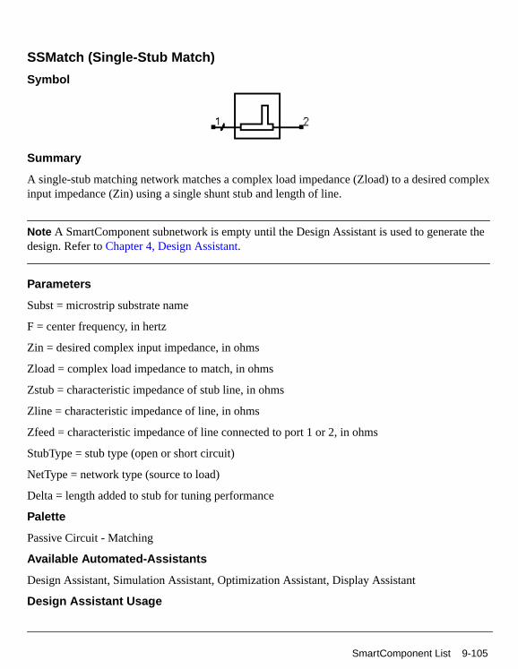
SSMatch (Single-Stub Match)
Symbol
Summary
A single-stub matching network matches a complex load impedance (Zload) to a desired complexinput impedance (Zin) using a single shunt stub and length of line.
Note A SmartComponent subnetwork is empty until the Design Assistant is used to generate thedesign. Refer to Chapter 4, Design Assistant.
Parameters
Subst = microstrip substrate name
F = center frequency, in hertz
Zin = desired complex input impedance, in ohms
Zload = complex load impedance to match, in ohms
Zstub = characteristic impedance of stub line, in ohms
Zline = characteristic impedance of line, in ohms
Zfeed = characteristic impedance of line connected to port 1 or 2, in ohms
StubType = stub type (open or short circuit)
NetType = network type (source to load)
Delta = length added to stub for tuning performance
Palette
Passive Circuit - Matching
Available Automated-Assistants
Design Assistant, Simulation Assistant, Optimization Assistant, Display Assistant
Design Assistant Usage
SmartComponent List 9-105
SmartComponent Reference
For general information, refer to Chapter 4, Design Assistant.
1. The parameter NetType can be Automatic, stub-line, or line-stub, with the latter two choicesrepresenting configurations that have a stub followed by a line or vice-versa as the networkis observed from source to load. Many impedance combinations can be realized using bothpossible types, although some can only be realized using one of the two choices. ChoosingAutomatic will ensure a realizable choice is given.
2. An impedance match can be realized using either stub type.
3. Zline represents the impedance of the line either next to the source or load (depending onthe value of NetType). Zfeed represents the desired impedance on the other side of the stubfrom the line and is used to ensure that the corresponding leg of the microstrip teecomponent is of the proper width.
4. MTEE component width constraint violations will be avoided generally by choosing similarcharacteristic impedances for the line, stub, and feed.
5. For a more detailed discussion of this device, see: D. M. Pozar, Microwave Engineering,2nd Edition, John Wiley & Sons: New York, 1998, pp. 258-266.
Simulation Assistant Usage
For general information, refer to Chapter 5, Simulation Assistant.
The input port termination is set to the conjugate of Zin so that the ideal input reflection coefficientwill be zero. The output port termination is set to Zload.
Optimization Assistant Usage
For general information, refer to Chapter 6, Optimization Assistant.
The optimization minimizes the value of S11 (referenced to the conjugate of Zin) at the designcenter frequency by changing the length of the stub.
Display Assistant Usage
For general information, refer to Chapter 7, Display Assistant.
Example
A single-stub matching network was designed to match a load impedance of 100 - j25 ohms to a50 ohm line at a center frequency of 2GHz. Choosing an open-circuit stub with automatic selectionof the NetType resulted in a stub-line configuration. Tuning using the Optimization Assistantyielded a value of Delta =-5.078 mil.
9-106 SmartComponent List
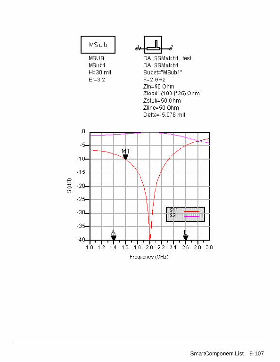
SmartComponent List 9-107
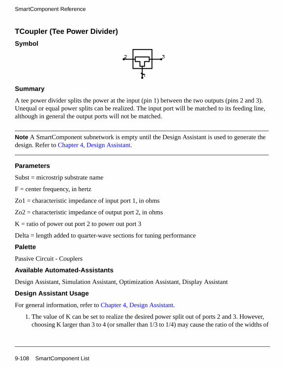
SmartComponent Reference
TCoupler (Tee Power Divider)
Symbol
Summary
A tee power divider splits the power at the input (pin 1) between the two outputs (pins 2 and 3).Unequal or equal power splits can be realized. The input port will be matched to its feeding line,although in general the output ports will not be matched.
Note A SmartComponent subnetwork is empty until the Design Assistant is used to generate thedesign. Refer to Chapter 4, Design Assistant.
Parameters
Subst = microstrip substrate name
F = center frequency, in hertz
Zo1 = characteristic impedance of input port 1, in ohms
Zo2 = characteristic impedance of output port 2, in ohms
K = ratio of power out port 2 to power out port 3
Delta = length added to quarter-wave sections for tuning performance
Palette
Passive Circuit - Couplers
Available Automated-Assistants
Design Assistant, Simulation Assistant, Optimization Assistant, Display Assistant
Design Assistant Usage
For general information, refer to Chapter 4, Design Assistant.
1. The value of K can be set to realize the desired power split out of ports 2 and 3. However,choosing K larger than 3 to 4 (or smaller than 1/3 to 1/4) may cause the ratio of the widths of
9-108 SmartComponent List

the tee branches to violate the range of the MTEE simulation model. While the simulationwill still proceed, the results may have some inaccuracies.
2. Quarter-wave matching sections are provided on the output ports to ensure a proper powersplit is achieved.
3. For a more detailed discussion of this device, see: D. M. Pozar, Microwave Engineering,2nd Edition, John Wiley & Sons: New York, 1998, pp. 360-361.
Simulation Assistant Usage
For general information, refer to Chapter 5, Simulation Assistant.
Optimization Assistant Usage
For general information, refer to Chapter 6, Optimization Assistant.
The optimization minimizes the input reflection coefficient (S11) at the design center frequency bychanging the length of the quarter wave transformers on the output legs.
Display Assistant Usage
For general information, refer to Chapter 7, Display Assistant.
Example
A tee power divider was designed for a center frequency of 1GHz with an unequal power split (K= 3.5). Tuning using the Optimization Assistant yielded a value of Delta = -34.633 mil.
SmartComponent List 9-109
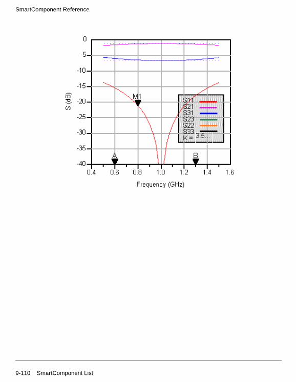
SmartComponent Reference
9-110 SmartComponent List
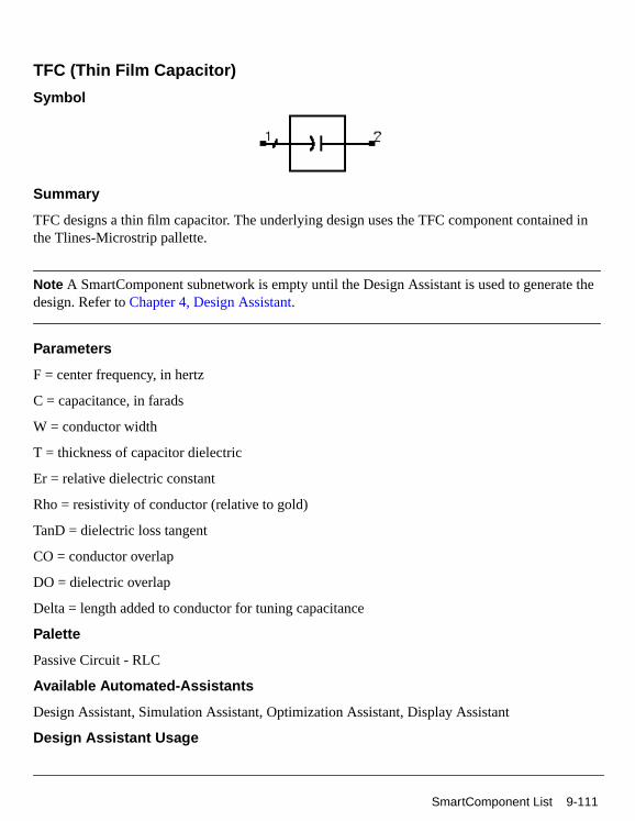
TFC (Thin Film Capacitor)
Symbol
Summary
TFC designs a thin film capacitor. The underlying design uses the TFC component contained inthe Tlines-Microstrip pallette.
Note A SmartComponent subnetwork is empty until the Design Assistant is used to generate thedesign. Refer to Chapter 4, Design Assistant.
Parameters
F = center frequency, in hertz
C = capacitance, in farads
W = conductor width
T = thickness of capacitor dielectric
Er = relative dielectric constant
Rho = resistivity of conductor (relative to gold)
TanD = dielectric loss tangent
CO = conductor overlap
DO = dielectric overlap
Delta = length added to conductor for tuning capacitance
Palette
Passive Circuit - RLC
Available Automated-Assistants
Design Assistant, Simulation Assistant, Optimization Assistant, Display Assistant
Design Assistant Usage
SmartComponent List 9-111

SmartComponent Reference
For general information, refer to Chapter 4, Design Assistant.
1. The design is accomplished by determining the length required to achieve the desiredcapacitance using the simple parallel plate capacitor model C = Er*W*L/T. The parametersfrom Rho through DO inclusive are not used in the design process but are passed on to theunderlying TFC component and are therefore included in any simulations or optimizations.
2. The tuning parameter Delta represents incremental length required to achieve the desiredcapacitance. It is typically relatively small, as the initial design tends to be accurate.
Simulation Assistant Usage
For general information, refer to Chapter 5, Simulation Assistant.
Optimization Assistant Usage
For general information, refer to Chapter 6, Optimization Assistant.
The Optimization Assistant tunes the conductor length to achieve the desired capacitance.
Display Assistant Usage
For general information, refer to Chapter 7, Display Assistant.
Example
A TFC component was used to design a 1 pF capacitor at a center frequency of 5 GHz using adielectric with a 0.2 mil thickness and dielectric constant of 9.6. Optimization yielded a value ofDelta = -0.000178 mil.
9-112 SmartComponent List

SmartComponent List 9-113

SmartComponent Reference
TFR (Thin Film Resistor)
Symbol
Summary
TFR designs a thin film resistor. The underlying design uses the TFR component contained in theTlines-Microstrip pallette.
Note A SmartComponent subnetwork is empty until the Design Assistant is used to generate thedesign. Refer to Chapter 4, Design Assistant.
Parameters
Subst = microstrip substrate name
F = center frequency, in hertz
R = resistance, in ohms
W = conductor width (set to 0 if Zo specified)
Zo = characteristic impedance of line assuming Rs = 0 (set to 0 if W specified)
Rs = sheet resistivity, in ohms/square
CO = conductor overlap
Delta = length added to conductor for tuning resistance
Palette
Passive Circuit - RLC
Available Automated-Assistants
Design Assistant, Simulation Assistant, Optimization Assistant, Display Assistant
Design Assistant Usage
For general information, refer to Chapter 4, Design Assistant.
1. The design is accomplished by determining the length required to achieve the desiredresistance using the sheet resistivity Rs in conjunction with the strip width W. The
9-114 SmartComponent List
parameters Freq and CO are not used in the design process but are passed on to theunderlying TFR component and are therefore included in any simulations or optimizations.
2. Since this resistor is often fed with a microstrip line, either the physical width or thecharacteristic impedance of a microstrip line on the substrate can be specified.
3. The tuning parameter Delta represents incremental length required to achieve the desiredresistance.
Simulation Assistant Usage
For general information, refer to Chapter 5, Simulation Assistant.
Optimization Assistant Usage
For general information, refer to Chapter 6, Optimization Assistant.
The Optimization Assistant tunes the conductor length to achieve the desired resistance.
Display Assistant Usage
For general information, refer to Chapter 7, Display Assistant.
Example
A TFR component was used to design a 50 ohm resistor at a center frequency of 5 GHz using aconductor with a sheet resistance of 50 ohm/square. The conductor width was chosen tocorrespond to that of a 50 ohm microstrip line on the substrate. Optimization yielded a value ofDelta = -3.549 mil.
SmartComponent List 9-115
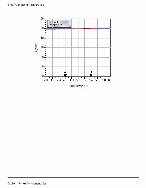
SmartComponent Reference
9-116 SmartComponent List

TLMatch (Tapered-Line Match)
Symbol
Summary
A tapered-line matching network matches a real load impedance (Rload) to a desired real inputimpedance (Zo) using a continuously varying line characteristic impedance to realize a specifiedfrequency response. The reflection coefficient remains below the specified maximum value for allfrequencies above the design frequency.
Note A SmartComponent subnetwork is empty until the Design Assistant is used to generate thedesign. Refer to Chapter 4, Design Assistant.
Parameters
Subst = microstrip substrate name
F = design frequency, in hertz
Zo = desired input impedance, in ohms
Rload = load impedance to match, in ohms
ResponseType = type of frequency response (exponential, triangular, Klopfenstein)
L = length of tapered line in wavelengths at frequency F(set L=0 to compute L)
Rmax = maximum voltage reflection coefficient
NSection = number of linear taper sections per wavelength
Palette
Passive Circuit - Matching
Available Automated-Assistants
Design Assistant, Simulation Assistant, Optimization Assistant, Display Assistant
Design Assistant Usage
For general information, refer to Chapter 4, Design Assistant.
SmartComponent List 9-117

SmartComponent Reference
1. The continuous impedance taper of this circuit is approximated using a sequence of lineartapers. Increasing the number of sections per wavelength (NSection) will improve theapproximation to the defined taper.
2. If the length of the line L is set to zero, the Design Assistant chooses L such that thereflection coefficient is less than Rmax for all frequencies above the design frequency.Otherwise, Rmax is ignored.
3. The ResponseType specifies the distribution of the impedance along the length of the lineand therefore determines the frequency response of the match.
4. For a more detailed discussion of this device, see: D. M. Pozar, Microwave Engineering,2nd Edition, John Wiley & Sons: New York, 1998, pp. 288-295.
Simulation Assistant Usage
For general information, refer to Chapter 5, Simulation Assistant.
Optimization Assistant Usage
For general information, refer to Chapter 6, Optimization Assistant.
No Optimization Assistant is provided since the design process is exact to within theapproximation of the continuous impedance taper using multiple linear taper segments. Increasingthe value of NSection will improve the computed response.
Display Assistant Usage
For general information, refer to Chapter 7, Display Assistant.
Example
A tapered-line matching network was designed to match a load impedance of 100 ohms to a 50ohm line at a center frequency of 4 GHz. Specifying a Klopfenstein frequency response for whichthe reflection coefficient remains below 0.1 along with 30 sections per wavelength dictates 18tapered-line sections to realize the match. The plot has been shown in linear magnitude rather thandB to emphasize the equal-ripple frequency response.
9-118 SmartComponent List
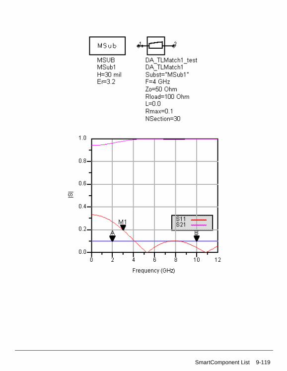
SmartComponent List 9-119

SmartComponent Reference
WDCoupler (Wilkinson Divider)
Symbol
Summary
A Wilkinson power divider splits the power at the input (pin 1) between the two outputs (pins 2and 3). Unequal or equal power splits can be realized. The signals at the outputs are in phase. Allthree ports will be matched, and ports 2 and 3 will in general be well isolated from each other.
Note A SmartComponent subnetwork is empty until the Design Assistant is used to generate thedesign. Refer to Chapter 4, Design Assistant.
Parameters
Subst = microstrip substrate name
F = center frequency, in hertz
Zo = characteristic impedance, in ohms
K = ratio of power out port 2 to power out port 3
Wgap = width of gap for resistor
Delta = length added to quarter-wave branches for tuning performance
Palette
Passive Circuit - Couplers
Available Automated-Assistants
Design Assistant, Simulation Assistant, Optimization Assistant, Display Assistant
Design Assistant Usage
For general information, refer to Chapter 4, Design Assistant.
1. The value of K can be set to realize the desired power split out of ports 2 and 3. However,choosing K larger than 3 to 4 (or smaller than 1/3 to 1/4) may cause difficulties in thedesign.
9-120 SmartComponent List
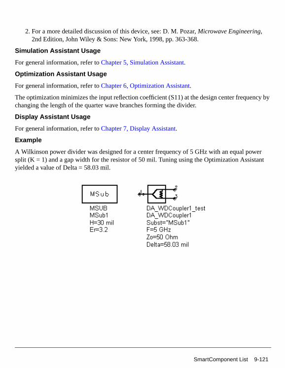
2. For a more detailed discussion of this device, see: D. M. Pozar, Microwave Engineering,2nd Edition, John Wiley & Sons: New York, 1998, pp. 363-368.
Simulation Assistant Usage
For general information, refer to Chapter 5, Simulation Assistant.
Optimization Assistant Usage
For general information, refer to Chapter 6, Optimization Assistant.
The optimization minimizes the input reflection coefficient (S11) at the design center frequency bychanging the length of the quarter wave branches forming the divider.
Display Assistant Usage
For general information, refer to Chapter 7, Display Assistant.
Example
A Wilkinson power divider was designed for a center frequency of 5 GHz with an equal powersplit (K = 1) and a gap width for the resistor of 50 mil. Tuning using the Optimization Assistantyielded a value of Delta = 58.03 mil.
SmartComponent List 9-121

SmartComponent Reference
9-122 SmartComponent List
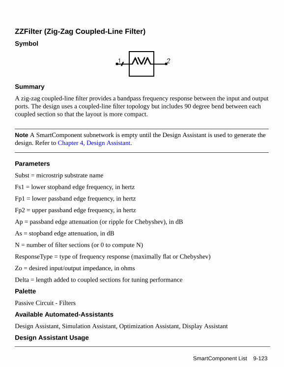
ZZFilter (Zig-Zag Coupled-Line Filter)
Symbol
Summary
A zig-zag coupled-line filter provides a bandpass frequency response between the input and outputports. The design uses a coupled-line filter topology but includes 90 degree bend between eachcoupled section so that the layout is more compact.
Note A SmartComponent subnetwork is empty until the Design Assistant is used to generate thedesign. Refer to Chapter 4, Design Assistant.
Parameters
Subst = microstrip substrate name
Fs1 = lower stopband edge frequency, in hertz
Fp1 = lower passband edge frequency, in hertz
Fp2 = upper passband edge frequency, in hertz
Ap = passband edge attenuation (or ripple for Chebyshev), in dB
As = stopband edge attenuation, in dB
N = number of filter sections (or 0 to compute N)
ResponseType = type of frequency response (maximally flat or Chebyshev)
Zo = desired input/output impedance, in ohms
Delta = length added to coupled sections for tuning performance
Palette
Passive Circuit - Filters
Available Automated-Assistants
Design Assistant, Simulation Assistant, Optimization Assistant, Display Assistant
Design Assistant Usage
SmartComponent List 9-123
SmartComponent Reference
For general information, refer to Chapter 4, Design Assistant.
1. Because of the heavy computational burden in determining the line parameters, a brief delaywill occur for the design.
2. For a Chebyshev (equal ripple) frequency response, ripple levels greater than about 1 dB arenot recommended. Exceeding this value will typically deform the shape of the passbandcharacteristics.
3. If N is zero, the number of filter sections will be computed from the frequency/attenuationinformation. If N is non-zero, the design will use the frequency/attenuation parameters onlyfor determining the design center frequency.
4. For a more detailed discussion of this device, see: D. M. Pozar, Microwave Engineering,2nd Edition, John Wiley & Sons: New York, 1998, pp. 477-485.
Simulation Assistant Usage
For general information, refer to Chapter 5, Simulation Assistant.
Optimization Assistant Usage
For general information, refer to Chapter 6, Optimization Assistant.
The optimization minimizes the absolute difference between S21 and the specified passband edgeattenuation (which equals the ripple for Chebyshev response) at the passband edge frequencies.Because only the line lengths are changed, this tuning will typically center the response within thespecified passband. More advanced shaping of the passband response can be accomplished bymanually tuning the widths and spacings of the coupled filter sections.
Display Assistant Usage
For general information, refer to Chapter 7, Display Assistant.
Example
A zig-zag coupled-line filter was designed for a maximally flat response with the 3 dB passbandedge frequencies at 2 GHz and 2.4 GHz respectively. The design required 4 coupled-line sections.Tuning using the Optimization Assistant yielded a value of Delta = -6.233 mil.
9-124 SmartComponent List

SmartComponent List 9-125

SmartComponent Reference
9-126 SmartComponent List
Index
BBLCoupler, 9-4CCLCoupler, 9-7CLFilter, 9-10CMFilter, 9-13
DDesignGuide QuickStarts
Passive Circuit, 1-1DSMatch, 9-16
HHPFilter, 9-19
IIDFilter, 9-22
LLCoupler, 9-25LEMatch, 9-28
MMBend, 9-31MBStub, 9-33MCFil, 9-36MCLine, 9-38MCorn, 9-40MCross, 9-41MCurve, 9-43MGap, 9-45MICapP, 9-46MICapPG, 9-49MICapS, 9-52MICapSG, 9-55MLine, 9-58MMndr, 9-60MREInd, 9-63MRInd, 9-66MRStub, 9-69MSInd, 9-72MStep, 9-75MStub, 9-76MTaper, 9-78MTee, 9-80
MTFC, 9-82
PPassive Circuit DesignGuide
Control Window (using), 1-8coupler components, 9-2creating artwork, 8-1Design Assistant (using), 4-1design flow, 1-15Display Assistant (using), 7-1distributed capacitor components, 9-1distributed inductor components, 9-2distributed resistor components, 9-2divider components, 9-2filter components, 9-2How Do I?, 2-1layout generation, 8-1line components, 9-1matching network components, 9-3navigation, 1-5Optimization Assistant (using), 6-1QuickStart, 1-1simple examples, 1-10Simulation Assistant (using), 5-1Smart component Reference, 9-1updating layouts, 8-1
QQWMatch, 9-85
RRRCoupler, 9-88
SSBFilter, 9-91SIFilter, 9-95SLFilter, 9-98SRFilter, 9-102SSMatch, 9-105
TTCoupler, 9-108TFC, 9-111TFR, 9-114TLMatch, 9-117
Index-1

WWDCoupler, 9-120
ZZZFilter, 9-123
-2


![Optimizing Embedded Passive Content in Printed Circuit Boardsescml.umd.edu/Papers/Bevin_EmbeddedPasOpt.pdf · components, e.g., a printed circuit board - PCB), [1]. Embedding passives](https://static.documents.pub/doc/80x56/5e8508e9cf1918070d7b6c87/optimizing-embedded-passive-content-in-printed-circuit-components-eg-a-printed.jpg)


