ÎÎ Notebook, Desktop computersÎÎ Displays, MonitorsÎÎ A/V receivers, Set Top Box, Video PlayersÎÎ Repeaters and switch boxes
Figure 1-1 DP++ Level Shifter in Notebook PC
Figure 1-2 HDMI Port in All-In-One PC
Ordering Information
Ordering Number Package Code Package Description
PI3HDX511FZLCEX ZLC 40-pin, 3x6mm (TQFN)
PI3HDX511FZLCIEX ZLC 40-pin, 3x6mm (TQFN)Notes:1. No purposely added lead. Fully EU Directive 2002/95/EC (RoHS), 2011/65/EU (RoHS 2)
& 2015/863/EU (RoHS 3) compliant. 2. See https://www.diodes.com/quality/lead-free/ for more information about Diodes
Incorporated’s definitions of Halogen- and Antimony-free, "Green" and Lead-free. 3. Halogen- and Antimony-free "Green” products are defined as those which contain
<900ppm bromine, <900ppm chlorine (<1500ppm total Br + Cl) and <1000ppm anti-mony compounds.
4. E = Pb-free and Green5. X suffix = Tape/Reel
Description
PI3HDX511F is a ultra-low power HDMI 1.4b ReDriver and dual-mode DisplayPort level shifter up to 3.4Gbps data rate with48-bpp Deep Color support.In the mobile platforms, extending battery hours have been one of the most challenges for system designers. PI3HDX511F has rich power saving features to extend the battery life with 2uA stand-by current and other features like LDO disable pins, Ative/Passive DDC switch, Output squelch and HPD (Hot plug Detect) detection.PI3HDX511F can support both source and sink side system application. For Sink side (Recepticle) application, it supports 6-step input EQ adjustment and data/clock pin order swap.
Features
Î Ultra-low power HDMI 1.4b compliant Redriver Î Dual-mode DisplayPort Level Shifter/Redriver with pin option
Î Operation up to 3.4 Gbps per lane ( 340MHz pixel clock) Î Sink-side application support with TMDS Data & Clock pin swaps and high 15dB EQ options
Î 4K2K Ultra-HD, 3D Video formats (1080p, 1080i, 720p), 48-bit per pixel Deep Color support
Î Ultra-low standby current 2uA with DDC passive switch mode
Î Flexible 6 steps input equalization control steps: 2.5/5/7.5 dB for short cable range and 5/10/15 dB for long cable modes.
Î Pre-emphasis 3 steps setting: 0/1.5/2.5 dB Î Automatic TMDS output disable with squelch or HPD detection in the no-signal input condition
Î Selectable Active DDC buffer mode for 1.8-3.3V DDC Î Max 120mW with LDO Bypass 1.5V power supply mode Î Integrated ESD protection: 8kV HBM for all IO pins per JEDEC standard
Î Power supply: 3.3V single or 3.3/1.5V dual power supply Î Totally Lead-Free & Fully RoHS Compliant (Notes 1 & 2) Î Halogen and Antimony Free. “Green” Device (Note 3) Î For automotive applications requiring specific change control (i.e. parts qualified to AEC-Q100/101/200, PPAP capable, and manufactured in IATF 16949 certified facilities), please contact us or your local Diodes representative.
June 2016 P10 - Add Eye opening measurement with different test set-up in the functional description. Expand I-temp grade support in the ordering information.
July 2016 Add more contents to assist the system design-in in Application page 20 eg. PCB layout, HDMI compliance report.
Sep 2016Add clarity for the total power dissipation in the Open-drain and the Double termination modes in p1, p12 andp13.
Feb 2017 Add Via in the package mechanical drawingJun 2017 I-temp ordering part number added . Diodes Datasheet style updated.Nov 2017 Package outline drawing updated.Aug 2018 Remove HDMI active cable/dongle application.Nov 2020 Updated Package from ZL Package to ZLC Package
PI3DPX1203B 8.1Gbps Displayport 1.4 Linear Redriver. Low-jitter, Latency Free.PI3HDX1204B1 6Gbps HDMI 2.0 Redriver and Displayport Level Shifter, Low-jitter, High EQ.PI3HDX414 1:4 Active 3.4Gbps HDMI 1.4b Splitter/DeMux with Signal ConditioningPI3HDX412BD 1:2 Active 3.4Gbps HDMI 1.4b Splitter/DeMux with Signal ConditioningPI3HDX621 2:1 Active 3.4Gbps HDMI 1.4b SwitchPI3HDMI336 3:1 Active 2.5Gbps HDMI Switch with I2C control and ARC TransmitterPI3DPX1202 5.4Gbps Displayport 1.2 Redriver with built-in auto test modePI3WVR12612 Wide Voltage Range DisplayPort™ & HDMI Video 1:2 Mux/DeMux
Advanced Formative / In Design Datasheet contains the design specifications for product development. Specifications may change in any manner without notice.
Preliminary First ProductionDatasheet contains preliminary data; supplementary data will be published at a later date. Diodes Incorporated reserves the right to make product specification changes at any time without notice to improve design.
No Identification Needed Full Production
Datasheet contains final specifications. Diodes Incorporated reserves the right to make changes at any time without notice to improve datasheet informative or reference contents.
Obsolete Not In Production Datasheet contains specifications on a product that is discontinued by Diodes Incorporated. The datasheet is for reference information only.
1. Product Summary ....................................................................................................................................................... 12. General Information .................................................................................................................................................. 2
2.1 Revision History .................................................................................................................................................... 22.2 Products Comparsion .......................................................................................................................................... 22.3 Related Products .................................................................................................................................................... 32.4 Reference Document ............................................................................................................................................ 32.5 Product Status Definition .................................................................................................................................... 3
7. Mechanical, Ordering Information .................................................................................................................... 327.1 Mechanical Outline ............................................................................................................................................. 327.2 Part Marking Information ................................................................................................................................ 337.3 Tape & Reel Materials and Design .................................................................................................................. 34
8. Important Notice ....................................................................................................................................................... 37
1, 7, 29 VDD PWR 3.3V power supply. Add external 0.1uF decoupling capacitor to GND.
2 CEXT/VDD15 PWR
LDO output for internal core power supplier.VDD15: When LDO_EN is low "0", this shared pin be a VDD15 in dual power supply operation. Apply 1.5V powerCEXT: When LDO_EN is high "1", this pin be a CEXT in 3.3V single power supply operation. Add external capacitor (2.2uF-4.7uF) to GND.
3 IN_D2- I TMDS inputs. RT=50Ω and RPD=200 kΩ.4 IN_D2+ I TMDS inputs. RT=50Ω and RPD=200 kΩ.5 IN_D1- I TMDS inputs. RT=50Ω and RPD=200 kΩ.6 IN_D1+ I TMDS inputs. RT=50Ω and RPD=200 kΩ.8 IN_D0- I TMDS inputs. RT=50Ω and RPD=200 kΩ.9 IN_D0+ I TMDS inputs. RT=50Ω and RPD=200 kΩ.10 IN_CLK- I TMDS inputs. RT=50Ω and RPD=200 kΩ.11 IN_CLK+ I TMDS inputs. RT=50Ω and RPD=200 kΩ.12 HPD_SRC O HPD output to source side
13 TMDS_ORDER I TMDS pin order swap control with internal pull high. Default is D2/D1/D0/CLK input sequence.
14 HPDO_S0 I HPD_SRC output control with internal pull high. Default is Open drain output15, 18, 37, 39, Center Pad
GND GND Ground
16 SDA_SRC IO Source side DDC Data17 SCL_SRC IO Source side DDC Clock
19 ROUT_S0 ITMDS output enable with double termination or open-drain selection. Default is Active high, double termination output. Active low is open-drain output. Internal pull high to VDD.
20 OC_S0 I TMDS output pre-emphasis value selection. Default is 1.5dB pre-emphasis setting. Inter-nally tied with 50% of VDD (or VDD/2).
21 DDC_SEL I DDC buffer or Passive switch control. Default is Passive switch mode. Internal pull high.
22 VBIAS I TMDS input termination voltage control. Default is HDMI input mode. Internally pull high. Pull-down is for Displayport input mode.
23 EQ_STEP I EQ_step selection control. Default is low-side setting of 2.5/5/7.5dB. Internally pull high. High-side EQ values are 5/10/15dB with external pull-down.
24 EQ_S0 I TMDS input three-level equalization selection. Default is middle EQ value setting. Inter-nally 50% of VDD (VDD/2).
25 OUT_CLK+ O TMDS outputs with ROUT=50Ω, when ROUT_S0= "1"26 OUT_CLK- O TMDS outputs with ROUT=50Ω, when ROUT_S0= "1"27 OUT_D0+ O TMDS outputs with ROUT=50Ω, when ROUT_S0= "1"28 OUT_D0- O TMDS outputs with ROUT=50Ω, when ROUT_S0= "1"
30 OUT_D1+ O TMDS outputs with ROUT=50Ω, when ROUT_S0= "1"31 OUT_D1- O TMDS outputs with ROUT=50Ω, when ROUT_S0= "1"32 OUT_D2+ O TMDS outputs with ROUT=50Ω, when ROUT_S0= "1"33 OUT_D2- O TMDS outputs with ROUT=50Ω, when ROUT_S0= "1"34 SCL_SINK IO Sink side DDC Clock for connector35 SDA_SINK IO Sink side DDC Data for connector
36 HPD_SINK I Sink side HPD (Hot Plug Detect) input. Active high pin. Default is inactive for power saving. Internally pull-down at 120 kOhm.
38 OEB I Output Enable control. Active low for normal operation. Active high for disable output HDMI signals. Internally pull-down with 100 kΩ.
40 LDO_EN IPower supply mode control pin for 1.5/3.3V or 3.3VDefault is 3.3V operation with active high. Internally pull high. 1.5/3.3V dual power is active low.
4.2 Function DescriptionSquelch ModeAutomatic output squelch function disables TMDS output when no Input signal presents. Output Disable (Squelch) Mode uses TMDS Clock signal detection. When low voltage levels on the TMDS input clock are detected, Squelch state enables and TMDS outputs shall be disabled. When the TMDS clock inputs are above the pre-determined threshold voltage, TMDS outputs shall return to the normal swing voltage levels.
TMDS Output Shut DownWhen HPD_SINK pin floats or ties to GND, TMDS outputs shall shut down to sleep mode; HPD_SINK does not control DDC channel. TMDS Pin Order Configuration TableTMDS_ORDER Functional Description Note"0" CLK/D0/D1/D2 pin order"1" or "NC" D2/D1/D0/CLK pin order Default
DDC mode selection DDC_SEL Configuration TableDDC_SEL Functional Description Note"0" Active DDC Buffer"1" or "NC" Passive Switch Default
Pre-emphasis Truth TableROUT_S0 OC_S0 Single-end Vswing Pre-emphasis Functional Description"0" "0" 500 mV 0 dB Open drain output.
"NC" or VDD/2 500 mV 1.5 dB Open drain output(Default)"1" 500 mV 2.5 dB Open drain output
"1" "0" 500 mV 0 dB Double termination"NC" or VDD/2 500 mV 1.5 dB Double termination(Default)"1" 500 mV 2.5 dB Double termination
TMDS Input Termination Voltage Control VBIASVBIAS Functional Description"1", "NC" HDMI input. VBIAS ties to VDD."0" DisplayPort input. VBIAS ties to GND.
EQ Step Selection Control EQ_STEPEQ_STEP Functional Description"1", "NC" 2.5, 5, 7.5dB EQ setting with EQ_S0 control pin"0" 5, 10, 15dB EQ setting with EQ_S0 control pin
Output Data Signals EQ_S0 ConfigurationEQ_S0 Functional Description Note
EQ_STEP = "1" EQ_STEP = "0""0" 2.5 dB 5 dB TMDS Clock(CLK) channel EQ is always fixed as
3dB without pre-emphasis."NC" , "VDD/2" 5 dB 10 dB"1" 7.5 dB 15 dB
Sink side Hot Plug Detect HPD_SINKEQ_STEP Functional Description"1" Normal mode"0" Disable output signal for power saving mode
Source side Hot Plug Detect Output Control HPDO_S0EQ_STEP Functional Description"1" or "NC" Open drain output (Default)"0" Inverted Buffer output of HPD_SINK signal
Output Enable Control Truth TableEQ_STEP Functional Description"0" Active Low. Normal mode"1" Disable output signal for power saving mode PI3HDX511FA
Note:(1) Stresses greater than those listed under MAXIMUM RATINGS may cause permanent damage to the device. This is a stress rating only and functional opera-
tion of the device at these or any other conditions above those indicated in the operational sections of this specification is not implied. Exposure to beyond the absolute maximum rating conditions for extended periods may affect inoperability and degradation of device reliability and performance.
5.2 Recommended Operation Conditions
Symbol Parameter(1) Min. Typ. Max. Unit
VDD Power Supply Voltage2.89 3.3 3.6 V
1.42 1.5 1.57 V
TAAmbient Operating Temperature 0 70 oC
Industrial Operating Temperature -40 85 oC
Note (1) Industrial temperature -40 to +85 oC can be guaranteed by design. Commercial temperature 0 to +70 oC is supported by the production-tested.
5.3 Electrical Characteristics5.3.1 DC ElectricalPower Consumption
Symbol Parameter Conditions Min. Typ. Max. Unit
Single Power Supply
IDD33 3.3V Power @ 0dB Pre-Emp
Outputs Enable (open drain 500mV, 0 dB pre-emphasis). terminated OUT_D [0:2] and CLK with 50 ohms to VDD. Exclude 40mA current pass-through from source devices
110 mA
IDD33 3.3V Power@ 0dB Pre-Emp
Outputs Enable (Double termination 500mV, 0 dB pre-emphasis). terminated OUT_D [0:2] and CLK with 50 ohms to VDD. Exclude 40mA current pass-through from source devices
Outputs Enable (Open Drain 500mV, 2.5 dB pre-emphasis). terminated OUT_D [0:2] and CLK with 50 ohms to VDD. Exclude 40mA current pass-through from source devices
133 mA
IDD33 3.3V Power @ 2.5dB Pre-Emp
Outputs Enable (Double termination 500mV, 2.5 dB pre-emphasis). terminated OUT_D [0:2] and CLK with 50 ohms to VDD. Exclude 40mA current pass-through from source devices
211 mA
Dual Power Supply
IDD15
1.5V @ open drain 500mV, 0dBOutputs Enable (open drain 500mV, 0dB pre-emphasis), terminated OUT_D [0:2] and CLK with 50 ohms to Vdd
58 70 mA
1.5V @ double termination 500mV, 0dBOutputs Enable (open drain 500mV, 0dB pre-emphasis), terminated OUT_D [0:2] and CLK with 50 ohms to Vdd
78.2 mA
1.5V @ double termination 500mV, 2.5dBOutputs Enable (open drain 500mV, 0dB pre-emphasis), terminated OUT_D [0:2] and CLK with 50 ohms to Vdd
DDC active buffer ( open drain & double termination); OEB = 1, HPD_SINK = 0
1.5 mA
DDC Passive Switch ( open drain & double termination); OEB= 1 and HPD_SINK = 0
0 mA
DDC active buffer ( open drain & double termination); OEB= 0 and HPD_SINK = 0
1.44 mA
Squelch Current
ISQLH Squelch mode current; VDD = 3.6V
DDC passive switch; No input clock VDD=3.6V, HPD_SINK=3.6V
2.68 3.0 mA
DDC active buffer; No input clock VDD=3.6V, HPD_SINK=3.6V
3.52 4.1 mA
Note:1. Current is due to internal 100kΩ pull-down of OE pin drawing extra current (~36uA). If forced by a separate power supply with all other control pins open,
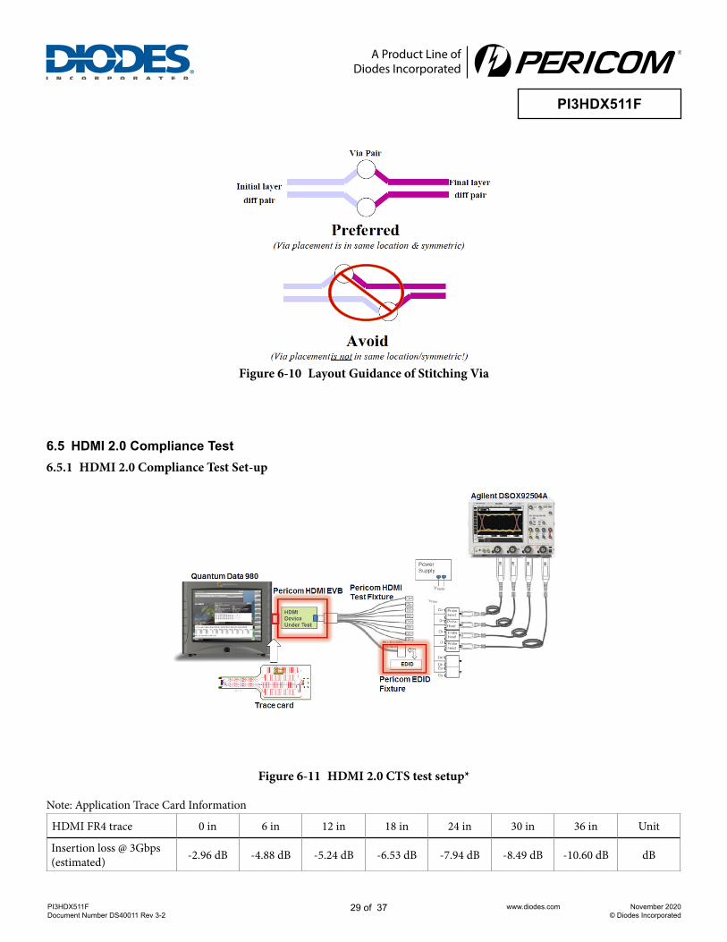
6.3 Output Eye Measurement DataSink Apps test set-up: Output Eye Diagram with different EQ settings of 1.5dB, 10dB and 15 dB. Trace Cards used with 24”, 48” and 84” with 2 meter HDMI Cable with proper pre-emphasis setting.
Note: For system designers reference, AE-trace board information are shown below. Insertion loss is measured in the 3GHz (6.0 Gbps) speed.
6.4 Layout GuidelinesAs transmission data rate increases rapidly, any flaws and/or mis-matches on PCB layout are amplified in terms of signal integrity.Layout guideline for high-speed transmission is highlighted in this application note.
6.4.1 Power and Ground
To provide a clean power supply for Pericom high-speed device, few recommendations are listed below:
• Power (VDD) and ground (GND) pins should be connected to corresponding power planes of the printed circuit board directly without passing through any resistor.
• The thickness of the PCB dielectric layer should be minimized such that the VDD and GND planes create low inductance paths.• One low-ESR 0.1uF decoupling capacitor should be mounted at each VDD pin or should supply bypassing for at most two VDD
pins. Capacitors of smaller body size, i.e. 0402 package, is more preferable as the insertion loss is lower. The capacitor should be placed next to the VDD pin.
• One capacitor with capacitance in the range of 4.7uF to 10uF should be incorporated in the power supply decoupling design as well. It can be either tantalum or an ultra-low ESR ceramic.
• A ferrite bead for isolating the power supply for Pericom high-speed device from the power supplies for other parts on the printed circuit board should be implemented.
• Several thermal ground vias must be required on the thermal pad. 25-mil or less pad size and 14-mil or less finished hole are rec-ommended.
G N D P la ne
VIN
V DD P la ne
10uF
1uF
0.1uF
0.1uF
0.1uF
Bypass noisePower Flow
VIN
VIN
Center PadGND Plane
Several Thermal GND Vias must be required on the Thermal Pad area
6.4.2 High-speed signal RoutingWell-designed layout is essential to prevent signal reflection:
• For 90Ω differential impedance, width-spacing-width micro-strip of 6-7-6 mils is recommended; for 100Ω differential impedance, width-spacing-width micro-strip of 5-7-5 mils is recommended.
• Differential impedance tolerance is targeted at ±15%.
Figure 6-2 Trace Width and Clearance of Micro-strip and Strip-line
• For micro-strip, using 1/2oz Cu is fine. For strip-line in 6+ PCB layers, 1oz Cu is more preferable.
• To keep the reference unchanged, stitching vias must be used when changing layers.• Differential pair should maintain symmetrical routing whenever possible. The intra-pair skew of micro-strip should be less than
5 mils.
• To keep the reference unchanged, stitching vias must be used when changing layers.• Differential pair should maintain symmetrical routing whenever possible. The intra-pair skew of micro-strip should be less than
5 mils.
Figure 6-6 Layout Guidance of Matched Differential Pair
• For minimal crosstalk, inter-pair spacing between two differential micro-strip pairs should be at least 20 mils or 4 times the dielec-tric thickness of the PCB.
• Wider trace width of each differential pair is recommended in order to minimize the loss, especially for long routing. More consis-tent PCB impedance can be achieved by a PCB vendor if trace is wider.
• Differential signals should be routed away from noise sources and other switching signals on the printed circuit board.• To minimize signal loss and jitter, tight bend is not recommended. All angles α should be at least 135 degrees. The inner air gap A
should be at least 4 times the dielectric thickness of the PCB.
7.2 Part Marking InformationOur standard product mark follows our standard part number ordering information, except for those products with a speed letter code. The speed letter code mark is placed after the package code letter, rather than after the device number as it is ordered. After electrical test screening and speed binning has been completed, we then perform an “add mark” operation which places the speed code letter at the end of the complete part number.
PI X1 X2X3X4 X5X6X7X8X9
Product IO Configurationi.e) X5X6= Data Speed, X7=Total IO ports, X8= Port in, X9= Port out
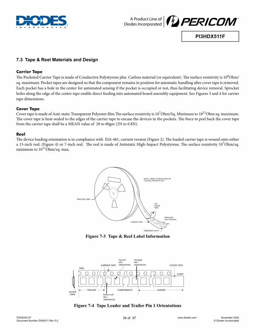
Carrier TapeThe Pocketed Carrier Tape is made of Conductive Polystyrene plus Carbon material (or equivalent). The surface resistivity is 106Ohm/sq. maximum. Pocket tapes are designed so that the component remains in position for automatic handling after cover tape is removed. Each pocket has a hole in the center for automated sensing if the pocket is occupied or not, thus facilitating device removal. Sprocket holes along the edge of the center tape enable direct feeding into automated board assembly equipment. See Figures 3 and 4 for carrier tape dimensions.
Cover TapeCover tape is made of Anti-static Transparent Polyester film.The surface resistivity is 107Ohm/Sq. Minimum to 1011Ohm sq. maximum. The cover tape is heat-sealed to the edges of the carrier tape to encase the devices in the pockets. The force to peel back the cover tape from the carrier tape shall be a MEAN value of 20 to 80gm (2N to 0.8N).
ReelThe device loading orientation is in compliance with EIA-481, current version (Figure 2). The loaded carrier tape is wound onto either a 13-inch reel, (Figure 4) or 7-inch reel. The reel is made of Antistatic High-Impact Polystyrene. The surface resistivity 107Ohm/sq. minimum to 1011Ohm/sq. max.
NOTE: LABELS TO BE PLACED ON THE REEL OPPOSITE PIN 1
TOP COVER TAPE
SPROCKET HOLE (ROUND)
CARRIER TAPE
EMBOSSED CAVITY
BARCODE LABEL
Figure 7-3 Tape & Reel Label Information
ENDCARRIER TAPE
TRAILERCOVERTAPE
COMPONENTS
COVER TAPE
START
LEADER
Top LeftPIN 1ORIENTATION
Top RightPIN 1ORIENTATION
Bottom LeftPIN 1ORIENTATION
Figure 7-4 Tape Leader and Trailer Pin 1 Orientations
NOTES:1. A0, B0, and K0 are determined by component size. The cavity must restrict lateral movement of component to 0.5mm maximum for 8mm and 12mm wide tape and to 1.0mm maximum for 16,24,32, and 44mm wide carrier. The maximum component rotation within the cavity must be limited to 20o maximum for 8 and 12 mm carrier tapes and 10o maximum for 16 through 44mm. 2. Tape and components will pass around reel with radius “R” without damage.3. S1 does not apply to carrier width ≥32mm because carrier has sprocket holes on both sides of carrier where Do≥S1. 4. So does not exist for carrier ≤32mm because carrier does not have sprocket hole on both side of carrier.
Table 7-3. Reel dimensions by tape sizeTape Size A N (Min)
See Note A W1 W2(Max) W3 B (Min) C D (Min)
8mm 178 ±2.0mm or 330±2.0mm
60 ±2.0mm or 100±2.0mm
8.4 +1.5/-0.0 mm 14.4 mm
Shall Ac-commodate Tape Width
Without Interference
1.5mm 13.0 +0.5/-0.2 mm 20.2mm
12mm 12.4 +2.0/-0.0 mm 18.4 mm16mm
330 ±2.0mm 100 ±2.0mm
16.4 +2.0/-0.0 mm 22.4 mm24mm 24.4 +2.0/-0.0 mm 30.4 mm32mm 32.4 +2.0/-0.0 mm 38.4 mm44mm 44.4 +2.0/-0.0 mm 50.4 mm
NOTE: A. If reel diameter A=178 ±2.0mm, then the corresponding hub diameter (N(min) will by 60 ±2.0mm. If reel diameter A=330±2.0mm, then the corresponding hub diameter (N(min)) will by 100±2.0mm.
1. DIODES INCORPORATED AND ITS SUBSIDIARIES (“DIODES”) MAKE NO WARRANTY OF ANY KIND, EXPRESS OR IM-PLIED, WITH REGARDS TO ANY INFORMATION CONTAINED IN THIS DOCUMENT, INCLUDING, BUT NOT LIMITED TO, THE IMPLIED WARRANTIES OF MERCHANTABILITY, FITNESS FOR A PARTICULAR PURPOSE OR NON-INFRINGEMENT OF THIRD PARTY INTELLECTUAL PROPERTY RIGHTS (AND THEIR EQUIVALENTS UNDER THE LAWS OF ANY JURISDICTION).
2. The Information contained herein is for informational purpose only and is provided only to illustrate the operation of Diodes prod-ucts described herein and application examples. Diodes does not assume any liability arising out of the application or use of this document or any product described herein. This document is intended for skilled and technically trained engineering customers and users who design with Diodes products. Diodes products may be used to facilitate safety-related applications; however, in all instances customers and users are re-sponsible for (a) selecting the appropriate Diodes products for their applications, (b) evaluating the suitability of the Diodes products for their intended applications, (c) ensuring their applications, which incorporate Diodes products, comply the applicable legal and regulatory require-ments as well as safety and functional-safety related standards, and (d) ensuring they design with appropriate safeguards (including testing, validation, quality control techniques, redundancy, malfunction prevention, and appropriate treatment for aging degradation) to minimize the risks associated with their applications.
3. Diodes assumes no liability for any application-related information, support, assistance or feedback that may be provided by Diodes from time to time. Any customer or user of this document or products described herein will assume all risks and liabilities associated with such use, and will hold Diodes and all companies whose products are represented herein or on Diodes’ websites, harmless against all damages and liabilities.
4. Products described herein may be covered by one or more United States, international or foreign patents and pending patent ap-plications. Product names and markings noted herein may also be covered by one or more United States, international or foreign trademarks and trademark applications. Diodes does not convey any license under any of its intellectual property rights or the rights of any third parties (including third parties whose products and services may be described in this document or on Diodes’ website) under this document.
5. Diodes products are provided subject to Diodes’ Standard Terms and Conditions of Sale (https://www.diodes.com/about/company/terms-and-conditions/terms-and-conditions-of-sales/) or other applicable terms. This document does not alter or expand the applicable war-ranties provided by Diodes. Diodes does not warrant or accept any liability whatsoever in respect of any products purchased through unau-thorized sales channel.
6. Diodes products and technology may not be used for or incorporated into any products or systems whose manufacture, use or sale is prohibited under any applicable laws and regulations. Should customers or users use Diodes products in contravention of any applicable laws or regulations, or for any unintended or unauthorized application, customers and users will (a) be solely responsible for any damages, losses or penalties arising in connection therewith or as a result thereof, and (b) indemnify and hold Diodes and its representatives and agents harmless against any and all claims, damages, expenses, and attorney fees arising out of, directly or indirectly, any claim relating to any noncompliance with the applicable laws and regulations, as well as any unintended or unauthorized application.
7. While efforts have been made to ensure the information contained in this document is accurate, complete and current, it may contain technical inaccuracies, omissions and typographical errors. Diodes does not warrant that information contained in this document is error-free and Diodes is under no obligation to update or otherwise correct this information. Notwithstanding the foregoing, Diodes reserves the right to make modifications, enhancements, improvements, corrections or other changes without further notice to this document and any product described herein. This document is written in English but may be translated into multiple languages for reference. Only the English version of this document is the final and determinative format released by Diodes.
8. Any unauthorized copying, modification, distribution, transmission, display or other use of this document (or any portion hereof) is prohibited. Diodes assumes no responsibility for any losses incurred by the customers or users or any third parties arising from any such unauthorized use.