1 PI6LC4820 Rev D 11/13/13 HiFlex TM Ethernet Network Clock Generator PI6LC4820 Features Î 3.3V supply voltage Î Crystal input: 25 MHz Î Differential input: 25MHz, 156.25 MHz Î Output frequencies of 312.5, 156.25, 125MHz supported Î 9 LVPECL or LVDS bank selectable outputs Î Low 1ps max integrated phase noise design (12kHz to 20MHz) Î Optional xtal or clock input selection Î PLL Bypass mode for test Î Power supply noise rejection: -50 dBc typical @ 156.25 MHz Î Packaging (Pb-free & Green): 48-lead 7×7mm TQFN Description e PI6LC4820 is an LC VCO based low phase noise design intended for 10GbE applications. Typical 10GbE usage assumes a 25Mhz crystal input, while the PLL loop is used to generate the 156.25MHz outputs. An additional buffered crystal oscilla- tor output is provided to serve as a low noise reference for other circuitry. For Ethernet applications other than 10GbE, programmable dividers allow for simultaneous output of 312.5, 156.25, and 125MHz. Pin Configuration 1 2 10 9 8 7 6 5 4 3 20 19 18 17 16 15 14 13 36 35 27 28 29 30 31 32 33 34 41 42 43 44 45 46 47 48 V DD_QA QA0+ QA4+ QA3- QA3+ QA2- QA2+ QA1- QA1+ QA0- FS0 X1 V DDA QC_Mode FS1 GND PLL_BYPS IN_SEL V DD_OSC X2 IN_SE IN+ QB1+ QB2- QB2+ QA_Mode0 QB_Mode IN- GND FS_B V DD QA_Mode1 FS_C GND FS_A GND 12 11 25 26 V DD_PLL GND 24 23 22 21 37 38 39 40 GND QC- V DD_QC QC+ V DD_QA QA4- V DD_QB QB0- QB0+ QB1- GND 13-0167
FeaturesÎÎ 3.3V supply voltageÎÎ Crystal input: 25 MHzÎÎ Differential input: 25MHz, 156.25 MHzÎÎ Output frequencies of 312.5, 156.25, 125MHz supportedÎÎ 9 LVPECL or LVDS bank selectable outputsÎÎ Low 1ps max integrated phase noise design
(12kHz to 20MHz)ÎÎ Optional xtal or clock input selectionÎÎ PLL Bypass mode for testÎÎ Power supply noise rejection: -50 dBc typical @ 156.25 MHzÎÎ Packaging (Pb-free & Green): 48-lead 7×7mm TQFN
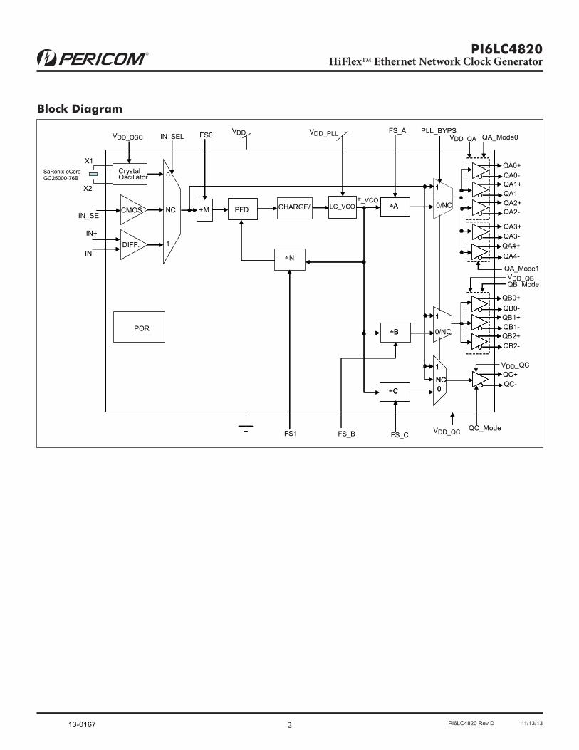
Description The PI6LC4820 is an LC VCO based low phase noise design intended for 10GbE applications. Typical 10GbE usage assumes a 25Mhz crystal input, while the PLL loop is used to generate the 156.25MHz outputs. An additional buffered crystal oscilla-tor output is provided to serve as a low noise reference for other circuitry. For Ethernet applications other than 10GbE, programmable dividers allow for simultaneous output of 312.5, 156.25, and 125MHz.
1 FS0 Input (LVCMOS)Frequency Select Pin. Use FS0=FS1=0 for all 25MHz input sources. Internal pull-down is 100K-Ohm
2 X1 Input Crystal input pin. No internal xtal load capacitance3 X2 Output Crystal output pin. No internal xtal load capacitance4 VDD_OSC Power VDD for reference oscillator5 IN_SEL Input (LVCMOS) Input mux selection pin
6 PLL_BYPS Input (LVCMOS) Optional mode to bypass PLL and have input reference source connect directly to outputs
7 GND Power Ground pin
8 FS1 Input (LVCMOS) Frequency Select Pin. Use FS0=FS1=0 for all 25MHz input sources. Internal pull-down is 100K-Ohm
9 QC_Mode Input (LVCMOS) Out mode control pin selects LVPECL or LVDS mode. If left floating, outputs are tri-stated
10 VDDA Power VDD for analog circuitry11 GND Power Ground pin12 VDD_PLL Power VDD for PLL. 13 GND Power Ground pin14 FS_B Input (LVCMOS) Frequency Select Pin for Bank B, Output Divider15 GND Power Ground pin16 FS_A Input (LVCMOS) Frequency Select Pin for Bank A, Output Divider17 GND Power Ground pin18 FS_C Input (LVCMOS) Frequency Select Pin for Bank C, Output Divider
19 QA_Mode1 Input (LVCMOS) Out mode control pin selects LVPECL or LVDS mode. If left floating, outputs are tri-stated
20 VDD Power VDD
21 GND Power Ground pin22,23
QC-,QC+
Output (Differential) Bank C LVDS/LVPECL selectable output. Controlled by QC_Mode pin
24 VDD_QC Power VDD for bank C outputs25 VDD_QA Power VDD for bank A outputs26,27
QA4-,QA4+
Output (Differential) Bank A LVDS/LVPECL selectable output. Controlled by QA_Mode1 pin
28,29
QA3-,QA3+
Output (Differential) Bank A LVDS/LVPECL selectable output. Controlled by QA_Mode1 pin
30,31
QA2-, QA2+
Output (Differential) Bank A LVDS/LVPECL selectable output. Controlled by QA_Mode0 pin
VDD General Power Supply Voltage 3.0 3.6 V TA Ambient Temperature –40 85 °CIDD Power Supply Current All outputs loaded 425
mAIDD_A Power Supply Current for pin10 13IDD_PLL Power Supply Current for pin12 30VDDA Analog Power Supply Voltage 2.7 3.6
VVDD_PLL PLL Power Supply Voltage 2.7 3.6
LVCMOS Input Electrical Characteristics
Symbol Parameters Conditions Min. Typ. Max. Units
VIH Input High VoltageFS0, FS1
2 VVIL Input Low Voltage 0.8 VVIH Input High Current IN_SEL, PLL_BYPS,
FS_A, FS_B, FS_C, QA_Mode, QB_Mode, QC_Mode
2.6 V
VIL Input Low Current 0.8 V
IIH Input High Current VIN = VDD 45 mAIIL Input Low Current VIN = 0V -45 mARpu Internal pull up resistance 100 KWRdn Internal pull down resistance 100 KW
TDC Input Duty Cycle 35 65 %
CIN Input Capacitance1 1.5 pFFIN Input Frequency 15 160 MHz
Note:
1. There is no internal load capacitance built in to the X1 and X2 pins
Storage Temperature .......................................................... –65°C to +150°CSupply Voltage to Ground Potential, VDD ......................–0.5V to +4.6VESD Protection (HBM) ..................................................................... 2000 V
Note: Stresses greater than those listed under MAXIMUM RATINGS may cause permanent damage to the device. This is a stress rating only and functional operation of the device at these or any other conditions above those indicated in the operational sections of this specification is not implied. Exposure to absolute maximum rating conditions for extended periods may affect reliability.
Maximum Ratings(Above which useful life may be impaired. For user guidelines, not tested.)
PI6LC4820 is a high performance and low jitter clock generator for advanced Gigabit Ethernet systems. It has three independent banks whose outputs can be set to LVPECL or LVDS and in 3 outputs frequencies : 125MHz, 156.25MHz, and 312.5MHz. It is criti-cal to ensure the power supply is properly decoupled and the layout around the crystal is properly routed to achieve this low jitter performance. The following guide is highly recommended to be adopted into the system PCB designs.
1) It is suggested to use the schematic’s decoupling RC value to get best board noise filtering2) Typical LVPECL is using 150W pull down in AC or DC coupling drive according to ASIC ref_clk I/O spec3) The crystal circuit C1/C2 load values are for CL=18pF crystal, they can be adjusted for other CL crystals4) Please refer to the datasheet for other static I/O logic set for the request work modes and output frequencies
4 Copyright Pericom Semiconductor 2007 Last SlidePERICOM CONFIDENTIAL INFORMATION
2. PI6LC4820 Crystal Circuit Layout Guide
1 432 5 6 7 8
1 2 3 4 5 6 7 8
Pin name
1 FS0
2 X1
3 X2
4 VDD_OSC
5 IN_SEL
6 PLL-BYBS
7 GND
8 FS1PCB Layers:
L_1 Signal (Top)
L_2 GND plane
Solder padBoard via
keep out area
GND Pad
Crystal pad
C1 cap. padGND via
Crystal Circuit Oscillator
Crystal circuit connectionThe following diagram shows PI6LC4820 crystal circuit connection with a parallel crystal. For the CL=18pF crystal, it is suggested to use C1=27pF, C2=33pF. C1 and C2 can be adjusted to fine tune to the target ppm of crystal oscillator according to different board layouts.
C127pF
Crystal(CL=18pF)
C233pF
X1
X2
SaRonix-eCeraGC2500076B
Crystal Oscillator Circuit
Recommended Crystal Specification
Pericom recommends:
a) GC2500003 XTAL 49S/SMD(4.0 mm), 25M, CL=18pF, +/-30ppm, http://www.pericom.com/pdf/datasheets/se/GC_GF.pdf
b) FY2500081, SMD 5x3.2(4P), 25M, CL=18pF, +/-30ppm, http://www.pericom.com/pdf/datasheets/se/FY_F9.pdf
c) FL2500047, SMD 3.2x2.5(4P), 25M, CL=18pF, +/-20ppm, http://www.pericom.com/pdf/datasheets/se/FL.pdf
6 Copyright Pericom Semiconductor 2007 Last SlidePERICOM CONFIDENTIAL INFORMATION
2. PI6LC4820 Crystal Circuit Layout Guide
1 432 5 6 7 8
1 2 3 4 5 6 7 8
Pin name
1 FS0
2 X1
3 X2
4 VDD_OSC
5 IN_SEL
6 PLL-BYBS
7 GND
8 FS1PCB Layers:
L_1 Signal (Top)
L_2 GND plane
Solder padBoard via
keep out area
GND Pad
Crystal pad
C1 cap. padGND via
GND via trace L_1
4. VDD and GND Pins Layout
1) Small value decoupling caps. (0.1uF, 1uF, and 2.2uF) should be placed close to each VDD pin or via 2) Each GND pin should have its own via to the common GND plane 3) Thermal pad must be connected to the GND plane for better thermal distribution and signal conducting with reasonable via counts (>6)
5. LVPECL Differential Output Layout
1) 150W pull-down should be put close to clock output side with symmetrical position in one pair 2) Do not share 150W pull-down GND via between each pairs
6. Differential Input
1) This device differential input (pin 47, 48) can accept 25MHz, 125MHz, and 156.25MHz frequencies in most common differential signals (LVPECL, LVDS, HCSL etc.) in either AC or DC coupling, with proper IN_SEL, FS0, and FS1 setting2) The device differential input has equivalent 100W differential termination on chip, so PCB 100W external termination is normally not necessary.
Crystal Layout Example
1) X1 pin is the most sensitive as crystal amplifier input2) X1 and X2 pins connected to crystal trace loop should be very narrow without any board via in the loop and keep the via out of the area3) Place crystal as close to the IC as possible along with C1/C2 load caps. There should be no via at the top layer to the crystal4) Keep crystal load cap. C1/C2 to GND sides as close as possible so that the minimum board noise could be coupled into the caps
Notes:1. All dimensions are in millimeters, angles are in degrees.2. Refer JEDEC MO-220/VKKD3. Thermal Pad Soldering Area4. Depending on the method of lead termination at the edge of the package, pull back maybe present.
DATE: 0543/09/12
12-0458
Note:
1. • For latest package info, please check: http://www.pericom.com/products/packaging/mechanicals.php