1. General description The PCA9552 LED blinker blinks LEDs in I 2 C-bus and SMBus applications where it is necessary to limit bus traffic or free up the I 2 C-bus master's (MCU, MPU, DSP, chip set, etc.) timer. The uniqueness of this device is the internal oscillator with two programmable blink rates. To blink LEDs using normal I/O expanders like the PCF8574 or PCA9554, the bus master must send repeated commands to turn the LED on and off. This greatly increases the amount of traffic on the I 2 C-bus and uses up one of the master's timers. The PCA9552 LED blinker instead requires only the initial setup command to program BLINK RATE 1 and BLINK RATE 2 (that is, the frequency and duty cycle) for each individual output. From then on, only one command from the bus master is required to turn each individual open-drain output on, off, or to cycle at BLINK RATE 1 or BLINK RATE 2. Maximum output sink current is 25 mA per bit and 200 mA per package. Any bits not used for controlling the LEDs can be used for General Purpose Parallel Input/Output (GPIO) expansion. The active LOW hardware reset pin ( RESET) and Power-On Reset (POR) initializes the registers to their default state, all zeroes, causing the bits to be set HIGH (LED off). Three hardware address pins on the PCA9552 allow eight devices to operate on the same bus. 2. Features ■ 16 LED drivers (on, off, flashing at a programmable rate) ■ 2 selectable, fully programmable blink rates (frequency and duty cycle) between 0.172 Hz and 44 Hz (5.82 seconds and 0.023 seconds) ■ Input/outputs not used as LED drivers can be used as regular GPIOs ■ Internal oscillator requires no external components ■ I 2 C-bus interface logic compatible with SMBus ■ Internal power-on reset ■ Noise filter on SCL/SDA inputs ■ Active LOW reset input ■ 16 open-drain outputs directly drive LEDs to 25 mA ■ Edge rate control on outputs ■ No glitch on power-up ■ Supports hot insertion ■ Low standby current ■ Operating power supply voltage range of 2.3 V to 5.5 V ■ 0 Hz to 400 kHz clock frequency PCA9552 16-bit I 2 C-bus LED driver with programmable blink rates Rev. 05 — 9 March 2006 Product data sheet
Transcript
1. General description
The PCA9552 LED blinker blinks LEDs in I2C-bus and SMBus applications where it isnecessary to limit bus traffic or free up the I2C-bus master's (MCU, MPU, DSP, chip set,etc.) timer. The uniqueness of this device is the internal oscillator with two programmableblink rates. To blink LEDs using normal I/O expanders like the PCF8574 or PCA9554, thebus master must send repeated commands to turn the LED on and off. This greatlyincreases the amount of traffic on the I2C-bus and uses up one of the master's timers. ThePCA9552 LED blinker instead requires only the initial setup command to programBLINK RATE 1 and BLINK RATE 2 (that is, the frequency and duty cycle) for eachindividual output. From then on, only one command from the bus master is required toturn each individual open-drain output on, off, or to cycle at BLINK RATE 1 orBLINK RATE 2. Maximum output sink current is 25 mA per bit and 200 mA per package.
Any bits not used for controlling the LEDs can be used for General Purpose ParallelInput/Output (GPIO) expansion.
The active LOW hardware reset pin (RESET) and Power-On Reset (POR) initializes theregisters to their default state, all zeroes, causing the bits to be set HIGH (LED off).
Three hardware address pins on the PCA9552 allow eight devices to operate on the samebus.
2. Features
16 LED drivers (on, off, flashing at a programmable rate)
2 selectable, fully programmable blink rates (frequency and duty cycle) between0.172 Hz and 44 Hz (5.82 seconds and 0.023 seconds)
Input/outputs not used as LED drivers can be used as regular GPIOs
Internal oscillator requires no external components
I2C-bus interface logic compatible with SMBus
Internal power-on reset
Noise filter on SCL/SDA inputs
Active LOW reset input
16 open-drain outputs directly drive LEDs to 25 mA
Edge rate control on outputs
No glitch on power-up
Supports hot insertion
Low standby current
Operating power supply voltage range of 2.3 V to 5.5 V
0 Hz to 400 kHz clock frequency
PCA955216-bit I 2C-bus LED driver with programmable blink ratesRev. 05 — 9 March 2006 Product data sheet
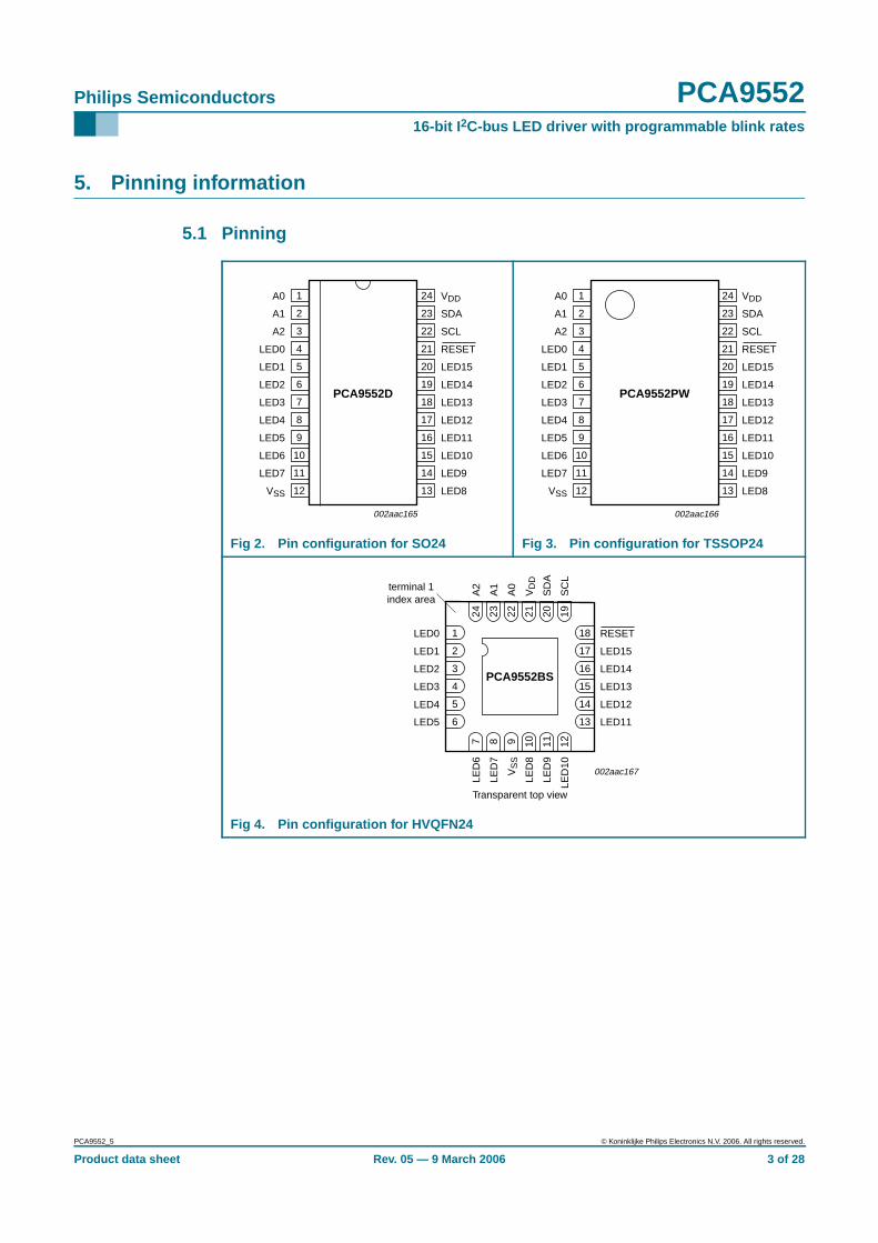
Philips Semiconductors PCA955216-bit I 2C-bus LED driver with programmable blink rates
ESD protection exceeds 2000 V HBM per JESD22-A114, 150 V MM perJESD22-A115 and 1000 V CDM per JESD22-C101
Latch-up testing is done to JEDEC Standard JESD78 which exceeds 100 mA
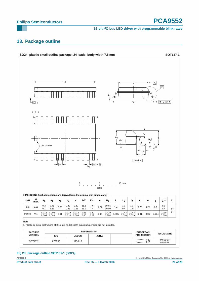
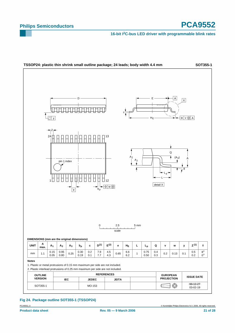
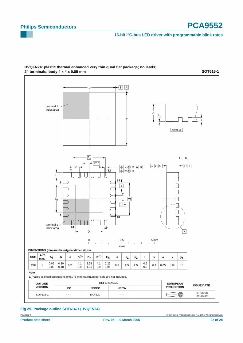
Packages offered: SO24, TSSOP24, HVQFN24
3. Ordering information
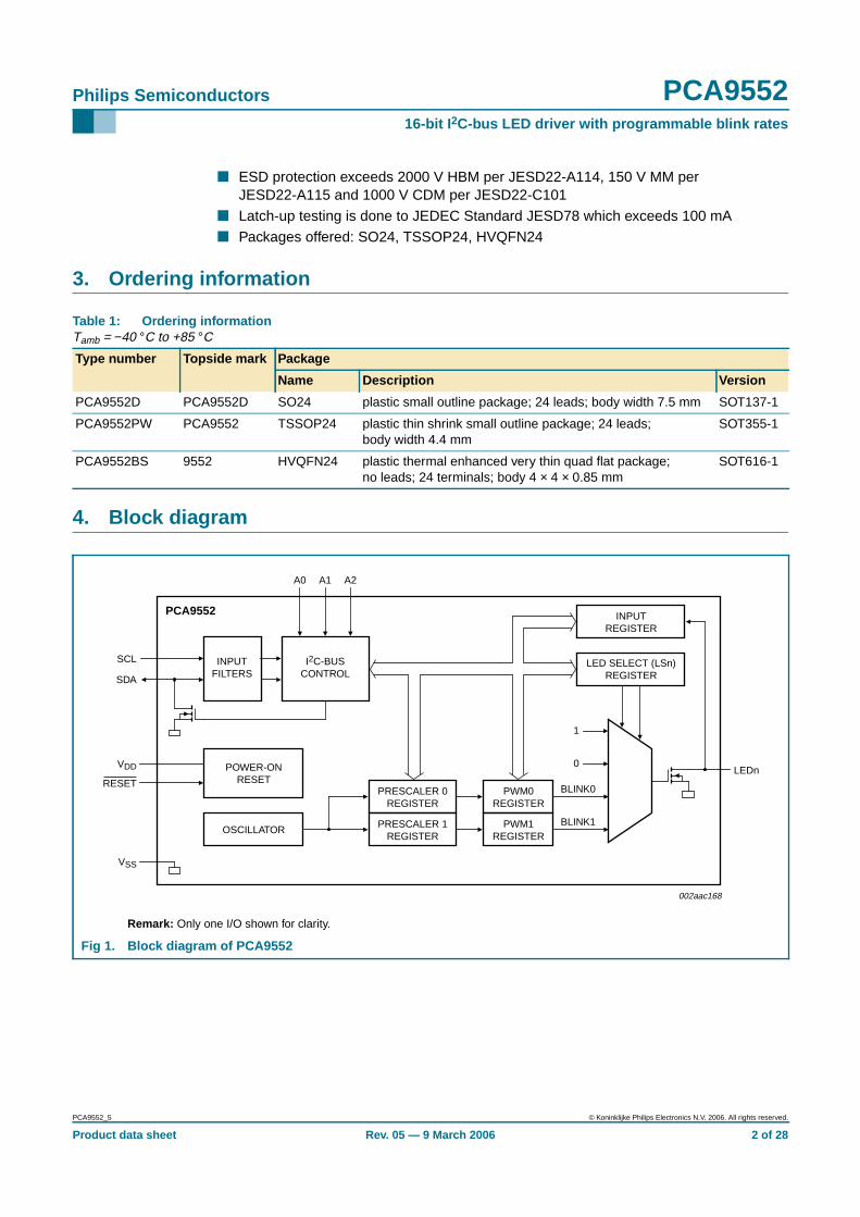
4. Block diagram
Table 1: Ordering informationTamb = −40 °C to +85 °C
Type number Topside mark Package
Name Description Version
PCA9552D PCA9552D SO24 plastic small outline package; 24 leads; body width 7.5 mm SOT137-1
PCA9552PW PCA9552 TSSOP24 plastic thin shrink small outline package; 24 leads;body width 4.4 mm
SOT355-1
PCA9552BS 9552 HVQFN24 plastic thermal enhanced very thin quad flat package;no leads; 24 terminals; body 4 × 4 × 0.85 mm
Philips Semiconductors PCA955216-bit I 2C-bus LED driver with programmable blink rates
5.2 Pin description
[1] HVQFN package die supply ground is connected to both VSS pin and exposed center pad. VSS pin must beconnected to supply ground for proper device operation. For enhanced thermal, electrical, and board levelperformance, the exposed pad needs to be soldered to the board using a corresponding thermal pad on theboard and for proper heat conduction through the board, thermal vias need to be incorporated in theprinted-circuit board in the thermal pad region.
Philips Semiconductors PCA955216-bit I 2C-bus LED driver with programmable blink rates
6. Functional description
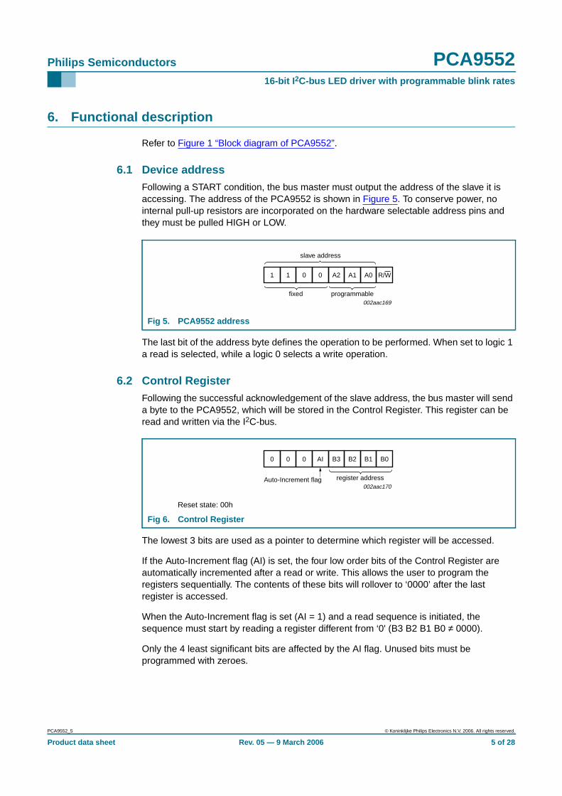
Refer to Figure 1 “Block diagram of PCA9552”.
6.1 Device addressFollowing a START condition, the bus master must output the address of the slave it isaccessing. The address of the PCA9552 is shown in Figure 5. To conserve power, nointernal pull-up resistors are incorporated on the hardware selectable address pins andthey must be pulled HIGH or LOW.
The last bit of the address byte defines the operation to be performed. When set to logic 1a read is selected, while a logic 0 selects a write operation.
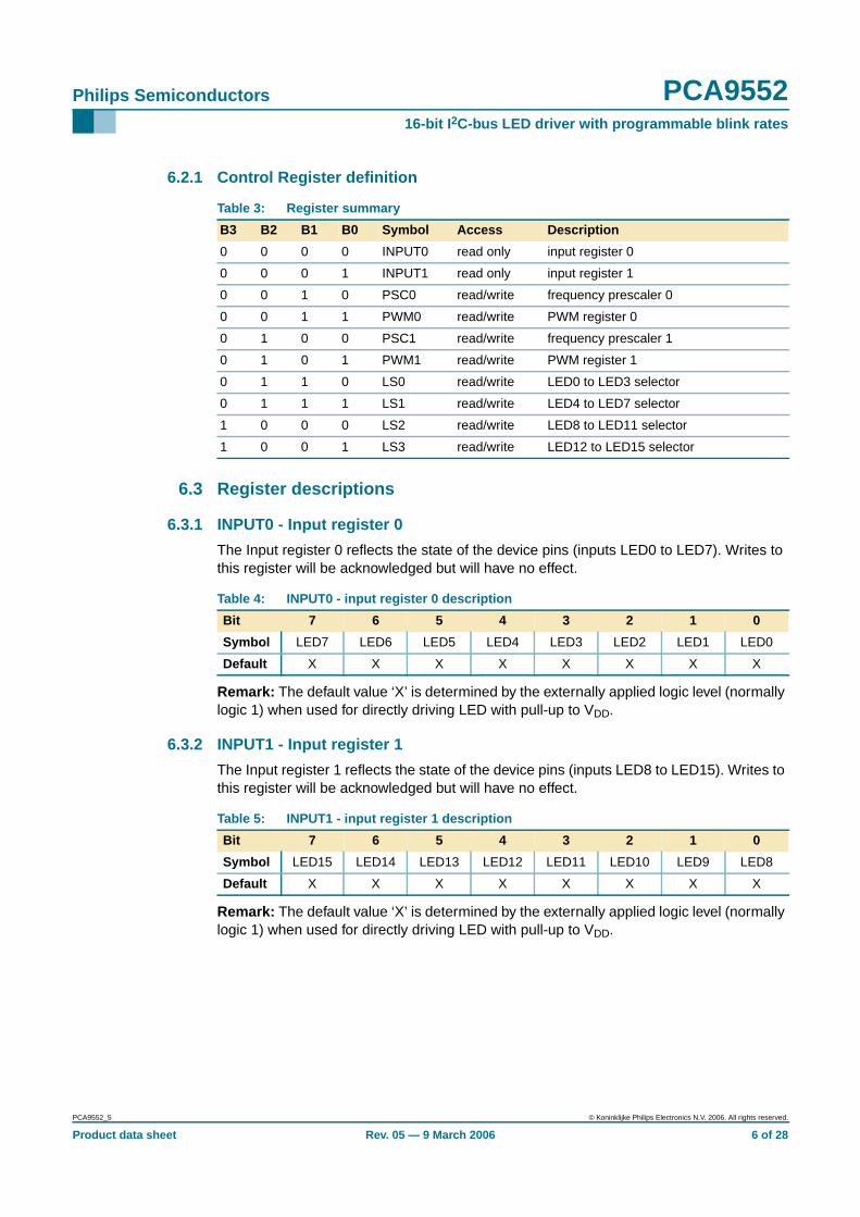
6.2 Control RegisterFollowing the successful acknowledgement of the slave address, the bus master will senda byte to the PCA9552, which will be stored in the Control Register. This register can beread and written via the I2C-bus.
The lowest 3 bits are used as a pointer to determine which register will be accessed.
If the Auto-Increment flag (AI) is set, the four low order bits of the Control Register areautomatically incremented after a read or write. This allows the user to program theregisters sequentially. The contents of these bits will rollover to ‘0000’ after the lastregister is accessed.
When the Auto-Increment flag is set (AI = 1) and a read sequence is initiated, thesequence must start by reading a register different from ‘0' (B3 B2 B1 B0 ≠ 0000).
Only the 4 least significant bits are affected by the AI flag. Unused bits must beprogrammed with zeroes.
Philips Semiconductors PCA955216-bit I 2C-bus LED driver with programmable blink rates
6.2.1 Control Register definition
6.3 Register descriptions
6.3.1 INPUT0 - Input register 0
The Input register 0 reflects the state of the device pins (inputs LED0 to LED7). Writes tothis register will be acknowledged but will have no effect.
Remark: The default value ‘X’ is determined by the externally applied logic level (normallylogic 1) when used for directly driving LED with pull-up to VDD.
6.3.2 INPUT1 - Input register 1
The Input register 1 reflects the state of the device pins (inputs LED8 to LED15). Writes tothis register will be acknowledged but will have no effect.
Remark: The default value ‘X’ is determined by the externally applied logic level (normallylogic 1) when used for directly driving LED with pull-up to VDD.
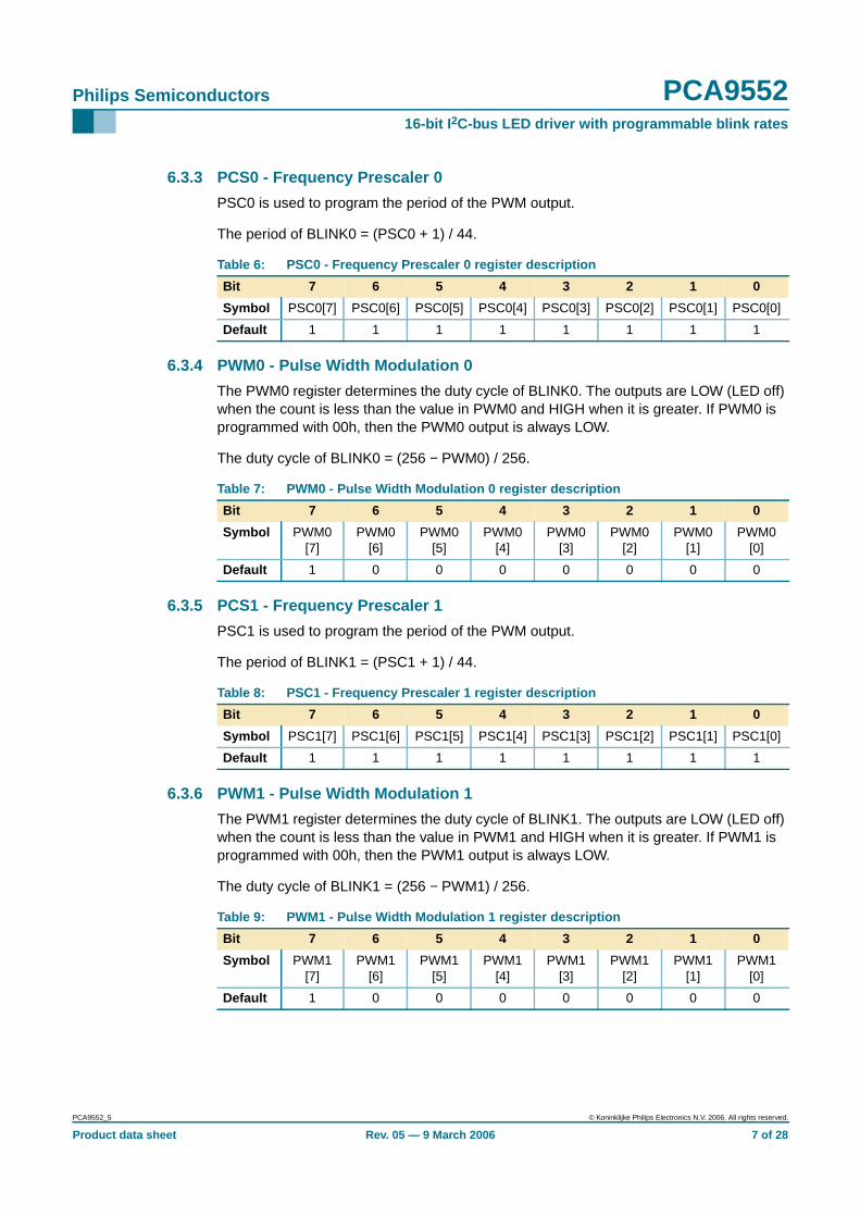
Table 3: Register summary
B3 B2 B1 B0 Symbol Access Description
0 0 0 0 INPUT0 read only input register 0
0 0 0 1 INPUT1 read only input register 1
0 0 1 0 PSC0 read/write frequency prescaler 0
0 0 1 1 PWM0 read/write PWM register 0
0 1 0 0 PSC1 read/write frequency prescaler 1
0 1 0 1 PWM1 read/write PWM register 1
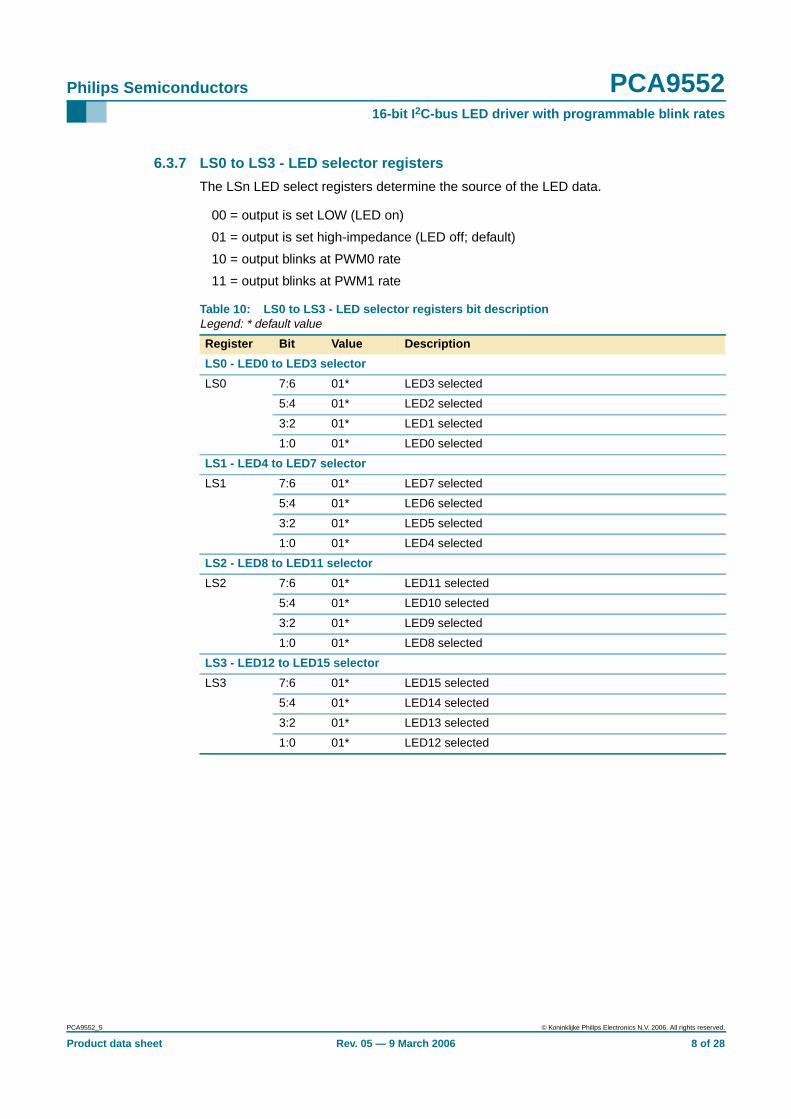
0 1 1 0 LS0 read/write LED0 to LED3 selector
0 1 1 1 LS1 read/write LED4 to LED7 selector
1 0 0 0 LS2 read/write LED8 to LED11 selector
1 0 0 1 LS3 read/write LED12 to LED15 selector
Table 4: INPUT0 - input register 0 description
Bit 7 6 5 4 3 2 1 0
Symbol LED7 LED6 LED5 LED4 LED3 LED2 LED1 LED0
Default X X X X X X X X
Table 5: INPUT1 - input register 1 description
Bit 7 6 5 4 3 2 1 0
Symbol LED15 LED14 LED13 LED12 LED11 LED10 LED9 LED8
Philips Semiconductors PCA955216-bit I 2C-bus LED driver with programmable blink rates
6.3.3 PCS0 - Frequency Prescaler 0
PSC0 is used to program the period of the PWM output.
The period of BLINK0 = (PSC0 + 1) / 44.
6.3.4 PWM0 - Pulse Width Modulation 0
The PWM0 register determines the duty cycle of BLINK0. The outputs are LOW (LED off)when the count is less than the value in PWM0 and HIGH when it is greater. If PWM0 isprogrammed with 00h, then the PWM0 output is always LOW.
The duty cycle of BLINK0 = (256 − PWM0) / 256.
6.3.5 PCS1 - Frequency Prescaler 1
PSC1 is used to program the period of the PWM output.
The period of BLINK1 = (PSC1 + 1) / 44.
6.3.6 PWM1 - Pulse Width Modulation 1
The PWM1 register determines the duty cycle of BLINK1. The outputs are LOW (LED off)when the count is less than the value in PWM1 and HIGH when it is greater. If PWM1 isprogrammed with 00h, then the PWM1 output is always LOW.
The duty cycle of BLINK1 = (256 − PWM1) / 256.
Table 6: PSC0 - Frequency Prescaler 0 register description
Bit 7 6 5 4 3 2 1 0
Symbol PSC0[7] PSC0[6] PSC0[5] PSC0[4] PSC0[3] PSC0[2] PSC0[1] PSC0[0]
Philips Semiconductors PCA955216-bit I 2C-bus LED driver with programmable blink rates
6.4 Pins used as GPIOsLED pins not used to control LEDs can be used as general purpose I/Os (GPIOs).
For use as input, set LEDn to high-impedance (01) and then read the pin state via theinput register.
For use as output, connect external pull-up resistor to the pin and size it according to theDC recommended operating characteristics. LED output pin is HIGH when the output isprogrammed as high-impedance, and LOW when the output is programmed LOW throughthe ‘LED selector’ register. The output can be pulse-width controlled when PWM0 orPWM1 are used.
6.5 Power-on resetWhen power is applied to VDD, an internal Power-On Reset (POR) holds the PCA9552 ina reset condition until VDD has reached VPOR. At that point, the reset condition is releasedand the PCA9552 registers are initialized to their default states. Thereafter, VDD must belowered below 0.2 V to reset the device.
6.6 External RESETA reset can be accomplished by holding the RESET pin LOW for a minimum of tw(rst). ThePCA9552 registers and I2C-bus state machine will be held in their default states until theRESET input is once again HIGH.
This input requires a pull-up resistor to VDD if no active connection is used.
Philips Semiconductors PCA955216-bit I 2C-bus LED driver with programmable blink rates
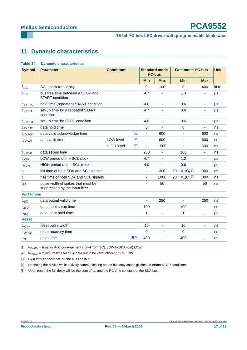
7. Characteristics of the I 2C-bus
The I2C-bus is for 2-way, 2-line communication between different ICs or modules. The twolines are a serial data line (SDA) and a serial clock line (SCL). Both lines must beconnected to a positive supply via a pull-up resistor when connected to the output stagesof a device. Data transfer may be initiated only when the bus is not busy.
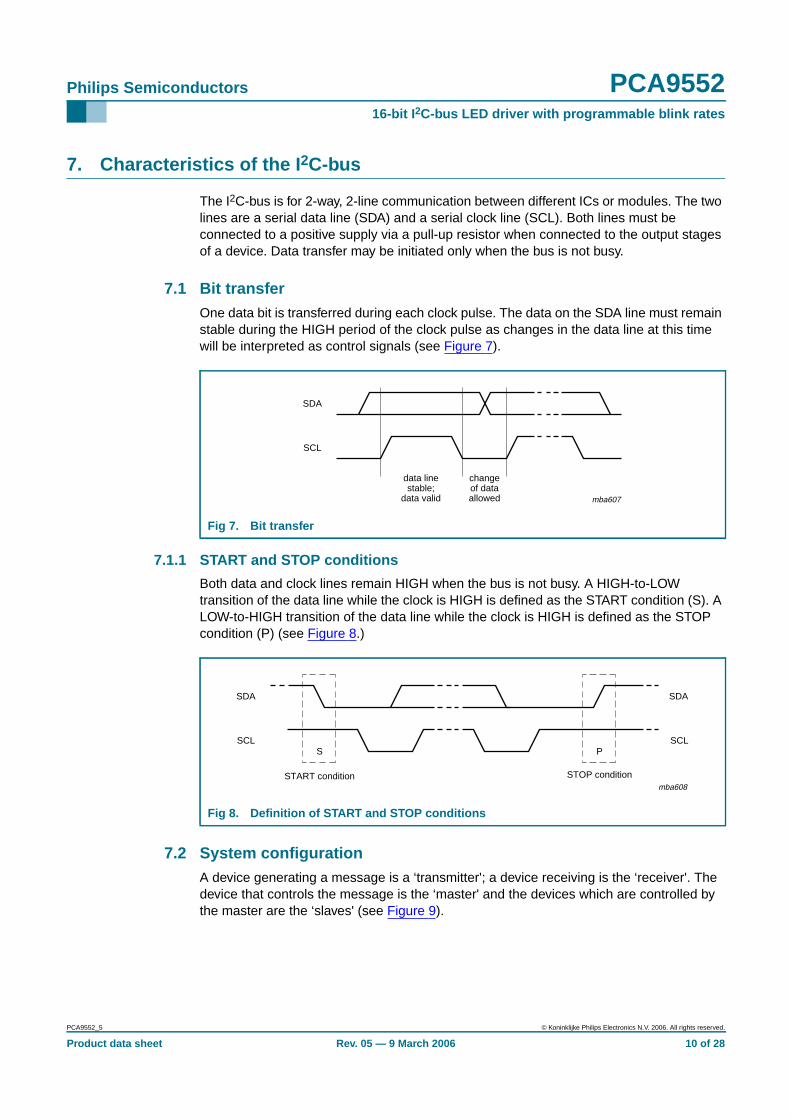
7.1 Bit transferOne data bit is transferred during each clock pulse. The data on the SDA line must remainstable during the HIGH period of the clock pulse as changes in the data line at this timewill be interpreted as control signals (see Figure 7).
7.1.1 START and STOP conditions
Both data and clock lines remain HIGH when the bus is not busy. A HIGH-to-LOWtransition of the data line while the clock is HIGH is defined as the START condition (S). ALOW-to-HIGH transition of the data line while the clock is HIGH is defined as the STOPcondition (P) (see Figure 8.)
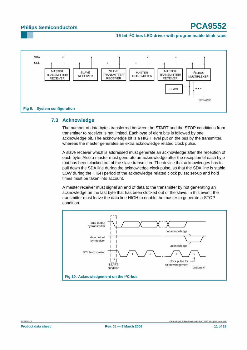
7.2 System configurationA device generating a message is a ‘transmitter'; a device receiving is the ‘receiver'. Thedevice that controls the message is the ‘master' and the devices which are controlled bythe master are the ‘slaves' (see Figure 9).
Product data sheet Rev. 05 — 9 March 2006 10 of 28
Philips Semiconductors PCA955216-bit I 2C-bus LED driver with programmable blink rates
7.3 AcknowledgeThe number of data bytes transferred between the START and the STOP conditions fromtransmitter to receiver is not limited. Each byte of eight bits is followed by oneacknowledge bit. The acknowledge bit is a HIGH level put on the bus by the transmitter,whereas the master generates an extra acknowledge related clock pulse.
A slave receiver which is addressed must generate an acknowledge after the reception ofeach byte. Also a master must generate an acknowledge after the reception of each bytethat has been clocked out of the slave transmitter. The device that acknowledges has topull down the SDA line during the acknowledge clock pulse, so that the SDA line is stableLOW during the HIGH period of the acknowledge related clock pulse; set-up and holdtimes must be taken into account.
A master receiver must signal an end of data to the transmitter by not generating anacknowledge on the last byte that has been clocked out of the slave. In this event, thetransmitter must leave the data line HIGH to enable the master to generate a STOPcondition.
Product data sheet Rev. 05 — 9 March 2006 12 of 28
Philips Semiconductors PCA955216-bit I 2C-bus LED driver with programmable blink rates
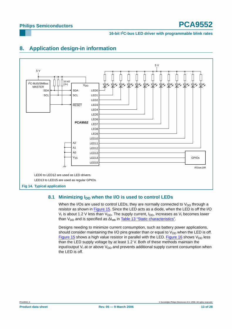
8. Application design-in information
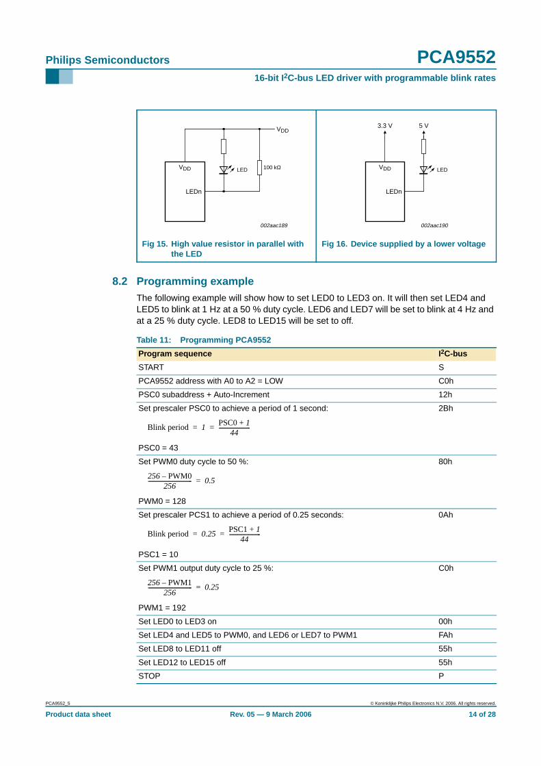
8.1 Minimizing I DD when the I/O is used to control LEDsWhen the I/Os are used to control LEDs, they are normally connected to VDD through aresistor as shown in Figure 15. Since the LED acts as a diode, when the LED is off the I/OVI is about 1.2 V less than VDD. The supply current, IDD, increases as VI becomes lowerthan VDD and is specified as ∆Istb in Table 13 “Static characteristics”.
Designs needing to minimize current consumption, such as battery power applications,should consider maintaining the I/O pins greater than or equal to VDD when the LED is off.Figure 15 shows a high value resistor in parallel with the LED. Figure 16 shows VDD lessthan the LED supply voltage by at least 1.2 V. Both of these methods maintain theinput/output VI at or above VDD and prevents additional supply current consumption whenthe LED is off.
Product data sheet Rev. 05 — 9 March 2006 13 of 28
Philips Semiconductors PCA955216-bit I 2C-bus LED driver with programmable blink rates
8.2 Programming exampleThe following example will show how to set LED0 to LED3 on. It will then set LED4 andLED5 to blink at 1 Hz at a 50 % duty cycle. LED6 and LED7 will be set to blink at 4 Hz andat a 25 % duty cycle. LED8 to LED15 will be set to off.
Fig 15. High value resistor in parallel withthe LED
Fig 16. Device supplied by a lower voltage
002aac189
LEDVDD
LEDn
100 kΩ
VDD
002aac190
LEDVDD
LEDn
3.3 V 5 V
Table 11: Programming PCA9552
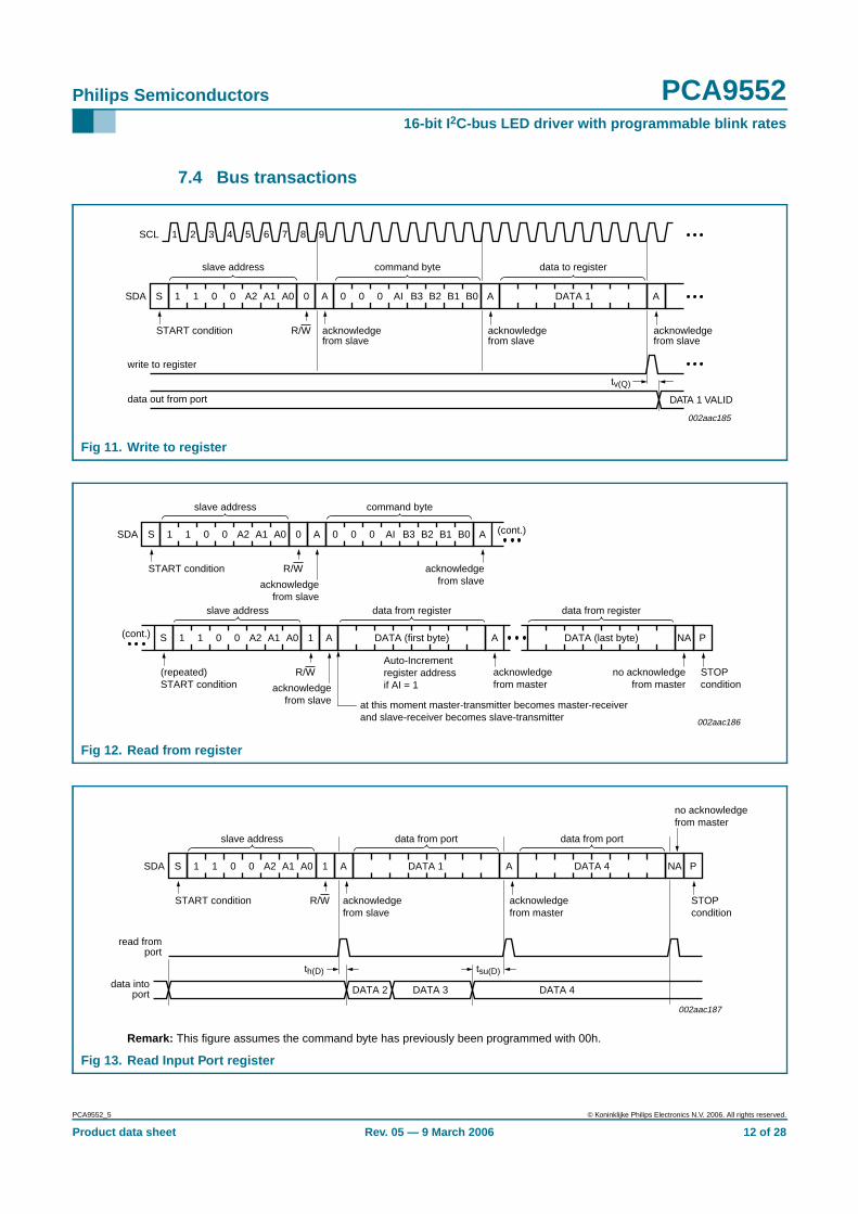
Program sequence I2C-bus
START S
PCA9552 address with A0 to A2 = LOW C0h
PSC0 subaddress + Auto-Increment 12h
Set prescaler PSC0 to achieve a period of 1 second:
PSC0 = 43
2Bh
Set PWM0 duty cycle to 50 %:
PWM0 = 128
80h
Set prescaler PCS1 to achieve a period of 0.25 seconds:
PSC1 = 10
0Ah
Set PWM1 output duty cycle to 25 %:
PWM1 = 192
C0h
Set LED0 to LED3 on 00h
Set LED4 and LED5 to PWM0, and LED6 or LED7 to PWM1 FAh
Product data sheet Rev. 05 — 9 March 2006 15 of 28
Philips Semiconductors PCA955216-bit I 2C-bus LED driver with programmable blink rates
[1] All typical values at 3.3 V and 25 °C.
[2] VDD must be lowered to 0.2 V in order to reset part.
[3] Each I/O must be externally limited to a maximum of 25 mA and each octal ([LED0 to LED7] and [LED8 to LED15]) must be limited to amaximum current of 100 mA for a device total of 200 mA.
Select inputs A0, A1, A2; RESET
VIL LOW-level input voltage −0.5 - 0.8 V
VIH HIGH-level input voltage 2.0 - 5.5 V
ILI input leakage current −1 - +1 µA
Ci input capacitance VI = VSS - 2.3 5 pF
Table 13: Static characteristics …continuedVDD = 2.3 V to 5.5 V; VSS = 0 V; Tamb = −40 °C to +85 °C; unless otherwise specified.
Symbol Parameter Conditions Min Typ [1] Max Unit
(1) maximum
(2) average
(3) minimum
(1) maximum
(2) average
(3) minimum
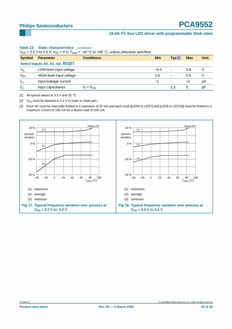
Fig 17. Typical frequency variation over process atVDD = 2.3 V to 3.0 V
Fig 18. Typical frequency variation over process atVDD = 3.0 V to 5.5 V
Product data sheet Rev. 05 — 9 March 2006 22 of 28
Philips Semiconductors PCA955216-bit I 2C-bus LED driver with programmable blink rates
14. Handling information
Inputs and outputs are protected against electrostatic discharge in normal handling.However, to be completely safe you must take normal precautions appropriate to handlingintegrated circuits.
15. Soldering
15.1 Introduction to soldering surface mount packagesThis text gives a very brief insight to a complex technology. A more in-depth account ofsoldering ICs can be found in our Data Handbook IC26; Integrated Circuit Packages(document order number 9398 652 90011).
There is no soldering method that is ideal for all surface mount IC packages. Wavesoldering can still be used for certain surface mount ICs, but it is not suitable for fine pitchSMDs. In these situations reflow soldering is recommended.
15.2 Reflow solderingReflow soldering requires solder paste (a suspension of fine solder particles, flux andbinding agent) to be applied to the printed-circuit board by screen printing, stencilling orpressure-syringe dispensing before package placement. Driven by legislation andenvironmental forces the worldwide use of lead-free solder pastes is increasing.
Several methods exist for reflowing; for example, convection or convection/infraredheating in a conveyor type oven. Throughput times (preheating, soldering and cooling)vary between 100 seconds and 200 seconds depending on heating method.
Typical reflow peak temperatures range from 215 °C to 270 °C depending on solder pastematerial. The top-surface temperature of the packages should preferably be kept:
• below 225 °C (SnPb process) or below 245 °C (Pb-free process)
– for all BGA, HTSSON..T and SSOP..T packages
– for packages with a thickness ≥ 2.5 mm
– for packages with a thickness < 2.5 mm and a volume ≥ 350 mm3 so calledthick/large packages.
• below 240 °C (SnPb process) or below 260 °C (Pb-free process) for packages with athickness < 2.5 mm and a volume < 350 mm3 so called small/thin packages.
Moisture sensitivity precautions, as indicated on packing, must be respected at all times.
15.3 Wave solderingConventional single wave soldering is not recommended for surface mount devices(SMDs) or printed-circuit boards with a high component density, as solder bridging andnon-wetting can present major problems.
To overcome these problems the double-wave soldering method was specificallydeveloped.
If wave soldering is used the following conditions must be observed for optimal results:
Product data sheet Rev. 05 — 9 March 2006 23 of 28
Philips Semiconductors PCA955216-bit I 2C-bus LED driver with programmable blink rates
• Use a double-wave soldering method comprising a turbulent wave with high upwardpressure followed by a smooth laminar wave.
• For packages with leads on two sides and a pitch (e):
– larger than or equal to 1.27 mm, the footprint longitudinal axis is preferred to beparallel to the transport direction of the printed-circuit board;
– smaller than 1.27 mm, the footprint longitudinal axis must be parallel to thetransport direction of the printed-circuit board.
The footprint must incorporate solder thieves at the downstream end.
• For packages with leads on four sides, the footprint must be placed at a 45° angle tothe transport direction of the printed-circuit board. The footprint must incorporatesolder thieves downstream and at the side corners.
During placement and before soldering, the package must be fixed with a droplet ofadhesive. The adhesive can be applied by screen printing, pin transfer or syringedispensing. The package can be soldered after the adhesive is cured.
Typical dwell time of the leads in the wave ranges from 3 seconds to 4 seconds at 250 °Cor 265 °C, depending on solder material applied, SnPb or Pb-free respectively.
A mildly-activated flux will eliminate the need for removal of corrosive residues in mostapplications.
15.4 Manual solderingFix the component by first soldering two diagonally-opposite end leads. Use a low voltage(24 V or less) soldering iron applied to the flat part of the lead. Contact time must belimited to 10 seconds at up to 300 °C.
When using a dedicated tool, all other leads can be soldered in one operation within2 seconds to 5 seconds between 270 °C and 320 °C.
15.5 Package related soldering information
[1] For more detailed information on the BGA packages refer to the (LF)BGA Application Note (AN01026);order a copy from your Philips Semiconductors sales office.
Table 15: Suitability of surface mount IC packages for wave and reflow soldering methods
Product data sheet Rev. 05 — 9 March 2006 24 of 28
Philips Semiconductors PCA955216-bit I 2C-bus LED driver with programmable blink rates
[2] All surface mount (SMD) packages are moisture sensitive. Depending upon the moisture content, themaximum temperature (with respect to time) and body size of the package, there is a risk that internal orexternal package cracks may occur due to vaporization of the moisture in them (the so called popcorneffect). For details, refer to the Drypack information in the Data Handbook IC26; Integrated CircuitPackages; Section: Packing Methods.
[3] These transparent plastic packages are extremely sensitive to reflow soldering conditions and must on noaccount be processed through more than one soldering cycle or subjected to infrared reflow soldering withpeak temperature exceeding 217 °C ± 10 °C measured in the atmosphere of the reflow oven. The packagebody peak temperature must be kept as low as possible.
[4] These packages are not suitable for wave soldering. On versions with the heatsink on the bottom side, thesolder cannot penetrate between the printed-circuit board and the heatsink. On versions with the heatsinkon the top side, the solder might be deposited on the heatsink surface.
[5] If wave soldering is considered, then the package must be placed at a 45° angle to the solder wavedirection. The package footprint must incorporate solder thieves downstream and at the side corners.
[6] Wave soldering is suitable for LQFP, QFP and TQFP packages with a pitch (e) larger than 0.8 mm; it isdefinitely not suitable for packages with a pitch (e) equal to or smaller than 0.65 mm.
[7] Wave soldering is suitable for SSOP, TSSOP, VSO and VSSOP packages with a pitch (e) equal to or largerthan 0.65 mm; it is definitely not suitable for packages with a pitch (e) equal to or smaller than 0.5 mm.
[8] Image sensor packages in principle should not be soldered. They are mounted in sockets or deliveredpre-mounted on flex foil. However, the image sensor package can be mounted by the client on a flex foil byusing a hot bar soldering process. The appropriate soldering profile can be provided on request.
[9] Hot bar soldering or manual soldering is suitable for PMFP packages.
Product data sheet Rev. 05 — 9 March 2006 25 of 28
Philips Semiconductors PCA955216-bit I 2C-bus LED driver with programmable blink rates
17. Revision history
Table 17: Revision history
Document ID Release date Data sheet status Change notice Doc. number Supersedes
PCA9552_5 20060309 Product data sheet - - PCA9552_4
Modifications: • The format of this data sheet has been redesigned to comply with the new presentation andinformation standard of Philips Semiconductors.
• Table 1 “Ordering information”: changed Topside mark of TSSOP24 package from‘PCA9552PW’ to ‘PCA9552’
• Section 6.6 “External RESET”: changed symbol “tW” to “tw(rst)”
• Figure 11: changed symbol “tpv” to “tv(Q)”
• Figure 13: changed symbol “tph” to “th(D)”; changed symbol “tps” to “tsu(D)”
• Section 8.1 “Minimizing IDD when the I/O is used to control LEDs”:
– 1st paragraph, 3rd sentence: changed symbol “∆IDD” to “∆Istb”
– 2nd paragraph, 4th sentence: changed symbol “VIN” to “VI”
• Table 12 “Limiting values”:
– changed parameter description of VI/O from “DC voltage on an I/O” to “voltage on aninput/output pin”
– changed symbol “II/O (DC output current on an I/O)” to ‘IO(LEDn) (output current on pin LEDn)
• Table 13 “Static characteristics”:
– moved second sentence of description below title to (new)Table note 1 and added itsreference at column “Typ”
– changed symbol “∆IDD” to “∆Istb”
– under subsection “I/Os”, changed symbol “IL” to “ILI”
• Table 14 “Dynamic characteristics”:
– updated parameter descriptions
– under subsection “Port timing”: changed symbol “tPV” to “tv(Q)”; changed symbol “tPS” to“tsu(D)”; changed symbol “tPH” to “th(D)”
– under subsection “Reset”: changed symbol “tW” to “tw(rst)”; changed symbol “tREC” to “trec(rst)”;changed symbol “tRESET” to “trst” (also in Table note 5)
• Figure 21 “Reset timing” modified to harmonize letter symbols
PCA9552_4 20041001 Product data sheet - 9397 750 13727 PCA9552_3
PCA9552_3 20030502 Product data 853-2374 29857of 2003 Apr 24
9397 750 11463 PCA9552_2
PCA9552_2 20030224 Product data 853-2374 29331of 2002 Dec 20
9397 750 11156 PCA9552_1
PCA9552_1 20020927 Product data 853-2374 28878of 2002 Sep 09
Product data sheet Rev. 05 — 9 March 2006 26 of 28
Philips Semiconductors PCA955216-bit I 2C-bus LED driver with programmable blink rates
18. Data sheet status
[1] Please consult the most recently issued data sheet before initiating or completing a design.
[2] The product status of the device(s) described in this data sheet may have changed since this data sheet was published. The latest information is available on the Internet atURL http://www.semiconductors.philips.com.
[3] For data sheets describing multiple type numbers, the highest-level product status determines the data sheet status.
19. Definitions
Short-form specification — The data in a short-form specification isextracted from a full data sheet with the same type number and title. Fordetailed information see the relevant data sheet or data handbook.
Limiting values definition — Limiting values given are in accordance withthe Absolute Maximum Rating System (IEC 60134). Stress above one ormore of the limiting values may cause permanent damage to the device.These are stress ratings only and operation of the device at these or at anyother conditions above those given in the Characteristics sections of thespecification is not implied. Exposure to limiting values for extended periodsmay affect device reliability.
Application information — Applications that are described herein for anyof these products are for illustrative purposes only. Philips Semiconductorsmake no representation or warranty that such applications will be suitable forthe specified use without further testing or modification.
20. Disclaimers
Life support — These products are not designed for use in life supportappliances, devices, or systems where malfunction of these products canreasonably be expected to result in personal injury. Philips Semiconductors
customers using or selling these products for use in such applications do soat their own risk and agree to fully indemnify Philips Semiconductors for anydamages resulting from such application.
Right to make changes — Philips Semiconductors reserves the right tomake changes in the products - including circuits, standard cells, and/orsoftware - described or contained herein in order to improve design and/orperformance. When the product is in full production (status ‘Production’),relevant changes will be communicated via a Customer Product/ProcessChange Notification (CPCN). Philips Semiconductors assumes noresponsibility or liability for the use of any of these products, conveys nolicense or title under any patent, copyright, or mask work right to theseproducts, and makes no representations or warranties that these products arefree from patent, copyright, or mask work right infringement, unless otherwisespecified.
21. Trademarks
Notice — All referenced brands, product names, service names andtrademarks are the property of their respective owners.I2C-bus — logo is a trademark of Koninklijke Philips Electronics N.V.
22. Contact information
For additional information, please visit: http://www.semiconductors.philips.com
Level Data sheet status [1] Product status [2] [3] Definition
I Objective data Development This data sheet contains data from the objective specification for product development. PhilipsSemiconductors reserves the right to change the specification in any manner without notice.
II Preliminary data Qualification This data sheet contains data from the preliminary specification. Supplementary data will be publishedat a later date. Philips Semiconductors reserves the right to change the specification without notice, inorder to improve the design and supply the best possible product.
III Product data Production This data sheet contains data from the product specification. Philips Semiconductors reserves theright to make changes at any time in order to improve the design, manufacturing and supply. Relevantchanges will be communicated via a Customer Product/Process Change Notification (CPCN).