1. General description The PCA9553 LED blinker blinks LEDs in I 2 C-bus and SMBus applications where it is necessary to limit bus traffic or free up the I 2 C-bus master's (MCU, MPU, DSP, chipset, etc.) timer. The uniqueness of this device is the internal oscillator with two programmable blink rates. To blink LEDs using normal I/O expanders like the PCF8574 or PCA9554, the bus master must send repeated commands to turn the LED on and off. This greatly increases the amount of traffic on the I 2 C-bus and uses up one of the master's timers. The PCA9553 LED blinker instead requires only the initial set-up command to program BLINK RATE 1 and BLINK RATE 2 (i.e., the frequency and duty cycle). From then on, only one command from the bus master is required to turn each individual open-drain output ON, OFF, or to cycle at BLINK RATE 1 or BLINK RATE 2. Maximum output sink current is 25 mA per bit and 100 mA per package. Any bits not used for controlling the LEDs can be used for General Purpose Parallel Input/Output (GPIO) expansion. Power-On Reset (POR) initializes the registers to their default state, all zeroes, causing the bits to be set HIGH (LED off). Due to pin limitations, the PCA9553 is not featured with hardware address pins. The PCA9553/01 and the PCA9553/02 have different fixed I 2 C-bus addresses allowing operation of both on the same bus. 2. Features ■ 4 LED drivers (on, off, flashing at a programmable rate) ■ 2 selectable, fully programmable blink rates (frequency and duty cycle) between 0.172 Hz and 44 Hz (5.82 seconds and 0.023 seconds) ■ Input/outputs not used as LED drivers can be used as regular GPIOs ■ Internal oscillator requires no external components ■ I 2 C-bus interface logic compatible with SMBus ■ Internal power-on reset ■ Noise filter on SCL/SDA inputs ■ 4 open-drain outputs directly drive LEDs to 25 mA ■ Controlled edge rates to minimize ground bounce ■ No glitch on power-up ■ Supports hot insertion ■ Low standby current ■ Operating power supply voltage range of 2.3 V to 5.5 V ■ 0 Hz to 400 kHz clock frequency PCA9553 4-bit I 2 C-bus LED driver with programmable blink rates Rev. 06 — 29 December 2008 Product data sheet
Transcript
1. General description
The PCA9553 LED blinker blinks LEDs in I2C-bus and SMBus applications where it isnecessary to limit bus traffic or free up the I2C-bus master's (MCU, MPU, DSP, chip set,etc.) timer. The uniqueness of this device is the internal oscillator with two programmableblink rates. To blink LEDs using normal I/O expanders like the PCF8574 or PCA9554, thebus master must send repeated commands to turn the LED on and off. This greatlyincreases the amount of traffic on the I2C-bus and uses up one of the master's timers. ThePCA9553 LED blinker instead requires only the initial set-up command to programBLINK RATE 1 and BLINK RATE 2 (i.e., the frequency and duty cycle). From then on, onlyone command from the bus master is required to turn each individual open-drain outputON, OFF, or to cycle at BLINK RATE 1 or BLINK RATE 2. Maximum output sink current is25 mA per bit and 100 mA per package.
Any bits not used for controlling the LEDs can be used for General Purpose ParallelInput/Output (GPIO) expansion.
Power-On Reset (POR) initializes the registers to their default state, all zeroes, causingthe bits to be set HIGH (LED off).
Due to pin limitations, the PCA9553 is not featured with hardware address pins. ThePCA9553/01 and the PCA9553/02 have different fixed I2C-bus addresses allowingoperation of both on the same bus.
2. Features
n 4 LED drivers (on, off, flashing at a programmable rate)
n 2 selectable, fully programmable blink rates (frequency and duty cycle) between0.172 Hz and 44 Hz (5.82 seconds and 0.023 seconds)
n Input/outputs not used as LED drivers can be used as regular GPIOs
n Internal oscillator requires no external components
n I2C-bus interface logic compatible with SMBus
n Internal power-on reset
n Noise filter on SCL/SDA inputs
n 4 open-drain outputs directly drive LEDs to 25 mA
n Controlled edge rates to minimize ground bounce
n No glitch on power-up
n Supports hot insertion
n Low standby current
n Operating power supply voltage range of 2.3 V to 5.5 V
n 0 Hz to 400 kHz clock frequency
PCA95534-bit I 2C-bus LED driver with programmable blink ratesRev. 06 — 29 December 2008 Product data sheet
NXP Semiconductors PCA95534-bit I 2C-bus LED driver with programmable blink rates
n ESD protection exceeds 2000 V HBM per JESD22-A114, 150 V MM perJESD22-A115 and 1000 V CDM per JESD22-C101
n Latch-up testing is done to JEDEC Standard JESD78 which exceeds 100 mA
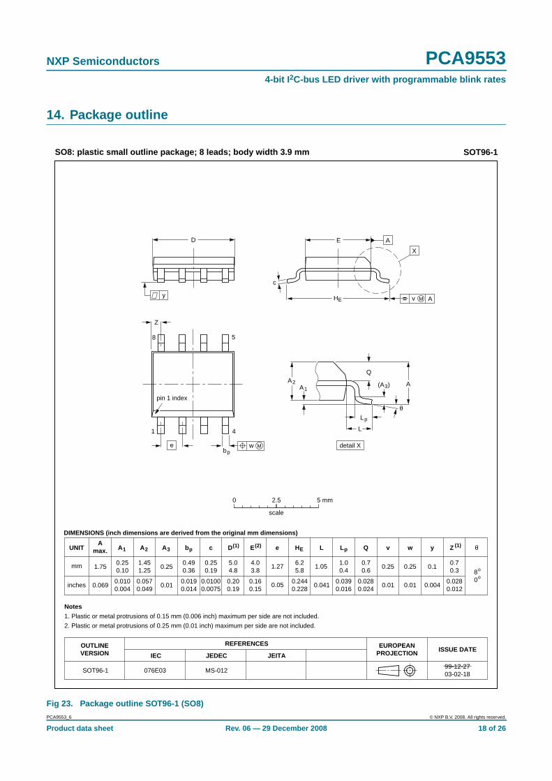
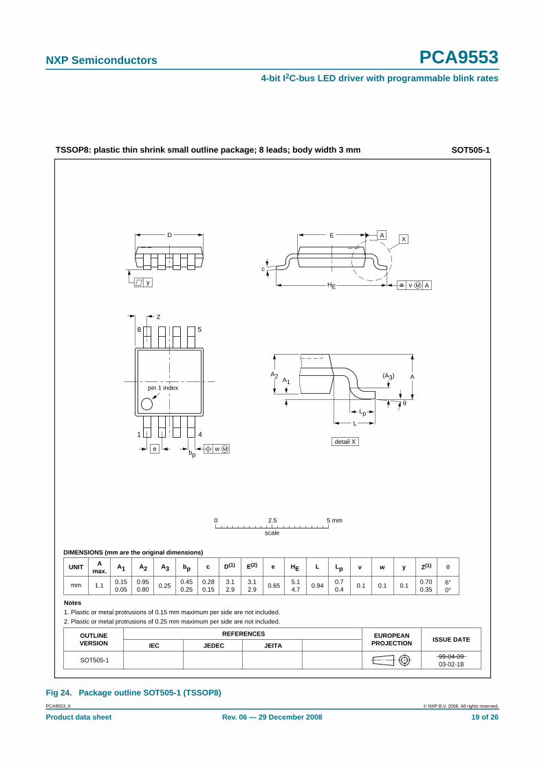
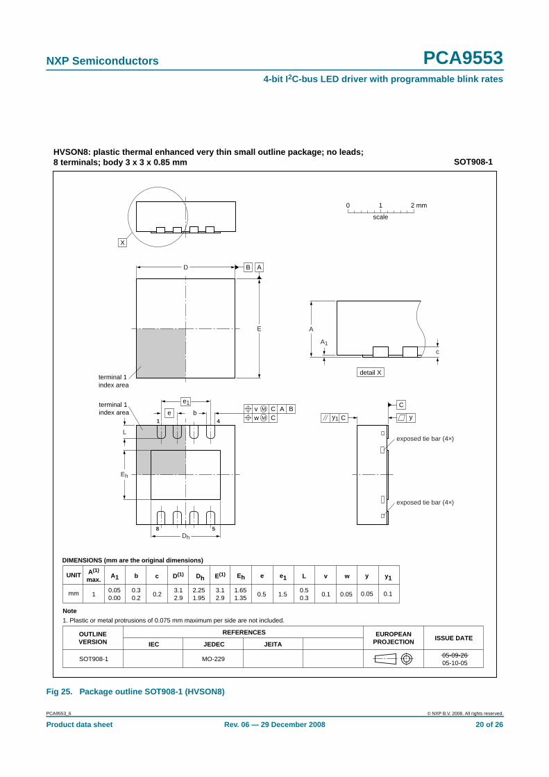
n Packages offered: SO8, TSSOP8 (MSOP8), HVSON8
3. Ordering information
[1] Also known as MSOP8.
[2] PCA9553TK uses version /01 address.
4. Marking
Table 1. Ordering information
Type number Package
Name Description Version
PCA9553D/01 SO8 plastic small outline package; 8 leads;body width 3.9 mm
SOT96-1
PCA9553D/02
PCA9553DP/01 TSSOP8[1] plastic thin shrink small outline package; 8 leads;body width 3 mm
SOT505-1
PCA9553DP/02
PCA9553TK[2] HVSON8 plastic thermal enhanced very thin small outlinepackage; no leads; 8 terminals; body 3 × 3 × 0.85 mm
Product data sheet Rev. 06 — 29 December 2008 3 of 26
NXP Semiconductors PCA95534-bit I 2C-bus LED driver with programmable blink rates
6. Pinning information
6.1 Pinning
6.2 Pin description
[1] HVSON8 package die supply ground is connected to both VSS pin and exposed center pad. VSS pin mustbe connected to supply ground for proper device operation. For enhanced thermal, electrical, and boardlevel performance, the exposed pad needs to be soldered to the board using a corresponding thermal padon the board and for proper heat conduction through the board, thermal vias need to be incorporated in thePCB in the thermal pad region.
Fig 2. Pin configuration for SO8 Fig 3. Pin configuration for TSSOP8
Product data sheet Rev. 06 — 29 December 2008 4 of 26
NXP Semiconductors PCA95534-bit I 2C-bus LED driver with programmable blink rates
7. Functional description
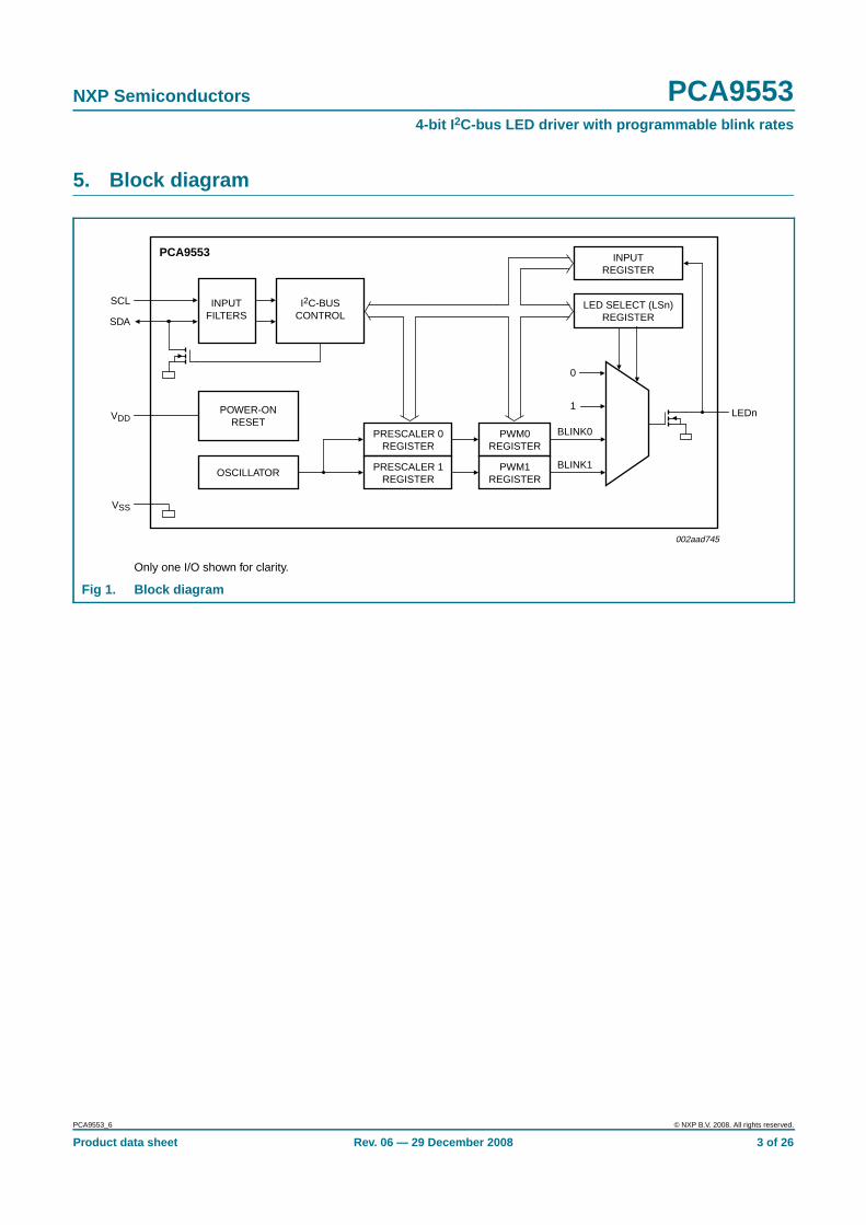
Refer to Figure 1 “Block diagram”.
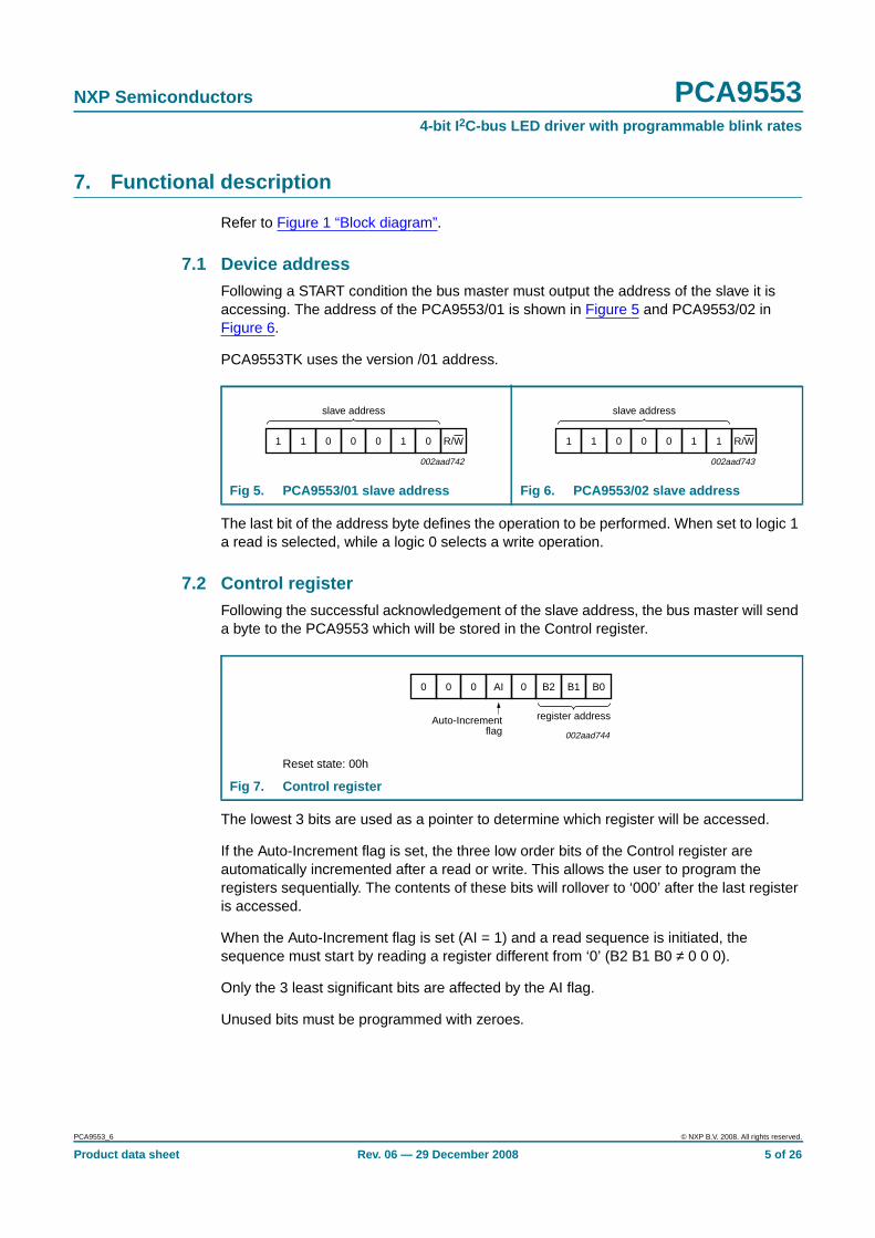
7.1 Device addressFollowing a START condition the bus master must output the address of the slave it isaccessing. The address of the PCA9553/01 is shown in Figure 5 and PCA9553/02 inFigure 6.
PCA9553TK uses the version /01 address.
The last bit of the address byte defines the operation to be performed. When set to logic 1a read is selected, while a logic 0 selects a write operation.
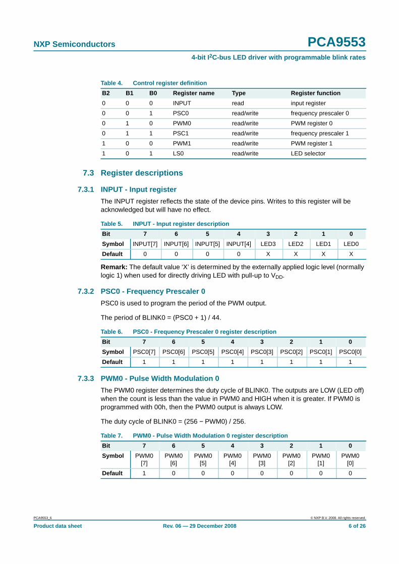
7.2 Control registerFollowing the successful acknowledgement of the slave address, the bus master will senda byte to the PCA9553 which will be stored in the Control register.
The lowest 3 bits are used as a pointer to determine which register will be accessed.
If the Auto-Increment flag is set, the three low order bits of the Control register areautomatically incremented after a read or write. This allows the user to program theregisters sequentially. The contents of these bits will rollover to ‘000’ after the last registeris accessed.
When the Auto-Increment flag is set (AI = 1) and a read sequence is initiated, thesequence must start by reading a register different from ‘0’ (B2 B1 B0 ≠ 0 0 0).
Only the 3 least significant bits are affected by the AI flag.
Product data sheet Rev. 06 — 29 December 2008 5 of 26
NXP Semiconductors PCA95534-bit I 2C-bus LED driver with programmable blink rates
7.3 Register descriptions
7.3.1 INPUT - Input register
The INPUT register reflects the state of the device pins. Writes to this register will beacknowledged but will have no effect.
Remark: The default value ‘X’ is determined by the externally applied logic level (normallylogic 1) when used for directly driving LED with pull-up to VDD.
7.3.2 PSC0 - Frequency Prescaler 0
PSC0 is used to program the period of the PWM output.
The period of BLINK0 = (PSC0 + 1) / 44.
7.3.3 PWM0 - Pulse Width Modulation 0
The PWM0 register determines the duty cycle of BLINK0. The outputs are LOW (LED off)when the count is less than the value in PWM0 and HIGH when it is greater. If PWM0 isprogrammed with 00h, then the PWM0 output is always LOW.
The duty cycle of BLINK0 = (256 − PWM0) / 256.
Table 4. Control register definition
B2 B1 B0 Register name Type Register function
0 0 0 INPUT read input register
0 0 1 PSC0 read/write frequency prescaler 0
0 1 0 PWM0 read/write PWM register 0
0 1 1 PSC1 read/write frequency prescaler 1
1 0 0 PWM1 read/write PWM register 1
1 0 1 LS0 read/write LED selector
Table 5. INPUT - Input register description
Bit 7 6 5 4 3 2 1 0
Symbol INPUT[7] INPUT[6] INPUT[5] INPUT[4] LED3 LED2 LED1 LED0
Default 0 0 0 0 X X X X
Table 6. PSC0 - Frequency Prescaler 0 register description
Bit 7 6 5 4 3 2 1 0
Symbol PSC0[7] PSC0[6] PSC0[5] PSC0[4] PSC0[3] PSC0[2] PSC0[1] PSC0[0]
Product data sheet Rev. 06 — 29 December 2008 6 of 26
NXP Semiconductors PCA95534-bit I 2C-bus LED driver with programmable blink rates
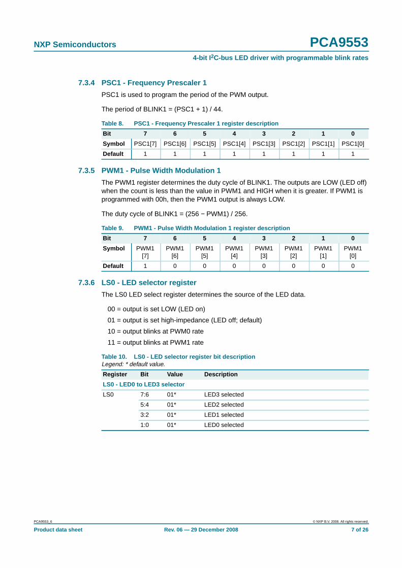
7.3.4 PSC1 - Frequency Prescaler 1
PSC1 is used to program the period of the PWM output.
The period of BLINK1 = (PSC1 + 1) / 44.
7.3.5 PWM1 - Pulse Width Modulation 1
The PWM1 register determines the duty cycle of BLINK1. The outputs are LOW (LED off)when the count is less than the value in PWM1 and HIGH when it is greater. If PWM1 isprogrammed with 00h, then the PWM1 output is always LOW.
The duty cycle of BLINK1 = (256 − PWM1) / 256.
7.3.6 LS0 - LED selector register
The LS0 LED select register determines the source of the LED data.
00 = output is set LOW (LED on)
01 = output is set high-impedance (LED off; default)
10 = output blinks at PWM0 rate
11 = output blinks at PWM1 rate
Table 8. PSC1 - Frequency Prescaler 1 register description
Bit 7 6 5 4 3 2 1 0
Symbol PSC1[7] PSC1[6] PSC1[5] PSC1[4] PSC1[3] PSC1[2] PSC1[1] PSC1[0]
Product data sheet Rev. 06 — 29 December 2008 7 of 26
NXP Semiconductors PCA95534-bit I 2C-bus LED driver with programmable blink rates
7.4 Pins used as general purpose I/OsLED pins not used to control LEDs can be used as general purpose I/Os.
For use as input: Set LEDn to high-impedance (01) and then read the pin state via theInput register.
For use as output: Connect external pull-up resistor to the pin and size it according to theDC recommended operating characteristics. LED output pin is HIGH when the output isprogrammed as high-impedance, and LOW when the output is programmed LOW throughthe ‘LED selector’ register. The output can be pulse-width controlled when PWM0 orPWM1 are used.
7.5 Power-on resetWhen power is applied to VDD, an internal Power-On Reset (POR) holds the PCA9553 ina reset condition until VDD has reached VPOR. At that point, the reset condition is releasedand the PCA9553 registers are initialized to their default states, with all outputs in the OFFstate. Thereafter, VDD must be lowered below 0.2 V to reset the device.
8. Characteristics of the I 2C-bus
The I2C-bus is for 2-way, 2-line communication between different ICs or modules. The twolines are a serial data line (SDA) and a serial clock line (SCL). Both lines must beconnected to a positive supply via a pull-up resistor when connected to the output stagesof a device. Data transfer may be initiated only when the bus is not busy.
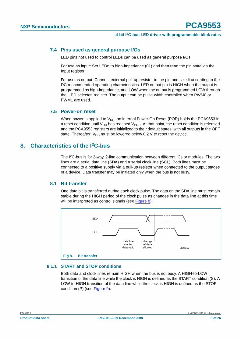
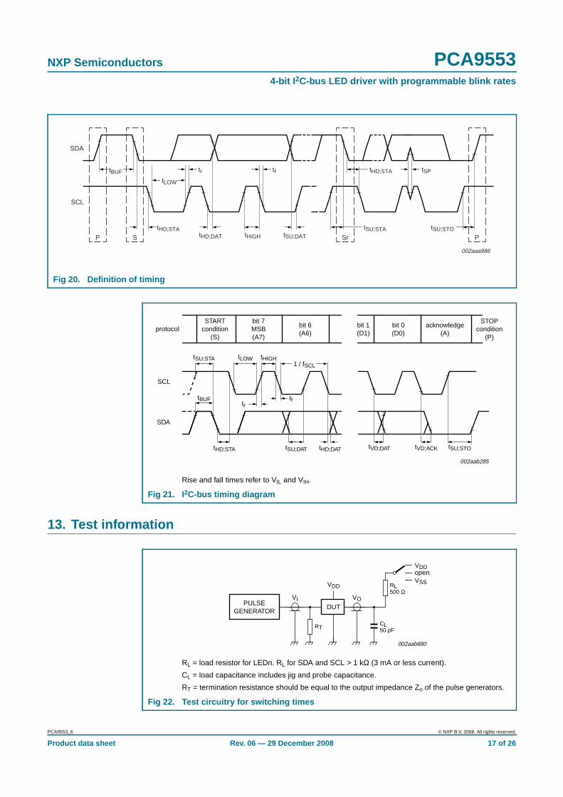
8.1 Bit transferOne data bit is transferred during each clock pulse. The data on the SDA line must remainstable during the HIGH period of the clock pulse as changes in the data line at this timewill be interpreted as control signals (see Figure 8).
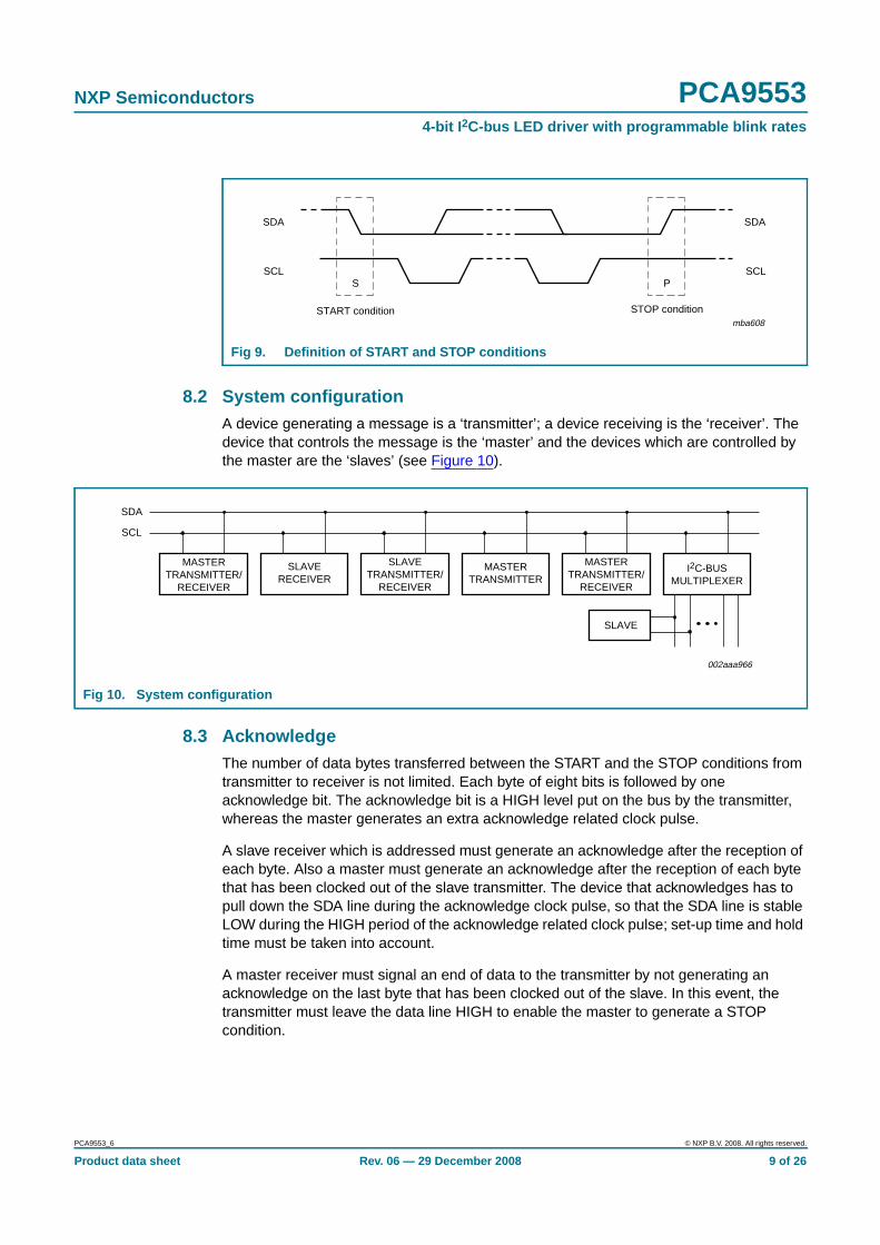
8.1.1 START and STOP conditions
Both data and clock lines remain HIGH when the bus is not busy. A HIGH-to-LOWtransition of the data line while the clock is HIGH is defined as the START condition (S). ALOW-to-HIGH transition of the data line while the clock is HIGH is defined as the STOPcondition (P) (see Figure 9).
Product data sheet Rev. 06 — 29 December 2008 8 of 26
NXP Semiconductors PCA95534-bit I 2C-bus LED driver with programmable blink rates
8.2 System configurationA device generating a message is a ‘transmitter’; a device receiving is the ‘receiver’. Thedevice that controls the message is the ‘master’ and the devices which are controlled bythe master are the ‘slaves’ (see Figure 10).
8.3 AcknowledgeThe number of data bytes transferred between the START and the STOP conditions fromtransmitter to receiver is not limited. Each byte of eight bits is followed by oneacknowledge bit. The acknowledge bit is a HIGH level put on the bus by the transmitter,whereas the master generates an extra acknowledge related clock pulse.
A slave receiver which is addressed must generate an acknowledge after the reception ofeach byte. Also a master must generate an acknowledge after the reception of each bytethat has been clocked out of the slave transmitter. The device that acknowledges has topull down the SDA line during the acknowledge clock pulse, so that the SDA line is stableLOW during the HIGH period of the acknowledge related clock pulse; set-up time and holdtime must be taken into account.
A master receiver must signal an end of data to the transmitter by not generating anacknowledge on the last byte that has been clocked out of the slave. In this event, thetransmitter must leave the data line HIGH to enable the master to generate a STOPcondition.
Product data sheet Rev. 06 — 29 December 2008 10 of 26
NXP Semiconductors PCA95534-bit I 2C-bus LED driver with programmable blink rates
9. Application design-in information
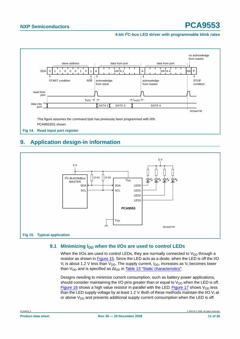
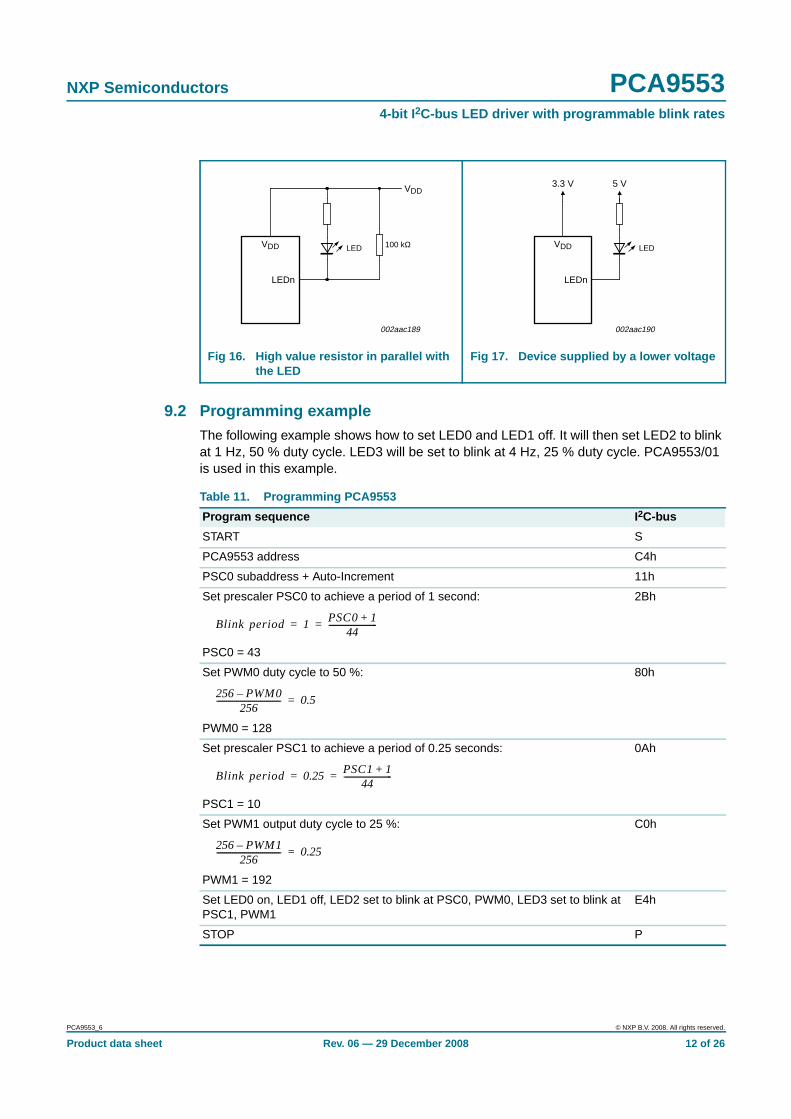
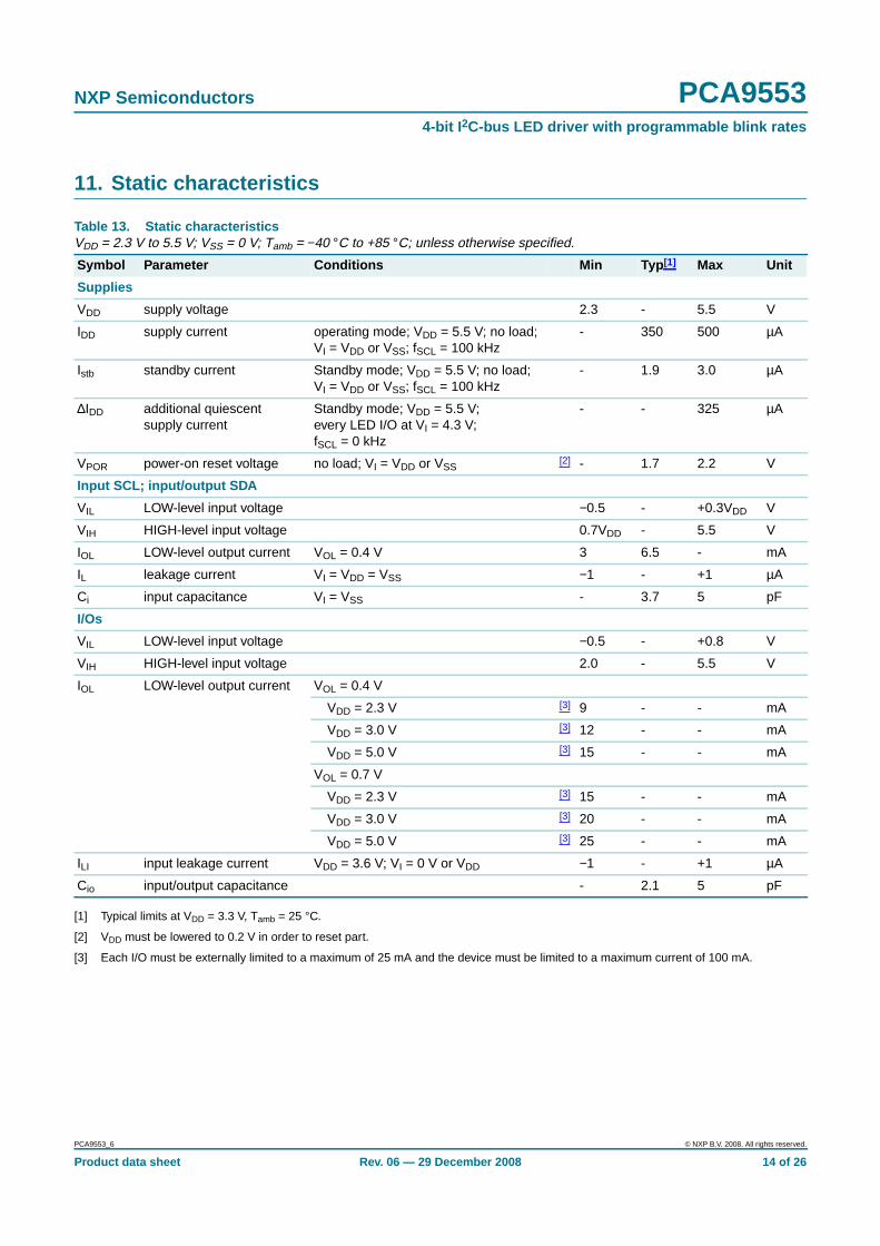
9.1 Minimizing I DD when the I/Os are used to control LEDsWhen the I/Os are used to control LEDs, they are normally connected to VDD through aresistor as shown in Figure 15. Since the LED acts as a diode, when the LED is off the I/OVI is about 1.2 V less than VDD. The supply current, IDD, increases as VI becomes lowerthan VDD and is specified as ∆IDD in Table 13 “Static characteristics”.
Designs needing to minimize current consumption, such as battery power applications,should consider maintaining the I/O pins greater than or equal to VDD when the LED is off.Figure 16 shows a high value resistor in parallel with the LED. Figure 17 shows VDD lessthan the LED supply voltage by at least 1.2 V. Both of these methods maintain the I/O VI ator above VDD and prevents additional supply current consumption when the LED is off.
This figure assumes the command byte has previously been programmed with 00h.
Product data sheet Rev. 06 — 29 December 2008 11 of 26
NXP Semiconductors PCA95534-bit I 2C-bus LED driver with programmable blink rates
9.2 Programming exampleThe following example shows how to set LED0 and LED1 off. It will then set LED2 to blinkat 1 Hz, 50 % duty cycle. LED3 will be set to blink at 4 Hz, 25 % duty cycle. PCA9553/01is used in this example.
Fig 16. High value resistor in parallel withthe LED
Fig 17. Device supplied by a lower voltage
002aac189
LEDVDD
LEDn
100 kΩ
VDD
002aac190
LEDVDD
LEDn
3.3 V 5 V
Table 11. Programming PCA9553
Program sequence I2C-bus
START S
PCA9553 address C4h
PSC0 subaddress + Auto-Increment 11h
Set prescaler PSC0 to achieve a period of 1 second:
PSC0 = 43
2Bh
Set PWM0 duty cycle to 50 %:
PWM0 = 128
80h
Set prescaler PSC1 to achieve a period of 0.25 seconds:
PSC1 = 10
0Ah
Set PWM1 output duty cycle to 25 %:
PWM1 = 192
C0h
Set LED0 on, LED1 off, LED2 set to blink at PSC0, PWM0, LED3 set to blink atPSC1, PWM1
Product data sheet Rev. 06 — 29 December 2008 20 of 26
NXP Semiconductors PCA95534-bit I 2C-bus LED driver with programmable blink rates
15. Handling information
All input and output pins are protected against ElectroStatic Discharge (ESD) undernormal handling. When handling ensure that the appropriate precautions are taken asdescribed in JESD625-A or equivalent standards.
16. Soldering of SMD packages
This text provides a very brief insight into a complex technology. A more in-depth accountof soldering ICs can be found in Application Note AN10365 “Surface mount reflowsoldering description”.
16.1 Introduction to solderingSoldering is one of the most common methods through which packages are attached toPrinted Circuit Boards (PCBs), to form electrical circuits. The soldered joint provides boththe mechanical and the electrical connection. There is no single soldering method that isideal for all IC packages. Wave soldering is often preferred when through-hole andSurface Mount Devices (SMDs) are mixed on one printed wiring board; however, it is notsuitable for fine pitch SMDs. Reflow soldering is ideal for the small pitches and highdensities that come with increased miniaturization.
16.2 Wave and reflow solderingWave soldering is a joining technology in which the joints are made by solder coming froma standing wave of liquid solder. The wave soldering process is suitable for the following:
• Through-hole components
• Leaded or leadless SMDs, which are glued to the surface of the printed circuit board
Not all SMDs can be wave soldered. Packages with solder balls, and some leadlesspackages which have solder lands underneath the body, cannot be wave soldered. Also,leaded SMDs with leads having a pitch smaller than ~0.6 mm cannot be wave soldered,due to an increased probability of bridging.
The reflow soldering process involves applying solder paste to a board, followed bycomponent placement and exposure to a temperature profile. Leaded packages,packages with solder balls, and leadless packages are all reflow solderable.
Key characteristics in both wave and reflow soldering are:
• Board specifications, including the board finish, solder masks and vias
• Package footprints, including solder thieves and orientation
• The moisture sensitivity level of the packages
• Package placement
• Inspection and repair
• Lead-free soldering versus SnPb soldering
16.3 Wave solderingKey characteristics in wave soldering are:
Product data sheet Rev. 06 — 29 December 2008 21 of 26
NXP Semiconductors PCA95534-bit I 2C-bus LED driver with programmable blink rates
• Process issues, such as application of adhesive and flux, clinching of leads, boardtransport, the solder wave parameters, and the time during which components areexposed to the wave
• Solder bath specifications, including temperature and impurities
16.4 Reflow solderingKey characteristics in reflow soldering are:
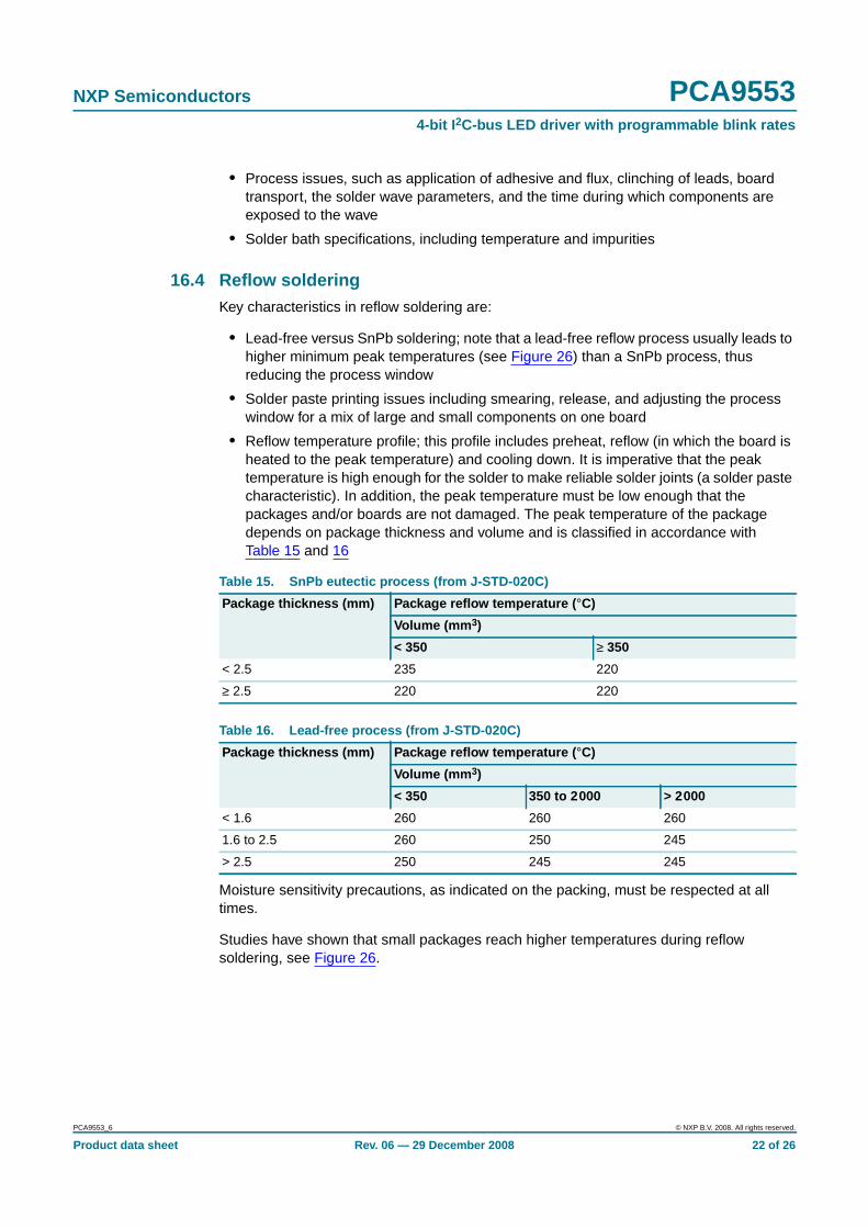
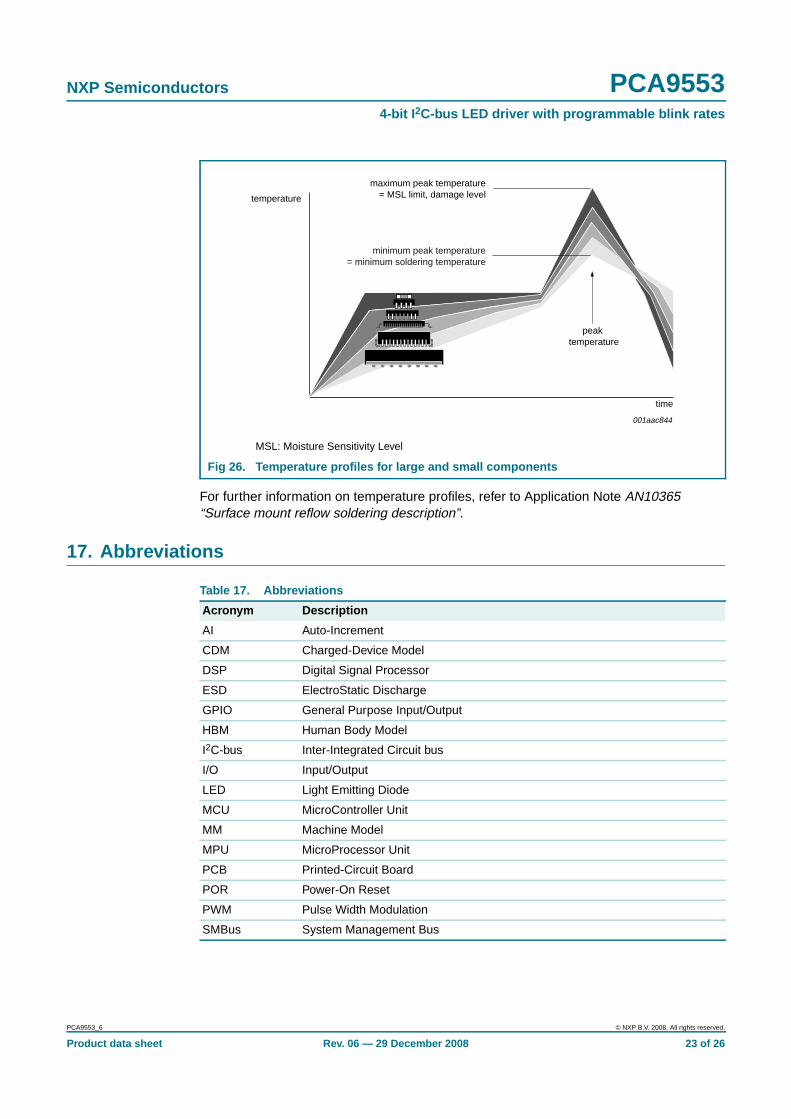
• Lead-free versus SnPb soldering; note that a lead-free reflow process usually leads tohigher minimum peak temperatures (see Figure 26) than a SnPb process, thusreducing the process window
• Solder paste printing issues including smearing, release, and adjusting the processwindow for a mix of large and small components on one board
• Reflow temperature profile; this profile includes preheat, reflow (in which the board isheated to the peak temperature) and cooling down. It is imperative that the peaktemperature is high enough for the solder to make reliable solder joints (a solder pastecharacteristic). In addition, the peak temperature must be low enough that thepackages and/or boards are not damaged. The peak temperature of the packagedepends on package thickness and volume and is classified in accordance withTable 15 and 16
Moisture sensitivity precautions, as indicated on the packing, must be respected at alltimes.
Studies have shown that small packages reach higher temperatures during reflowsoldering, see Figure 26.
Table 15. SnPb eutectic process (from J-STD-020C)
Package thickness (mm) Package reflow temperature ( °C)
Volume (mm 3)
< 350 ≥ 350
< 2.5 235 220
≥ 2.5 220 220
Table 16. Lead-free process (from J-STD-020C)
Package thickness (mm) Package reflow temperature ( °C)
Product data sheet Rev. 06 — 29 December 2008 24 of 26
NXP Semiconductors PCA95534-bit I 2C-bus LED driver with programmable blink rates
19. Legal information
19.1 Data sheet status
[1] Please consult the most recently issued document before initiating or completing a design.
[2] The term ‘short data sheet’ is explained in section “Definitions”.
[3] The product status of device(s) described in this document may have changed since this document was published and may differ in case of multiple devices. The latest product statusinformation is available on the Internet at URL http://www.nxp.com.
19.2 Definitions
Draft — The document is a draft version only. The content is still underinternal review and subject to formal approval, which may result inmodifications or additions. NXP Semiconductors does not give anyrepresentations or warranties as to the accuracy or completeness ofinformation included herein and shall have no liability for the consequences ofuse of such information.
Short data sheet — A short data sheet is an extract from a full data sheetwith the same product type number(s) and title. A short data sheet is intendedfor quick reference only and should not be relied upon to contain detailed andfull information. For detailed and full information see the relevant full datasheet, which is available on request via the local NXP Semiconductors salesoffice. In case of any inconsistency or conflict with the short data sheet, thefull data sheet shall prevail.
19.3 Disclaimers
General — Information in this document is believed to be accurate andreliable. However, NXP Semiconductors does not give any representations orwarranties, expressed or implied, as to the accuracy or completeness of suchinformation and shall have no liability for the consequences of use of suchinformation.
Right to make changes — NXP Semiconductors reserves the right to makechanges to information published in this document, including withoutlimitation specifications and product descriptions, at any time and withoutnotice. This document supersedes and replaces all information supplied priorto the publication hereof.
Suitability for use — NXP Semiconductors products are not designed,authorized or warranted to be suitable for use in medical, military, aircraft,space or life support equipment, nor in applications where failure ormalfunction of an NXP Semiconductors product can reasonably be expected
to result in personal injury, death or severe property or environmentaldamage. NXP Semiconductors accepts no liability for inclusion and/or use ofNXP Semiconductors products in such equipment or applications andtherefore such inclusion and/or use is at the customer’s own risk.
Applications — Applications that are described herein for any of theseproducts are for illustrative purposes only. NXP Semiconductors makes norepresentation or warranty that such applications will be suitable for thespecified use without further testing or modification.
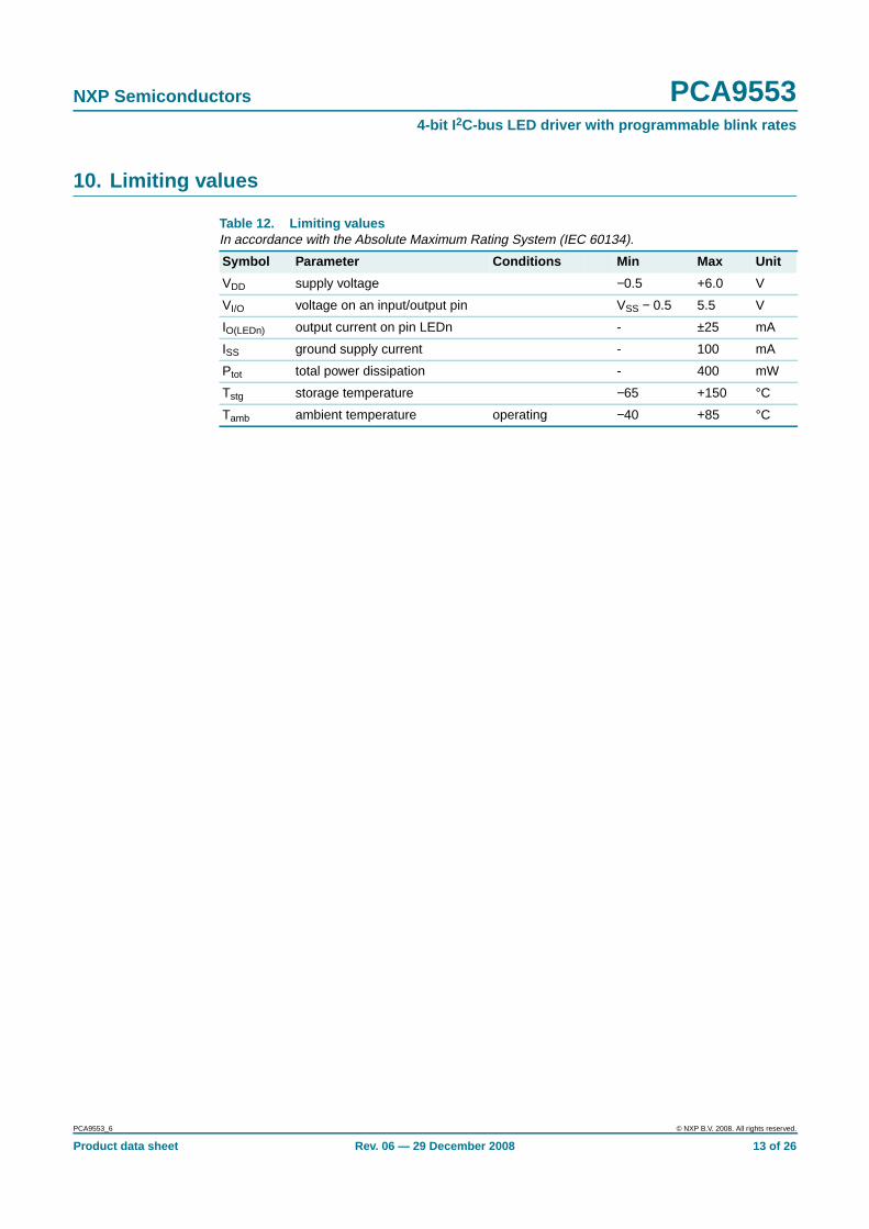
Limiting values — Stress above one or more limiting values (as defined inthe Absolute Maximum Ratings System of IEC 60134) may cause permanentdamage to the device. Limiting values are stress ratings only and operation ofthe device at these or any other conditions above those given in theCharacteristics sections of this document is not implied. Exposure to limitingvalues for extended periods may affect device reliability.
Terms and conditions of sale — NXP Semiconductors products are soldsubject to the general terms and conditions of commercial sale, as publishedat http://www.nxp.com/profile/terms, including those pertaining to warranty,intellectual property rights infringement and limitation of liability, unlessexplicitly otherwise agreed to in writing by NXP Semiconductors. In case ofany inconsistency or conflict between information in this document and suchterms and conditions, the latter will prevail.
No offer to sell or license — Nothing in this document may be interpretedor construed as an offer to sell products that is open for acceptance or thegrant, conveyance or implication of any license under any copyrights, patentsor other industrial or intellectual property rights.
19.4 TrademarksNotice: All referenced brands, product names, service names and trademarksare the property of their respective owners.
I2C-bus — logo is a trademark of NXP B.V.
20. Contact information
For more information, please visit: http://www .nxp.com
For sales office addresses, please send an email to: salesad [email protected]
Document status [1] [2] Product status [3] Definition
Objective [short] data sheet Development This document contains data from the objective specification for product development.
Preliminary [short] data sheet Qualification This document contains data from the preliminary specification.
Product [short] data sheet Production This document contains the product specification.