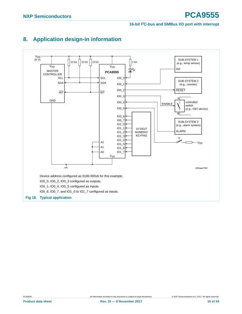
1. General description The PCA9555 is a 24-pin CMOS device that provides 16 bits of General Purpose parallel Input/Output (GPIO) expansion for I 2 C-bus/SMBus applications and was developed to enhance the NXP Semiconductors family of I 2 C-bus I/O expanders. The improvements include higher drive capability, 5 V I/O tolerance, lower supply current, individual I/O configuration, and smaller packaging. I/O expanders provide a simple solution when additional I/O is needed for ACPI power switches, sensors, push buttons, LEDs, fans, etc. The PCA9555 consists of two 8-bit Configuration (Input or Output selection); Input, Output and Polarity Inversion (active HIGH or active LOW operation) registers. The system master can enable the I/Os as either inputs or outputs by writing to the I/O configuration bits. The data for each Input or Output is kept in the corresponding Input or Output register. The polarity of the read register can be inverted with the Polarity Inversion register. All registers can be read by the system master. Although pin-to-pin and I 2 C-bus address compatible with the PCF8575, software changes are required due to the enhancements, and are discussed in Application Note AN469. The PCA9555 open-drain interrupt output is activated when any input state differs from its corresponding input port register state and is used to indicate to the system master that an input state has changed. The power-on reset sets the registers to their default values and initializes the device state machine. Three hardware pins (A0, A1, A2) vary the fixed I 2 C-bus address and allow up to eight devices to share the same I 2 C-bus/SMBus. The fixed I 2 C-bus address of the PCA9555 is the same as the PCA9554, allowing up to eight of these devices in any combination to share the same I 2 C-bus/SMBus. 2. Features and benefits Operating power supply voltage range of 2.3 V to 5.5 V 5 V tolerant I/Os Polarity Inversion register Active LOW interrupt output Low standby current Noise filter on SCL/SDA inputs No glitch on power-up Internal power-on reset 16 I/O pins which default to 16 inputs 0 Hz to 400 kHz clock frequency ESD protection exceeds 2000 V HBM per JESD22-A114, 200 V MM per JESD22-A115, and 1000 V CDM per JESD22-C101 PCA9555 16-bit I 2 C-bus and SMBus I/O port with interrupt Rev. 10 — 8 November 2017 Product data sheet
Transcript
1. General description
The PCA9555 is a 24-pin CMOS device that provides 16 bits of General Purpose parallel Input/Output (GPIO) expansion for I2C-bus/SMBus applications and was developed to enhance the NXP Semiconductors family of I2C-bus I/O expanders. The improvements include higher drive capability, 5 V I/O tolerance, lower supply current, individual I/O configuration, and smaller packaging. I/O expanders provide a simple solution when additional I/O is needed for ACPI power switches, sensors, push buttons, LEDs, fans, etc.
The PCA9555 consists of two 8-bit Configuration (Input or Output selection); Input, Output and Polarity Inversion (active HIGH or active LOW operation) registers. The system master can enable the I/Os as either inputs or outputs by writing to the I/O configuration bits. The data for each Input or Output is kept in the corresponding Input or Output register. The polarity of the read register can be inverted with the Polarity Inversion register. All registers can be read by the system master. Although pin-to-pin and I2C-bus address compatible with the PCF8575, software changes are required due to the enhancements, and are discussed in Application Note AN469.
The PCA9555 open-drain interrupt output is activated when any input state differs from its corresponding input port register state and is used to indicate to the system master that an input state has changed. The power-on reset sets the registers to their default values and initializes the device state machine.
Three hardware pins (A0, A1, A2) vary the fixed I2C-bus address and allow up to eight devices to share the same I2C-bus/SMBus. The fixed I2C-bus address of the PCA9555 is the same as the PCA9554, allowing up to eight of these devices in any combination to share the same I2C-bus/SMBus.
2. Features and benefits
Operating power supply voltage range of 2.3 V to 5.5 V
5 V tolerant I/Os
Polarity Inversion register
Active LOW interrupt output
Low standby current
Noise filter on SCL/SDA inputs
No glitch on power-up
Internal power-on reset
16 I/O pins which default to 16 inputs
0 Hz to 400 kHz clock frequency
ESD protection exceeds 2000 V HBM per JESD22-A114, 200 V MM per JESD22-A115, and 1000 V CDM per JESD22-C101
PCA955516-bit I2C-bus and SMBus I/O port with interruptRev. 10 — 8 November 2017 Product data sheet
NXP Semiconductors PCA955516-bit I2C-bus and SMBus I/O port with interrupt
Latch-up testing is done to JEDEC Standard JESD78 which exceeds 100 mA
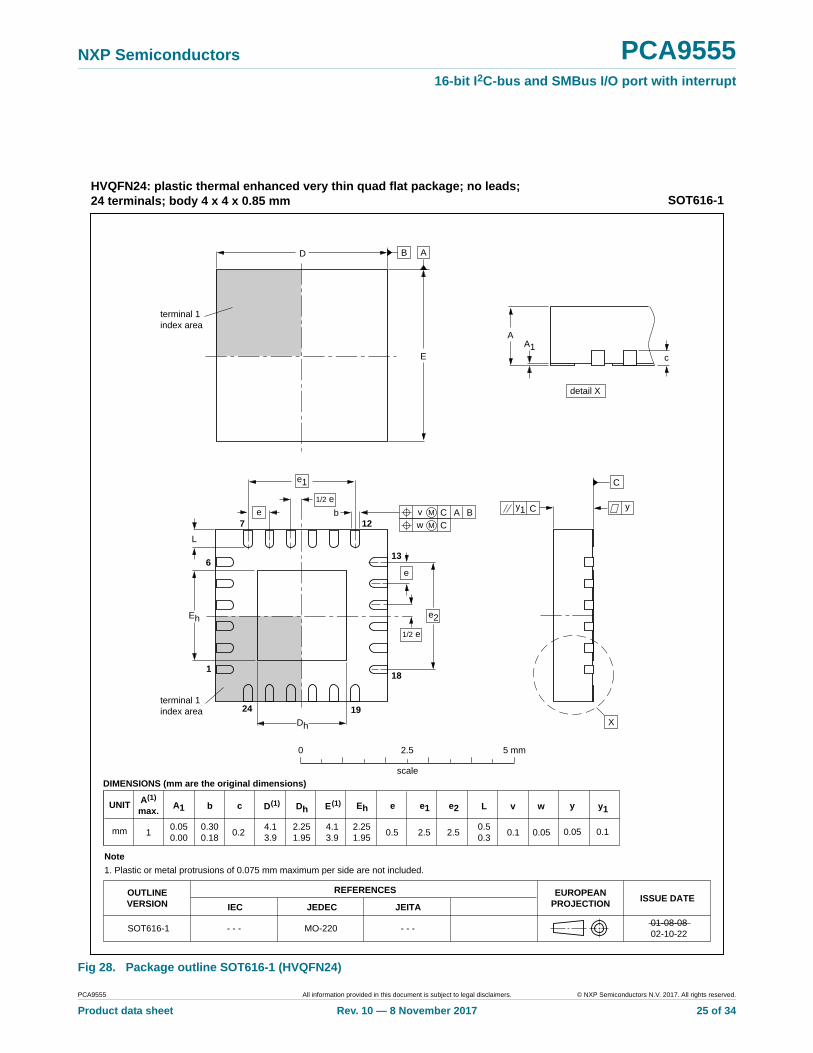
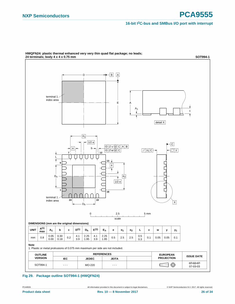
Five packages offered: SO24, SSOP24, TSSOP24, HVQFN24 and HWQFN24
3. Ordering information
3.1 Ordering options
Table 1. Ordering information
Type number Topside mark Package
Name Description Version
PCA9555D PCA9555D SO24 plastic small outline package; 24 leads; body width 7.5 mm
SOT137-1
PCA9555DB PCA9555 SSOP24 plastic shrink small outline package; 24 leads; bodywidth 5.3 mm
SOT340-1
PCA9555PW PCA9555 TSSOP24 plastic thin shrink small outline package; 24 leads; body width 4.4 mm
SOT355-1
PCA9555BS 9555 HVQFN24 plastic thermal enhanced very thin quad flat package; no leads; 24 terminals; body 4 4 0.85 mm
SOT616-1
PCA9555HF P55H HWQFN24 plastic thermal enhanced very very thin quad flat package; no leads; 24 terminals; body 4 4 0.75 mm
Product data sheet Rev. 10 — 8 November 2017 4 of 34
NXP Semiconductors PCA955516-bit I2C-bus and SMBus I/O port with interrupt
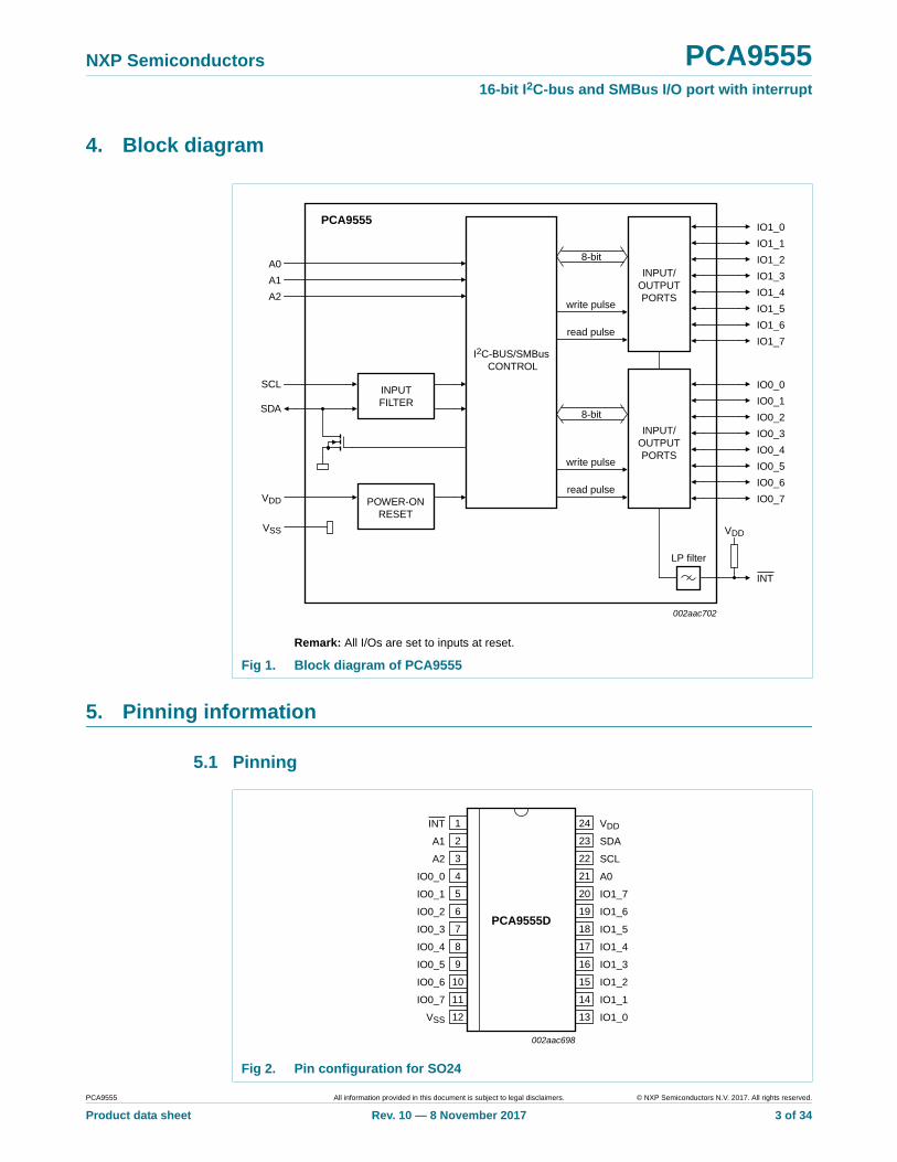
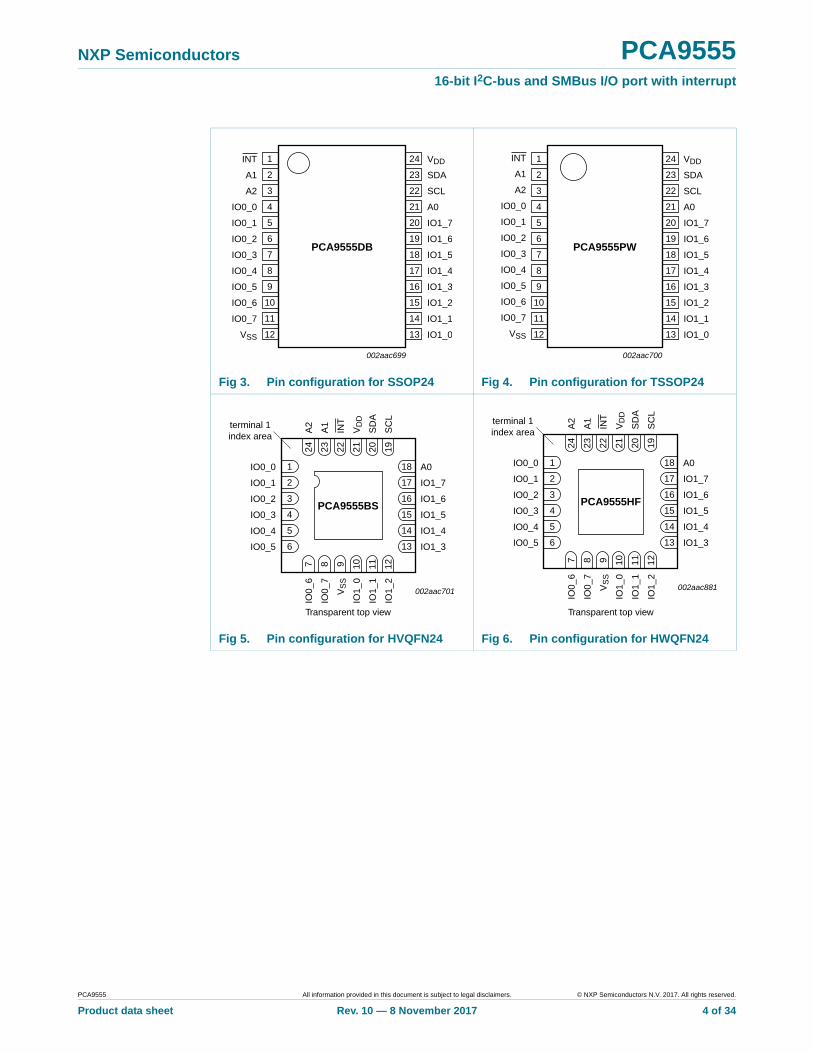
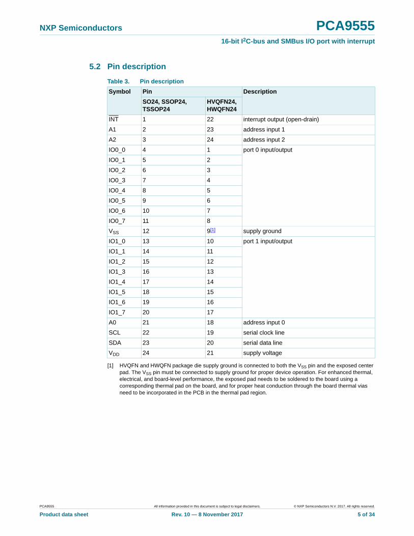
5.2 Pin description
[1] HVQFN and HWQFN package die supply ground is connected to both the VSS pin and the exposed center pad. The VSS pin must be connected to supply ground for proper device operation. For enhanced thermal, electrical, and board-level performance, the exposed pad needs to be soldered to the board using a corresponding thermal pad on the board, and for proper heat conduction through the board thermal vias need to be incorporated in the PCB in the thermal pad region.
Product data sheet Rev. 10 — 8 November 2017 5 of 34
NXP Semiconductors PCA955516-bit I2C-bus and SMBus I/O port with interrupt
6. Functional description
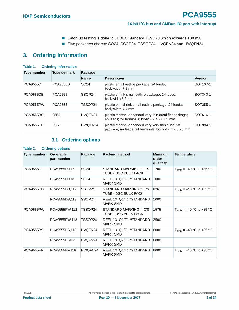
Refer to Figure 1 “Block diagram of PCA9555”.
6.1 Device address
6.2 Registers
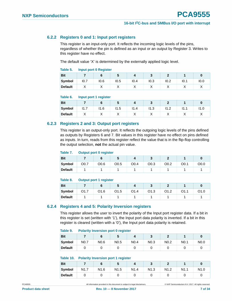
6.2.1 Command byte
The command byte is the first byte to follow the address byte during a write transmission. It is used as a pointer to determine which of the following registers will be written or read.
Product data sheet Rev. 10 — 8 November 2017 6 of 34
NXP Semiconductors PCA955516-bit I2C-bus and SMBus I/O port with interrupt
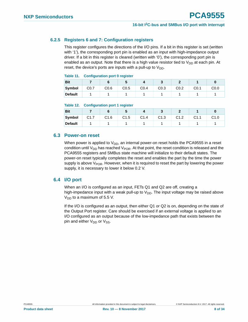
6.2.2 Registers 0 and 1: Input port registers
This register is an input-only port. It reflects the incoming logic levels of the pins, regardless of whether the pin is defined as an input or an output by Register 3. Writes to this register have no effect.
The default value ‘X’ is determined by the externally applied logic level.
6.2.3 Registers 2 and 3: Output port registers
This register is an output-only port. It reflects the outgoing logic levels of the pins defined as outputs by Registers 6 and 7. Bit values in this register have no effect on pins defined as inputs. In turn, reads from this register reflect the value that is in the flip-flop controlling the output selection, not the actual pin value.
6.2.4 Registers 4 and 5: Polarity Inversion registers
This register allows the user to invert the polarity of the Input port register data. If a bit in this register is set (written with ‘1’), the Input port data polarity is inverted. If a bit in this register is cleared (written with a ‘0’), the Input port data polarity is retained.
Product data sheet Rev. 10 — 8 November 2017 7 of 34
NXP Semiconductors PCA955516-bit I2C-bus and SMBus I/O port with interrupt
6.2.5 Registers 6 and 7: Configuration registers
This register configures the directions of the I/O pins. If a bit in this register is set (written with ‘1’), the corresponding port pin is enabled as an input with high-impedance output driver. If a bit in this register is cleared (written with ‘0’), the corresponding port pin is enabled as an output. Note that there is a high value resistor tied to VDD at each pin. At reset, the device's ports are inputs with a pull-up to VDD.
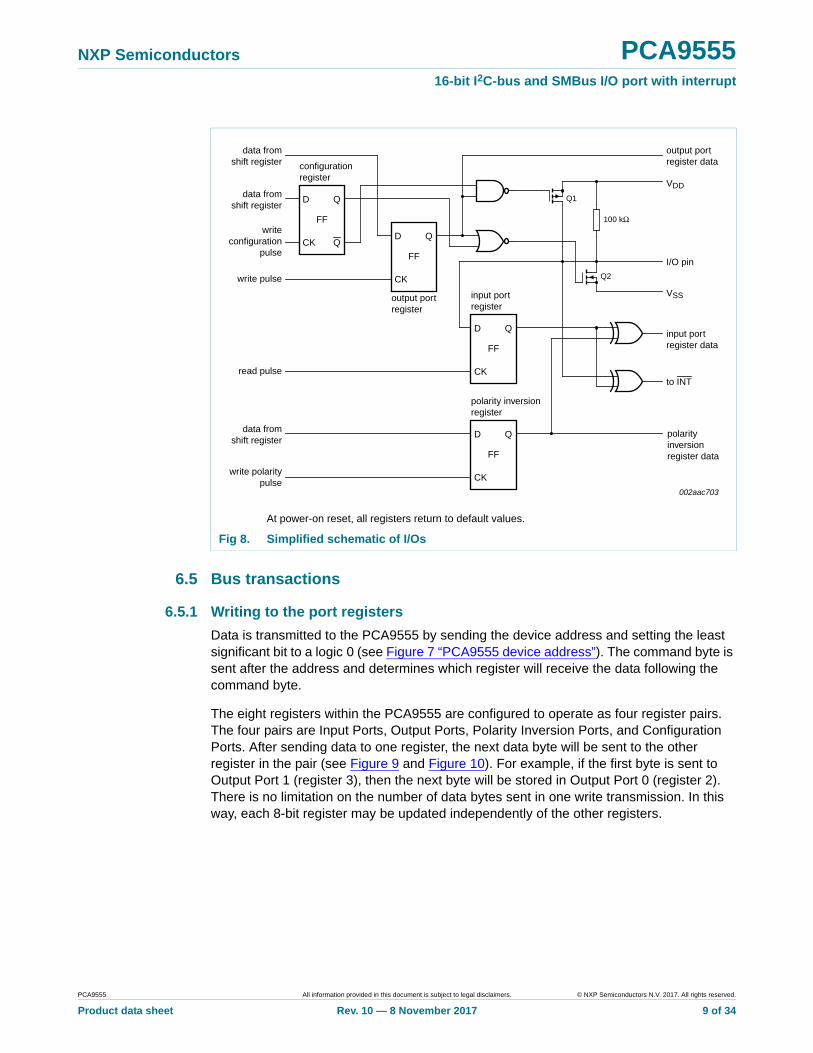
6.3 Power-on reset
When power is applied to VDD, an internal power-on reset holds the PCA9555 in a reset condition until VDD has reached VPOR. At that point, the reset condition is released and the PCA9555 registers and SMBus state machine will initialize to their default states. The power-on reset typically completes the reset and enables the part by the time the power supply is above VPOR. However, when it is required to reset the part by lowering the power supply, it is necessary to lower it below 0.2 V.
6.4 I/O port
When an I/O is configured as an input, FETs Q1 and Q2 are off, creating a high-impedance input with a weak pull-up to VDD. The input voltage may be raised above VDD to a maximum of 5.5 V.
If the I/O is configured as an output, then either Q1 or Q2 is on, depending on the state of the Output Port register. Care should be exercised if an external voltage is applied to an I/O configured as an output because of the low-impedance path that exists between the pin and either VDD or VSS.
Product data sheet Rev. 10 — 8 November 2017 8 of 34
NXP Semiconductors PCA955516-bit I2C-bus and SMBus I/O port with interrupt
6.5 Bus transactions
6.5.1 Writing to the port registers
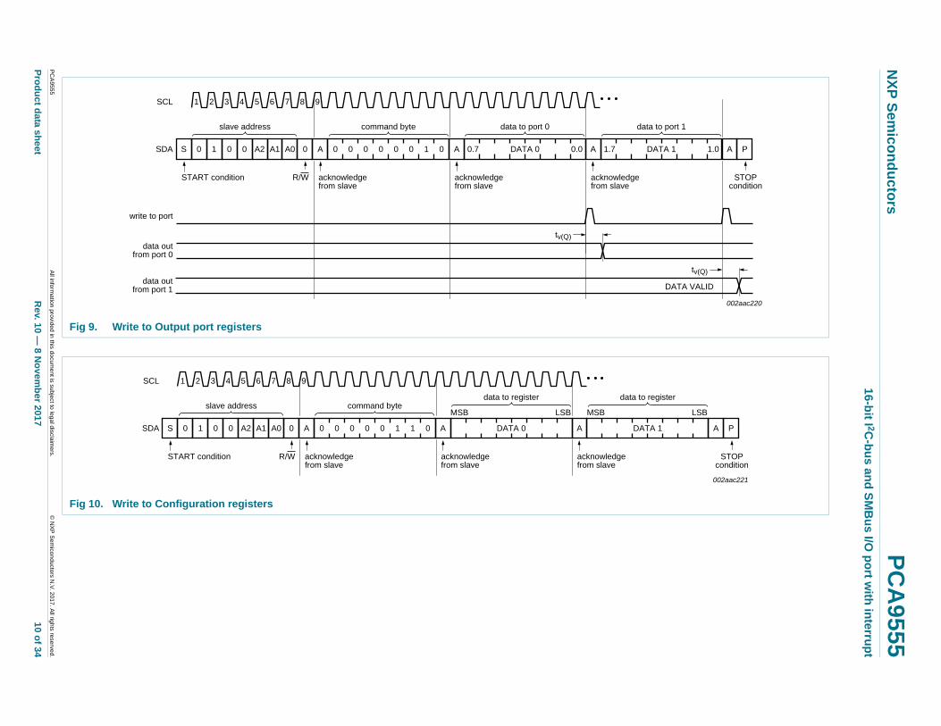
Data is transmitted to the PCA9555 by sending the device address and setting the least significant bit to a logic 0 (see Figure 7 “PCA9555 device address”). The command byte is sent after the address and determines which register will receive the data following the command byte.
The eight registers within the PCA9555 are configured to operate as four register pairs. The four pairs are Input Ports, Output Ports, Polarity Inversion Ports, and Configuration Ports. After sending data to one register, the next data byte will be sent to the other register in the pair (see Figure 9 and Figure 10). For example, if the first byte is sent to Output Port 1 (register 3), then the next byte will be stored in Output Port 0 (register 2). There is no limitation on the number of data bytes sent in one write transmission. In this way, each 8-bit register may be updated independently of the other registers.
At power-on reset, all registers return to default values.
Product data sheet Rev. 10 — 8 November 2017 9 of 34
xxxxxxxxxxxxxxxxxxxxx xxxxxxxxxxxxxxxxxxxxxxxxxx xxxxxxx x x x xxxxxxxxxxxxxxxxxxxxxxxxxxxxxx xxxxxxxxxxxxxxxxxxx xx xx xxxxx xxxxxxxxxxxxxxxxxxxxxxxxxxx xxxxxxxxxxxxxxxxxxx xxxxxx xxxxxxxxxxxxxxxxxxxxxxxxxxxxxxxxxxx xxxxxxxxxxxx x x xxxxxxxxxxxxxxxxxxxxx xxxxxxxxxxxxxxxxxxxxxxxxxxxxxx xxxxx xxxxxxxxxxxxxxxxxxxxxxxxxxxxxxxxxxxxxxxxxxxxxxxxxx xxxxxxxx xxxxxxxxxxxxxxxxxxxxxxxxx xxxxxxxxxxxxxxxxxxxx xxx
NXP Semiconductors PCA955516-bit I2C-bus and SMBus I/O port with interrupt
6.5.2 Reading the port registers
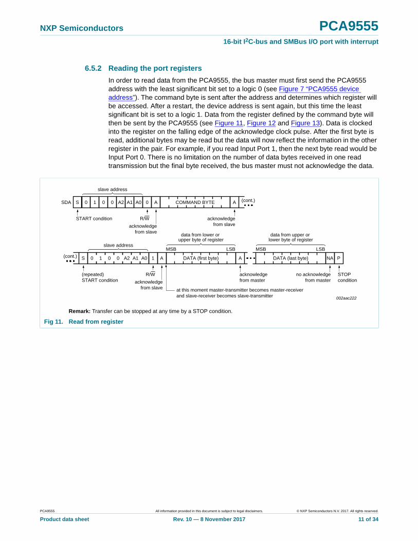
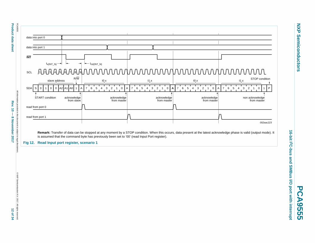
In order to read data from the PCA9555, the bus master must first send the PCA9555 address with the least significant bit set to a logic 0 (see Figure 7 “PCA9555 device address”). The command byte is sent after the address and determines which register will be accessed. After a restart, the device address is sent again, but this time the least significant bit is set to a logic 1. Data from the register defined by the command byte will then be sent by the PCA9555 (see Figure 11, Figure 12 and Figure 13). Data is clocked into the register on the falling edge of the acknowledge clock pulse. After the first byte is read, additional bytes may be read but the data will now reflect the information in the other register in the pair. For example, if you read Input Port 1, then the next byte read would be Input Port 0. There is no limitation on the number of data bytes received in one read transmission but the final byte received, the bus master must not acknowledge the data.
Remark: Transfer can be stopped at any time by a STOP condition.
Fig 11. Read from register
AS
START condition R/W
acknowledgefrom slave
002aac222
A
acknowledgefrom slave
SDA
A P
acknowledgefrom master
DATA (first byte)
slave address
STOPcondition
S
(repeated)START condition
(cont.)
(cont.) 1 0 0 A2 A1 A0 1 A0
R/W
acknowledgefrom slave
slave address
at this moment master-transmitter becomes master-receiverand slave-receiver becomes slave-transmitter
Product data sheet Rev. 10 — 8 November 2017 11 of 34
xxxxxxxxxxxxxxxxxxxxx xxxxxxxxxxxxxxxxxxxxxxxxxx xxxxxxx x x x xxxxxxxxxxxxxxxxxxxxxxxxxxxxxx xxxxxxxxxxxxxxxxxxx xx xx xxxxx xxxxxxxxxxxxxxxxxxxxxxxxxxx xxxxxxxxxxxxxxxxxxx xxxxxx xxxxxxxxxxxxxxxxxxxxxxxxxxxxxxxxxxx xxxxxxxxxxxx x x xxxxxxxxxxxxxxxxxxxxx xxxxxxxxxxxxxxxxxxxxxxxxxxxxxx xxxxx xxxxxxxxxxxxxxxxxxxxxxxxxxxxxxxxxxxxxxxxxxxxxxxxxx xxxxxxxx xxxxxxxxxxxxxxxxxxxxxxxxx xxxxxxxxxxxxxxxxxxxx xxx
Remark: Transfer of data can be stopped at any moment by a STOP condition. When this occurs, data present at the latest acknowleis assumed that the command byte has previously been set to ‘00’ (read Input Port register).
Fig 12. Read Input port register, scenario 1
1 0 0 A2 A1 A0 1 AS 0
START condition
R/W
acknowledgefrom slave
A
SCL
SDA A
read from port 0
987654321
I0.xslave address
acknowledgefrom master
A
I1.x
acknowledgefrom master
A
I0.x
acknowledgefrom master
data into port 0
read from port 1
data into port 1
INT
6 5 4 3 2 1 07 6 5 4 3 2 1 07 6 5 4 3 2 1 07 7
INT
tv(INT_N) trst(INT_N)
xxxxxxxxxxxxxxxxxxxxx xxxxxxxxxxxxxxxxxxxxxxxxxx xxxxxxx x x x xxxxxxxxxxxxxxxxxxxxxxxxxxxxxx xxxxxxxxxxxxxxxxxxx xx xx xxxxx xxxxxxxxxxxxxxxxxxxxxxxxxxx xxxxxxxxxxxxxxxxxxx xxxxxx xxxxxxxxxxxxxxxxxxxxxxxxxxxxxxxxxxx xxxxxxxxxxxx x x xxxxxxxxxxxxxxxxxxxxx xxxxxxxxxxxxxxxxxxxxxxxxxxxxxx xxxxx xxxxxxxxxxxxxxxxxxxxxxxxxxxxxxxxxxxxxxxxxxxxxxxxxx xxxxxxxx xxxxxxxxxxxxxxxxxxxxxxxxx xxxxxxxxxxxxxxxxxxxx xxx
Remark: Transfer of data can be stopped at any moment by a STOP condition. When this occurs, data present at the latest acknowleis assumed that the command byte has previously been set to ‘00’ (read Input Port register).
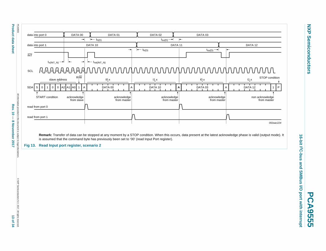
Fig 13. Read Input port register, scenario 2
1 0 0 A2 A1 A0 1 AS 0
START condition
R/W
acknowledgefrom slave
A
SCL
SDA A
read from port 0
987654321
I0.xslave address
acknowledgefrom master
A
I1.x
acknowledgefrom master
A
I0.x
acknowledgefrom master
data into port 0
read from port 1
data into port 1
INT
tv(INT_N) trst(INT_N)
DATA 00 DATA 10 DATA 03
DATA 00 DATA 01
th(D)
th(D)
DATA 02
tsu(D)
DATA 03
tsu(D)
DATA 10 DATA 11
NXP Semiconductors PCA955516-bit I2C-bus and SMBus I/O port with interrupt
6.5.3 Interrupt output
The open-drain interrupt output is activated when one of the port pins changes state and the pin is configured as an input. The interrupt is deactivated when the input returns to its previous state or the Input Port register is read (see Figure 12). A pin configured as an output cannot cause an interrupt. Since each 8-bit port is read independently, the interrupt caused by Port 0 will not be cleared by a read of Port 1 or the other way around.
Remark: Changing an I/O from an output to an input may cause a false interrupt to occur if the state of the pin does not match the contents of the Input Port register.
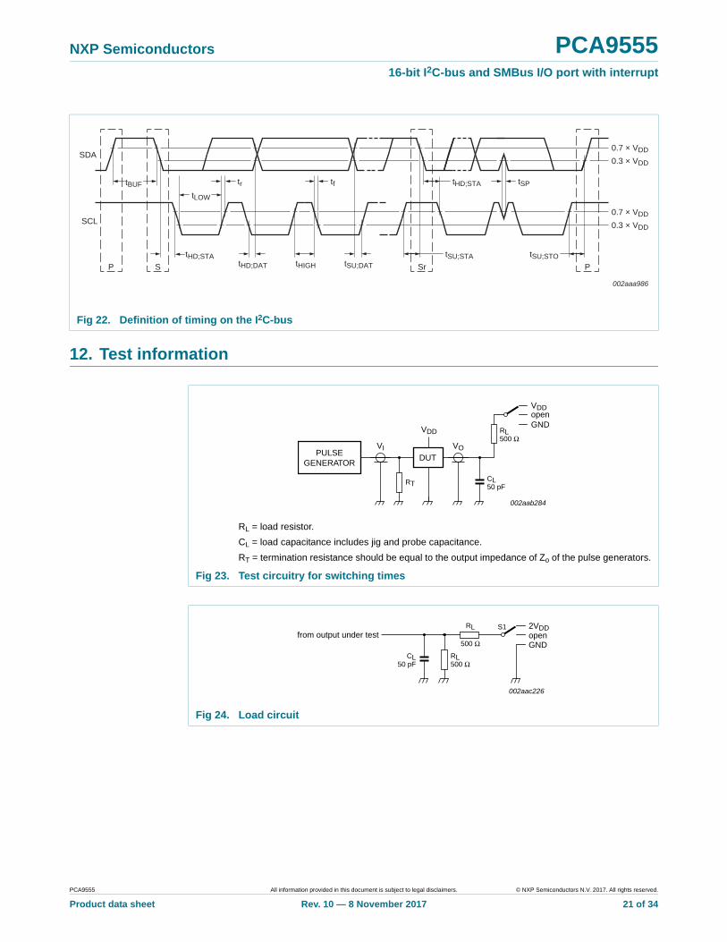
7. Characteristics of the I2C-bus
The I2C-bus is for 2-way, 2-line communication between different ICs or modules. The two lines are a serial data line (SDA) and a serial clock line (SCL). Both lines must be connected to a positive supply via a pull-up resistor when connected to the output stages of a device. Data transfer may be initiated only when the bus is not busy.
7.1 Bit transfer
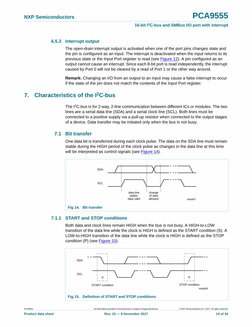
One data bit is transferred during each clock pulse. The data on the SDA line must remain stable during the HIGH period of the clock pulse as changes in the data line at this time will be interpreted as control signals (see Figure 14).
7.1.1 START and STOP conditions
Both data and clock lines remain HIGH when the bus is not busy. A HIGH-to-LOW transition of the data line while the clock is HIGH is defined as the START condition (S). A LOW-to-HIGH transition of the data line while the clock is HIGH is defined as the STOP condition (P) (see Figure 15).
Product data sheet Rev. 10 — 8 November 2017 14 of 34
NXP Semiconductors PCA955516-bit I2C-bus and SMBus I/O port with interrupt
7.2 System configuration
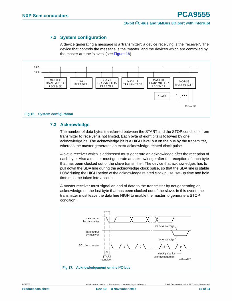
A device generating a message is a ‘transmitter’; a device receiving is the ‘receiver’. The device that controls the message is the ‘master’ and the devices which are controlled by the master are the ‘slaves’ (see Figure 16).
7.3 Acknowledge
The number of data bytes transferred between the START and the STOP conditions from transmitter to receiver is not limited. Each byte of eight bits is followed by one acknowledge bit. The acknowledge bit is a HIGH level put on the bus by the transmitter, whereas the master generates an extra acknowledge related clock pulse.
A slave receiver which is addressed must generate an acknowledge after the reception of each byte. Also a master must generate an acknowledge after the reception of each byte that has been clocked out of the slave transmitter. The device that acknowledges has to pull down the SDA line during the acknowledge clock pulse, so that the SDA line is stable LOW during the HIGH period of the acknowledge related clock pulse; set-up time and hold time must be taken into account.
A master receiver must signal an end of data to the transmitter by not generating an acknowledge on the last byte that has been clocked out of the slave. In this event, the transmitter must leave the data line HIGH to enable the master to generate a STOP condition.
Product data sheet Rev. 10 — 8 November 2017 18 of 34
NXP Semiconductors PCA955516-bit I2C-bus and SMBus I/O port with interrupt
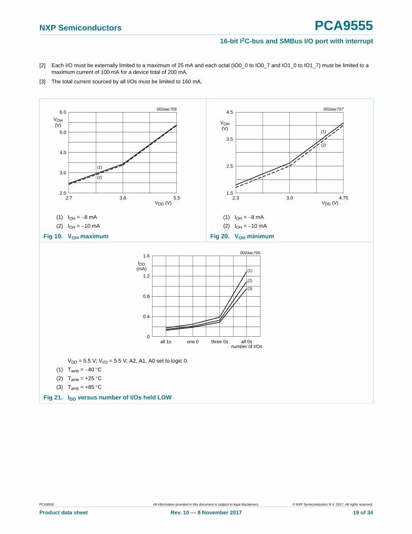
[2] Each I/O must be externally limited to a maximum of 25 mA and each octal (IO0_0 to IO0_7 and IO1_0 to IO1_7) must be limited to a maximum current of 100 mA for a device total of 200 mA.
[3] The total current sourced by all I/Os must be limited to 160 mA.
(1) IOH = 8 mA
(2) IOH = 10 mA
(1) IOH = 8 mA
(2) IOH = 10 mA
Fig 19. VOH maximum Fig 20. VOH minimum
VDD = 5.5 V; VI/O = 5.5 V; A2, A1, A0 set to logic 0.
Product data sheet Rev. 10 — 8 November 2017 26 of 34
NXP Semiconductors PCA955516-bit I2C-bus and SMBus I/O port with interrupt
14. Handling information
All input and output pins are protected against ElectroStatic Discharge (ESD) under normal handling. When handling ensure that the appropriate precautions are taken as described in JESD625-A or equivalent standards.
15. Soldering of SMD packages
This text provides a very brief insight into a complex technology. A more in-depth account of soldering ICs can be found in Application Note AN10365 “Surface mount reflow soldering description”.
15.1 Introduction to soldering
Soldering is one of the most common methods through which packages are attached to Printed Circuit Boards (PCBs), to form electrical circuits. The soldered joint provides both the mechanical and the electrical connection. There is no single soldering method that is ideal for all IC packages. Wave soldering is often preferred when through-hole and Surface Mount Devices (SMDs) are mixed on one printed wiring board; however, it is not suitable for fine pitch SMDs. Reflow soldering is ideal for the small pitches and high densities that come with increased miniaturization.
15.2 Wave and reflow soldering
Wave soldering is a joining technology in which the joints are made by solder coming from a standing wave of liquid solder. The wave soldering process is suitable for the following:
• Through-hole components
• Leaded or leadless SMDs, which are glued to the surface of the printed circuit board
Not all SMDs can be wave soldered. Packages with solder balls, and some leadless packages which have solder lands underneath the body, cannot be wave soldered. Also, leaded SMDs with leads having a pitch smaller than ~0.6 mm cannot be wave soldered, due to an increased probability of bridging.
The reflow soldering process involves applying solder paste to a board, followed by component placement and exposure to a temperature profile. Leaded packages, packages with solder balls, and leadless packages are all reflow solderable.
Key characteristics in both wave and reflow soldering are:
• Board specifications, including the board finish, solder masks and vias
• Package footprints, including solder thieves and orientation
Product data sheet Rev. 10 — 8 November 2017 27 of 34
NXP Semiconductors PCA955516-bit I2C-bus and SMBus I/O port with interrupt
• Process issues, such as application of adhesive and flux, clinching of leads, board transport, the solder wave parameters, and the time during which components are exposed to the wave
• Solder bath specifications, including temperature and impurities
15.4 Reflow soldering
Key characteristics in reflow soldering are:
• Lead-free versus SnPb soldering; note that a lead-free reflow process usually leads to higher minimum peak temperatures (see Figure 30) than a SnPb process, thus reducing the process window
• Solder paste printing issues including smearing, release, and adjusting the process window for a mix of large and small components on one board
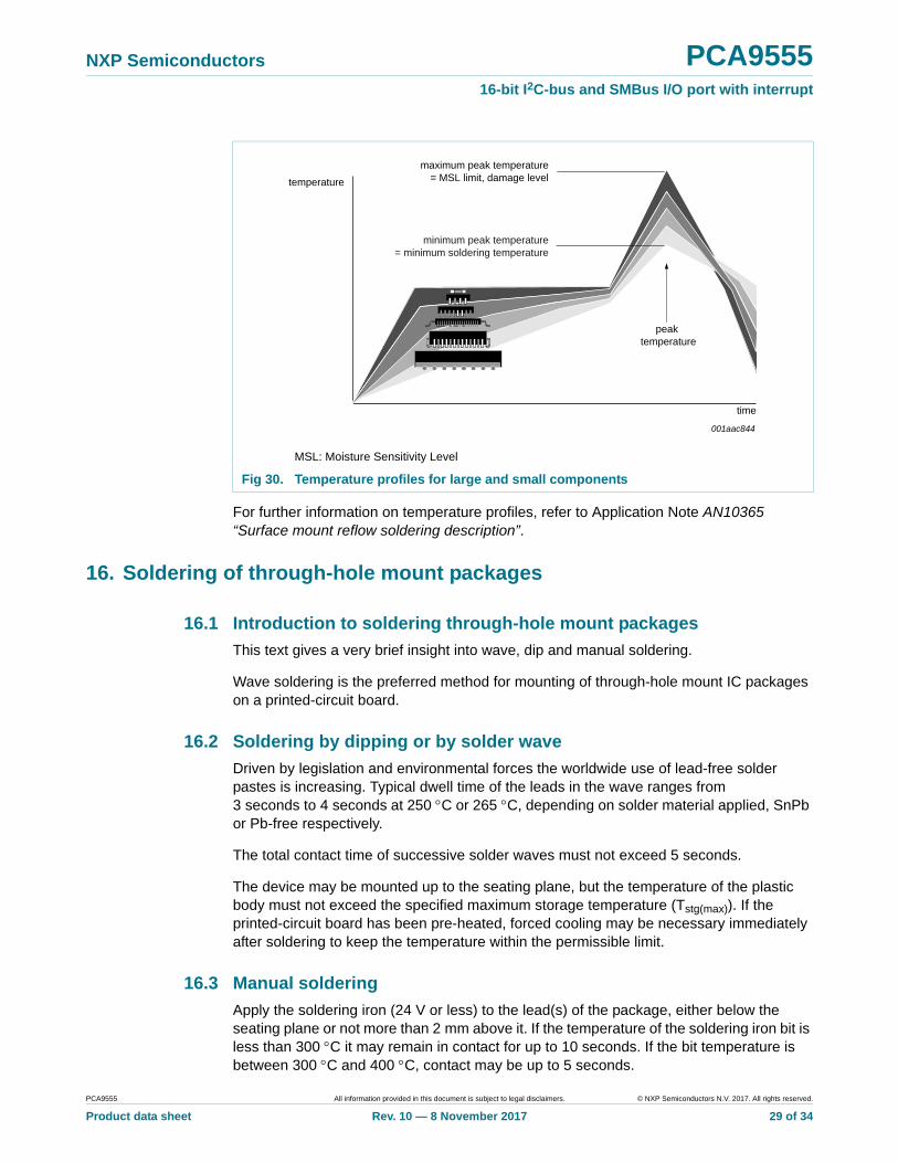
• Reflow temperature profile; this profile includes preheat, reflow (in which the board is heated to the peak temperature) and cooling down. It is imperative that the peak temperature is high enough for the solder to make reliable solder joints (a solder paste characteristic). In addition, the peak temperature must be low enough that the packages and/or boards are not damaged. The peak temperature of the package depends on package thickness and volume and is classified in accordance with Table 16 and 17
Moisture sensitivity precautions, as indicated on the packing, must be respected at all times.
Studies have shown that small packages reach higher temperatures during reflow soldering, see Figure 30.
Table 16. SnPb eutectic process (from J-STD-020C)
Package thickness (mm) Package reflow temperature (C)
Volume (mm3)
< 350 350
< 2.5 235 220
2.5 220 220
Table 17. Lead-free process (from J-STD-020C)
Package thickness (mm) Package reflow temperature (C)
Product data sheet Rev. 10 — 8 November 2017 28 of 34
NXP Semiconductors PCA955516-bit I2C-bus and SMBus I/O port with interrupt
For further information on temperature profiles, refer to Application Note AN10365 “Surface mount reflow soldering description”.
16. Soldering of through-hole mount packages
16.1 Introduction to soldering through-hole mount packages
This text gives a very brief insight into wave, dip and manual soldering.
Wave soldering is the preferred method for mounting of through-hole mount IC packages on a printed-circuit board.
16.2 Soldering by dipping or by solder wave
Driven by legislation and environmental forces the worldwide use of lead-free solder pastes is increasing. Typical dwell time of the leads in the wave ranges from 3 seconds to 4 seconds at 250 C or 265 C, depending on solder material applied, SnPb or Pb-free respectively.
The total contact time of successive solder waves must not exceed 5 seconds.
The device may be mounted up to the seating plane, but the temperature of the plastic body must not exceed the specified maximum storage temperature (Tstg(max)). If the printed-circuit board has been pre-heated, forced cooling may be necessary immediately after soldering to keep the temperature within the permissible limit.
16.3 Manual soldering
Apply the soldering iron (24 V or less) to the lead(s) of the package, either below the seating plane or not more than 2 mm above it. If the temperature of the soldering iron bit is less than 300 C it may remain in contact for up to 10 seconds. If the bit temperature is between 300 C and 400 C, contact may be up to 5 seconds.
MSL: Moisture Sensitivity Level
Fig 30. Temperature profiles for large and small components
001aac844
temperature
time
minimum peak temperature= minimum soldering temperature
Product data sheet Rev. 10 — 8 November 2017 31 of 34
NXP Semiconductors PCA955516-bit I2C-bus and SMBus I/O port with interrupt
19. Legal information
19.1 Data sheet status
[1] Please consult the most recently issued document before initiating or completing a design.
[2] The term ‘short data sheet’ is explained in section “Definitions”.
[3] The product status of device(s) described in this document may have changed since this document was published and may differ in case of multiple devices. The latest product status information is available on the Internet at URL http://www.nxp.com.
19.2 Definitions
Draft — The document is a draft version only. The content is still under internal review and subject to formal approval, which may result in modifications or additions. NXP Semiconductors does not give any representations or warranties as to the accuracy or completeness of information included herein and shall have no liability for the consequences of use of such information.
Short data sheet — A short data sheet is an extract from a full data sheet with the same product type number(s) and title. A short data sheet is intended for quick reference only and should not be relied upon to contain detailed and full information. For detailed and full information see the relevant full data sheet, which is available on request via the local NXP Semiconductors sales office. In case of any inconsistency or conflict with the short data sheet, the full data sheet shall prevail.
Product specification — The information and data provided in a Product data sheet shall define the specification of the product as agreed between NXP Semiconductors and its customer, unless NXP Semiconductors and customer have explicitly agreed otherwise in writing. In no event however, shall an agreement be valid in which the NXP Semiconductors product is deemed to offer functions and qualities beyond those described in the Product data sheet.
19.3 Disclaimers
Limited warranty and liability — Information in this document is believed to be accurate and reliable. However, NXP Semiconductors does not give any representations or warranties, expressed or implied, as to the accuracy or completeness of such information and shall have no liability for the consequences of use of such information. NXP Semiconductors takes no responsibility for the content in this document if provided by an information source outside of NXP Semiconductors.
In no event shall NXP Semiconductors be liable for any indirect, incidental, punitive, special or consequential damages (including - without limitation - lost profits, lost savings, business interruption, costs related to the removal or replacement of any products or rework charges) whether or not such damages are based on tort (including negligence), warranty, breach of contract or any other legal theory.
Notwithstanding any damages that customer might incur for any reason whatsoever, NXP Semiconductors’ aggregate and cumulative liability towards customer for the products described herein shall be limited in accordance with the Terms and conditions of commercial sale of NXP Semiconductors.
Right to make changes — NXP Semiconductors reserves the right to make changes to information published in this document, including without limitation specifications and product descriptions, at any time and without notice. This document supersedes and replaces all information supplied prior to the publication hereof.
Suitability for use — NXP Semiconductors products are not designed, authorized or warranted to be suitable for use in life support, life-critical or safety-critical systems or equipment, nor in applications where failure or malfunction of an NXP Semiconductors product can reasonably be expected to result in personal injury, death or severe property or environmental damage. NXP Semiconductors and its suppliers accept no liability for inclusion and/or use of NXP Semiconductors products in such equipment or applications and therefore such inclusion and/or use is at the customer’s own risk.
Applications — Applications that are described herein for any of these products are for illustrative purposes only. NXP Semiconductors makes no representation or warranty that such applications will be suitable for the specified use without further testing or modification.
Customers are responsible for the design and operation of their applications and products using NXP Semiconductors products, and NXP Semiconductors accepts no liability for any assistance with applications or customer product design. It is customer’s sole responsibility to determine whether the NXP Semiconductors product is suitable and fit for the customer’s applications and products planned, as well as for the planned application and use of customer’s third party customer(s). Customers should provide appropriate design and operating safeguards to minimize the risks associated with their applications and products.
NXP Semiconductors does not accept any liability related to any default, damage, costs or problem which is based on any weakness or default in the customer’s applications or products, or the application or use by customer’s third party customer(s). Customer is responsible for doing all necessary testing for the customer’s applications and products using NXP Semiconductors products in order to avoid a default of the applications and the products or of the application or use by customer’s third party customer(s). NXP does not accept any liability in this respect.
Limiting values — Stress above one or more limiting values (as defined in the Absolute Maximum Ratings System of IEC 60134) will cause permanent damage to the device. Limiting values are stress ratings only and (proper) operation of the device at these or any other conditions above those given in the Recommended operating conditions section (if present) or the Characteristics sections of this document is not warranted. Constant or repeated exposure to limiting values will permanently and irreversibly affect the quality and reliability of the device.
Terms and conditions of commercial sale — NXP Semiconductors products are sold subject to the general terms and conditions of commercial sale, as published at http://www.nxp.com/profile/terms, unless otherwise agreed in a valid written individual agreement. In case an individual agreement is concluded only the terms and conditions of the respective agreement shall apply. NXP Semiconductors hereby expressly objects to applying the customer’s general terms and conditions with regard to the purchase of NXP Semiconductors products by customer.
No offer to sell or license — Nothing in this document may be interpreted or construed as an offer to sell products that is open for acceptance or the grant, conveyance or implication of any license under any copyrights, patents or other industrial or intellectual property rights.
NXP Semiconductors PCA955516-bit I2C-bus and SMBus I/O port with interrupt
Export control — This document as well as the item(s) described herein may be subject to export control regulations. Export might require a prior authorization from competent authorities.
Quick reference data — The Quick reference data is an extract of the product data given in the Limiting values and Characteristics sections of this document, and as such is not complete, exhaustive or legally binding.
Non-automotive qualified products — Unless this data sheet expressly states that this specific NXP Semiconductors product is automotive qualified, the product is not suitable for automotive use. It is neither qualified nor tested in accordance with automotive testing or application requirements. NXP Semiconductors accepts no liability for inclusion and/or use of non-automotive qualified products in automotive equipment or applications.
In the event that customer uses the product for design-in and use in automotive applications to automotive specifications and standards, customer (a) shall use the product without NXP Semiconductors’ warranty of the product for such automotive applications, use and specifications, and (b)
whenever customer uses the product for automotive applications beyond NXP Semiconductors’ specifications such use shall be solely at customer’s own risk, and (c) customer fully indemnifies NXP Semiconductors for any liability, damages or failed product claims resulting from customer design and use of the product for automotive applications beyond NXP Semiconductors’ standard warranty and NXP Semiconductors’ product specifications.
Translations — A non-English (translated) version of a document is for reference only. The English version shall prevail in case of any discrepancy between the translated and English versions.
19.4 TrademarksNotice: All referenced brands, product names, service names and trademarks are the property of their respective owners.
I2C-bus — logo is a trademark of NXP Semiconductors N.V.
20. Contact information
For more information, please visit: http://www.nxp.com
For sales office addresses, please send an email to: [email protected]