PCI Express 3.0 ENA Differential Impedance Test Procedures for Add-in Cards & Motherboard (system) Testing using Agilent E5071C ENA Network Analyzer with Option TDR Version 0.8 October 16, 2012
Transcript
PCI Express 3.0 ENA Differential
Impedance Test Procedures for Add-in Cards & Motherboard
(system) Testing using Agilent
E5071C ENA Network Analyzer
with Option TDR
Version 0.8
October 16, 2012
ENA - TDR Test Procedure Document <0001> 2
Revision History
Document No.
Rev. No. Description Rev. Date
0001 0.50 PCI Express 3.0 ENA Test Procedure - Initial Draft October 21, 2011
0.70 Updates and Formatting June 21, 2012
0.80 Added Search Range and Limit Line October 16, 2012
The PCI-SIG disclaims all warranties and liability for the use of this document and the information contained herein and assumes no responsibility for any errors that may appear in this document, nor does the PCI-SIG make a commitment to update the information contained herein.
Contact the PCI-SIG office to obtain the latest revision of this document. Questions regarding this document or membership in the PCI-SIG may be forwarded to:
DISCLAIMER This document is provided "as is" with no warranties whatsoever, including any warranty of
merchantability, non-infringement, fitness for any particular purpose, or any warranty otherwise arising out of any proposal, specification, or sample. The PCI-SIG disclaims all liability for infringement of proprietary rights, relating to use of information in this procedure. No license, express or implied, by estoppel or otherwise, to any intellectual property rights is granted herein. All product names are trademarks, registered trademarks, or service marks of their respective owners.
5 Measuring CBB and CLB Differential Lane Impedance............................. 20
6 Insertion Loss Measurements CBB and CLB signal circuits ..................... 22
ENA - TDR Test Procedure Document <0001> 4
PCI Express ENA TDR Test Procedure
1 Introduction
This document provides PCI Express test procedures for measuring the differential impedance of PCI Express electrical test fixtures and PCI Express product implementations. It is relevant for anyone building add-in cards or system boards to the PCI Express Card Electromechanical Specification (CEM), Revision 3.0. Also such tests are useful as part of product validation in members own labs, and can be a useful debug tool at workshops.
The following sections include detailed procedures on calibrating the equipment and setting up the
equipment to make the impedance measurements of PCI Express test fixtures, PCI Express add-in cards, and a PCI Express system boards Under Test (DUT).
The impedance test requirements referred to in this procedure are based on PCI Express 3.0 requirements. This procedure can be used for earlier specification revisions and future revisions also, but the pass/fail criteria may be different according to the specification used.
For the PCI Express 3.0 CEM specification draft revision 0.9 the PCB trace pair differential impedance for a 5 GT/s capable data pair and 8GT/s capable pair is specified in Section 4.7.8 Differential Data
Trace Impedance. The trace impedance must be in the range of 68 Ω to 105 Ω for a 5GT/s data pair, and must be in the range of 70 Ω to 100 Ω for an 8GT/s data pair. This applies to both the add-in card and the system board.
Note: The specification impedance requirements do not apply to vias, connectors, package traces, cables, and other similar structures.
2 Equipment Required
The PCI-SIG evaluation of PCIe 3.0 test fixtures includes an evaluation of fixture trace impedance.
The test equipment listed herein was used to evaluate the trace impedance of PCI-SIG PCI Express Compliance Base Board (CBB3.0) and PCI Express Compliance Load Boards (CLB3.0). The CBB3.0 and CLB3.0 test fixtures are expected to be available soon from the PCI-SIG for use in electrical testing of PCIe 3.0 products. The equipment indicated below is available from Agilent technologies, Inc.
In addition to the procedure used in testing the trace impedance of the PCI Express test fixtures, also
included herein are additional details that describe the use of the test fixtures in testing the trace impedance of add-in cards and system boards. This procedure includes calibration and pre-measurement setups required to make accurate measurements specifically when using the Agilent E5071C ENA Network Analyzer Option TDR. Also see http://www.pcisig.com/specifications/pciexpress/technical_library/ for a listing of other test
procedures, equipment, and cables/connectors used by the PCI-SIG for electrical testing.
E5071C Network Analyzer (Must include option TDR and one of the following options 480/485/4D5/4K5. Option 4D5 or 4K5 is recommended for more bandwidth and higher resolution)
1. Four 3.5mm(f)-Type N(m) adapters (Agilent 1250-1744) for E5071C with option 480/485 or four
83059B coaxial adapter for E5071C with option 4D5/4K5
2. Four 3.5 mm quality cables (male to male) of 10 GHz bandwidth or more.
3. One of the following calibration kits to calibrate 3.5 mm cables.
N4431B-010 Electronic Calibration (ECal) Module or 85033E-100 Standard Mechanical Calibration Kit for E5071C with option 480/485
N4433A-010 Electronic Calibration (ECal) Module or 85052D Economy Mechanical Calibration
Kit for E5071C with option 4DK/4K5 4. 50 ohm terminations to terminate unused channels (ex. Agilent 909D-301)
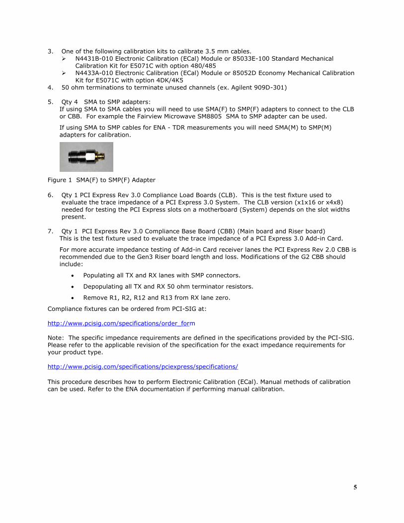
5. Qty 4 SMA to SMP adapters:
If using SMA to SMA cables you will need to use SMA(F) to SMP(F) adapters to connect to the CLB or CBB. For example the Fairview Microwave SM8805 SMA to SMP adapter can be used.
If using SMA to SMP cables for ENA - TDR measurements you will need SMA(M) to SMP(M)
adapters for calibration.
Figure 1 SMA(F) to SMP(F) Adapter
6. Qty 1 PCI Express Rev 3.0 Compliance Load Boards (CLB). This is the test fixture used to evaluate the trace impedance of a PCI Express 3.0 System. The CLB version (x1x16 or x4x8)
needed for testing the PCI Express slots on a motherboard (System) depends on the slot widths present.
7. Qty 1 PCI Express Rev 3.0 Compliance Base Board (CBB) (Main board and Riser board) This is the test fixture used to evaluate the trace impedance of a PCI Express 3.0 Add-in Card.
For more accurate impedance testing of Add-in Card receiver lanes the PCI Express Rev 2.0 CBB is recommended due to the Gen3 Riser board length and loss. Modifications of the G2 CBB should
include:
Populating all TX and RX lanes with SMP connectors.
Depopulating all TX and RX 50 ohm terminator resistors.
Remove R1, R2, R12 and R13 from RX lane zero.
Compliance fixtures can be ordered from PCI-SIG at:
http://www.pcisig.com/specifications/order_form Note: The specific impedance requirements are defined in the specifications provided by the PCI-SIG. Please refer to the applicable revision of the specification for the exact impedance requirements for your product type. http://www.pcisig.com/specifications/pciexpress/specifications/
This procedure describes how to perform Electronic Calibration (ECal). Manual methods of calibration can be used. Refer to the ENA documentation if performing manual calibration.
3 Measuring System Board PCB Trace Impedance: Calibration and Setup
Plug the ECal module into the ENA with the USB cable provided. Allow the ENA and the ECal module sufficient time to warm up. The ECal module green “Ready” light will come on when the ECal module is ready to work.
1. On the ENA, select the Setup button. 2. Select Setup Wizard 3. Select the “Full Calibration (ECal)” radio button and “Next”.
Figure 2 E5071C Network Analyzer Setup Wizard
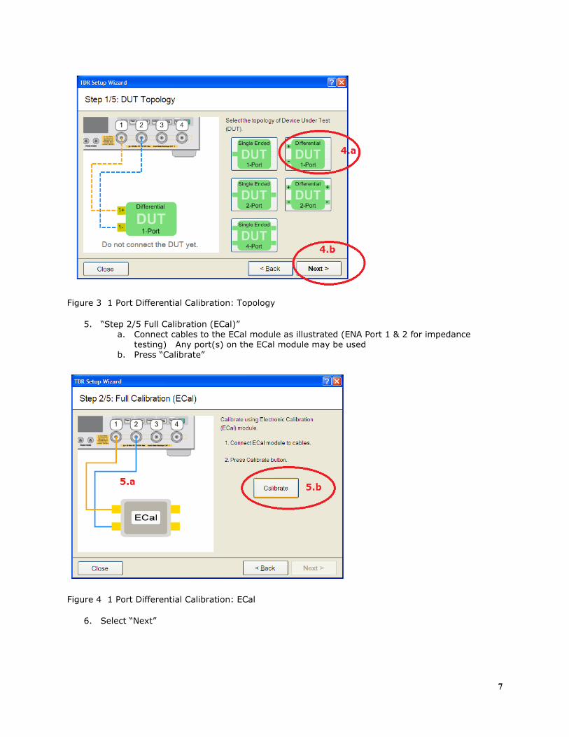
4. “Step: 1/5: DUT Topology”
a. Select “Differential 1-Port” b. Select ”Next” and “OK”
7
Figure 3 1 Port Differential Calibration: Topology
5. “Step 2/5 Full Calibration (ECal)” a. Connect cables to the ECal module as illustrated (ENA Port 1 & 2 for impedance
testing) Any port(s) on the ECal module may be used b. Press “Calibrate”
Figure 4 1 Port Differential Calibration: ECal
6. Select “Next”
ENA - TDR Test Procedure Document <0001> 8
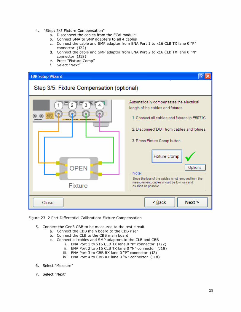
7. “Step: 3/5 Fixture Compensation”
a. Disconnect the cables from the ECal module b. Connect SMA to SMP adapters to the cables c. Connect the cables and SMP adapters to the CLB test fixture TX Lane 0
Do not connect a DUT d. Press Fixture Comp button e. Select “Next”
Figure 5 1 Port Differential Calibration: Fixture Compensation
Figure 6 CLB 3.0 x1x16 Test Fixture (TX side)
9
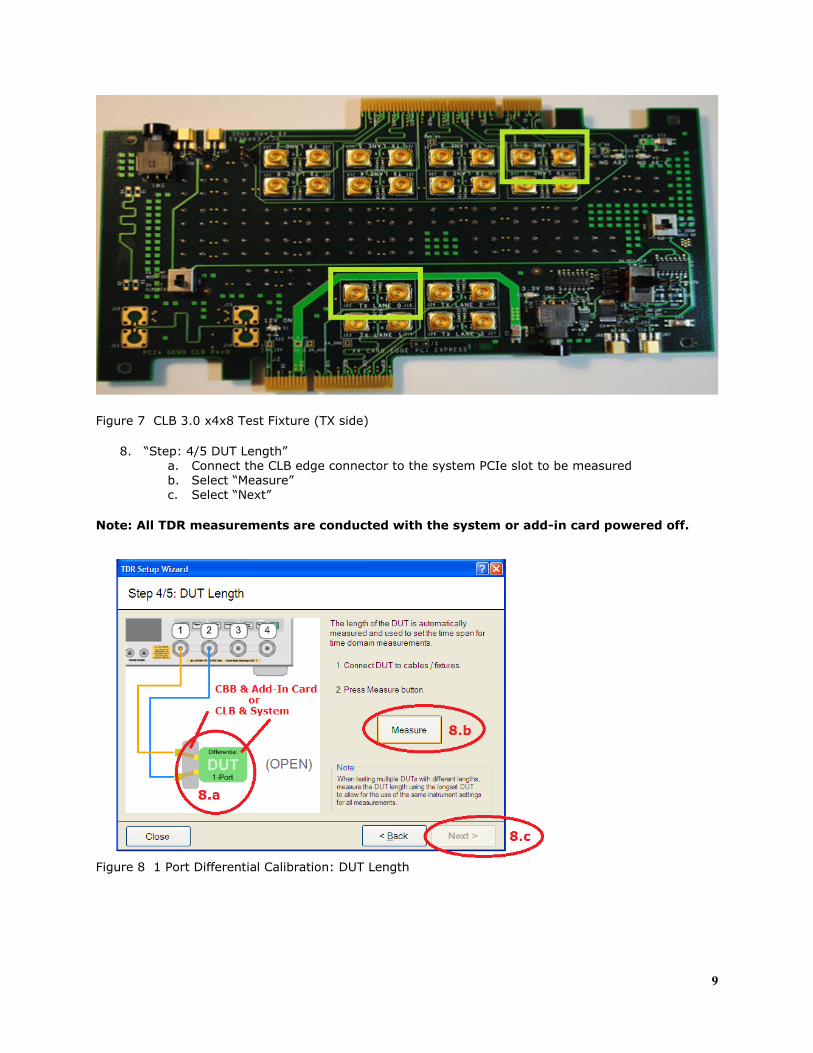
Figure 7 CLB 3.0 x4x8 Test Fixture (TX side)
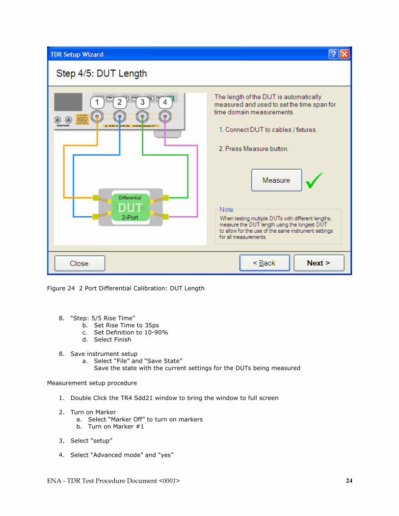
8. “Step: 4/5 DUT Length” a. Connect the CLB edge connector to the system PCIe slot to be measured b. Select “Measure” c. Select “Next”
Note: All TDR measurements are conducted with the system or add-in card powered off.
Figure 8 1 Port Differential Calibration: DUT Length
ENA - TDR Test Procedure Document <0001> 10
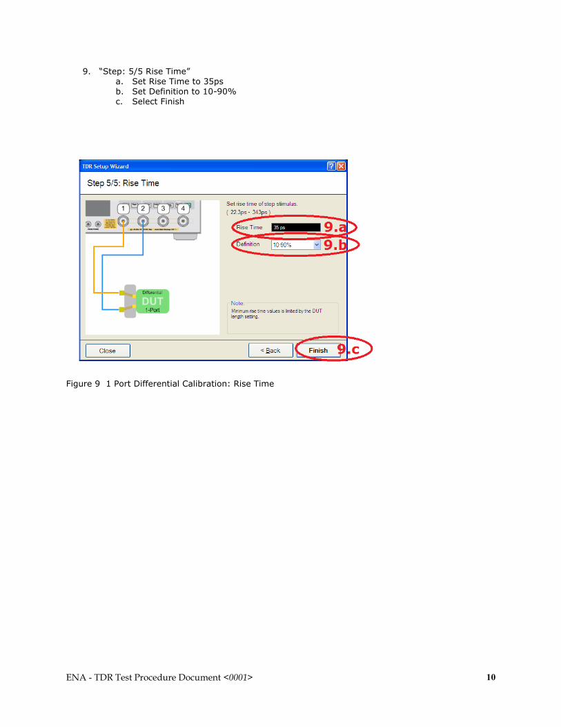
9. “Step: 5/5 Rise Time”
a. Set Rise Time to 35ps b. Set Definition to 10-90% c. Select Finish
Figure 9 1 Port Differential Calibration: Rise Time
11
10. Double click the Tr1 window to set TDR view
11. Set the Horizontal and Vertical resolution
a. Select “TDR/TDT”
1. Set Horizontal Resolution: 1 ns/div 2. Set Horizontal Position: -1 ns 3. Set Vertical Resolution: 5 Ohms/div 4. Set Vertical Position: 60 Ohms
Note: these values may be changed if needed to show the full DUT impedance trace. Set the Horizontal Resolution between 200ps/div and 1ns/div to place the open termination end of the DUT in
the right hand half of the Tr1 window.
Figure 10 TDR Horizontal and Vertical Resolution
ENA - TDR Test Procedure Document <0001> 12
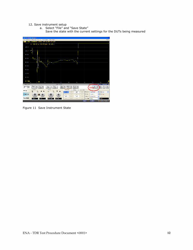
12. Save instrument setup
a. Select “File” and “Save State” Save the state with the current settings for the DUTs being measured
Figure 11 Save Instrument State
13
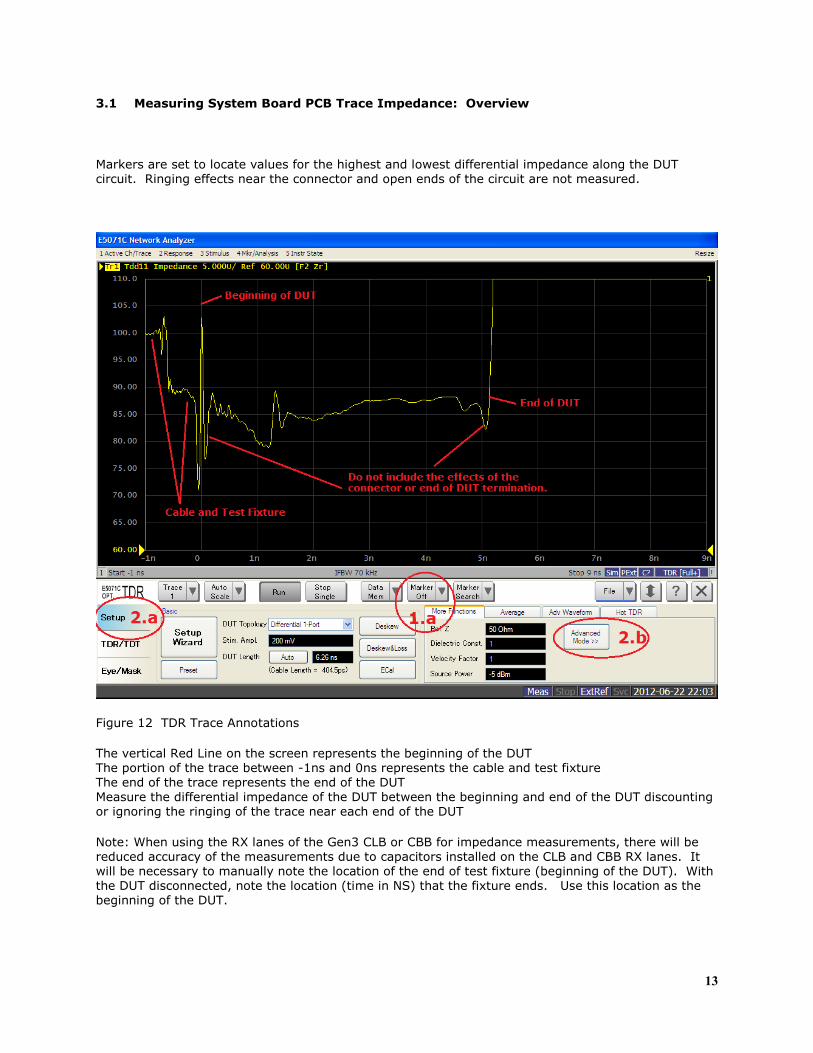
3.1 Measuring System Board PCB Trace Impedance: Overview
Markers are set to locate values for the highest and lowest differential impedance along the DUT circuit. Ringing effects near the connector and open ends of the circuit are not measured.
Figure 12 TDR Trace Annotations
The vertical Red Line on the screen represents the beginning of the DUT The portion of the trace between -1ns and 0ns represents the cable and test fixture The end of the trace represents the end of the DUT
Measure the differential impedance of the DUT between the beginning and end of the DUT discounting or ignoring the ringing of the trace near each end of the DUT
Note: When using the RX lanes of the Gen3 CLB or CBB for impedance measurements, there will be reduced accuracy of the measurements due to capacitors installed on the CLB and CBB RX lanes. It will be necessary to manually note the location of the end of test fixture (beginning of the DUT). With the DUT disconnected, note the location (time in NS) that the fixture ends. Use this location as the beginning of the DUT.
ENA - TDR Test Procedure Document <0001> 14
3.2 System Board Impedance Measurement
1. Turn on Markers a. Select “Marker Off” to turn on markers b. Turn on Marker #1
c. Turn on Marker #2
2. Set Marker Search a. Select “Setup” b. Select “Advanced Mode” and “yes” c. Select “Marker Search” d. Select “Search Range”
e. Set “Start” at 200ps f. Set “Stop” to end of trace minus 200ps Place a marker at the end of the DUT where the open impedance where the trace rises through 110 ohms. Subtract 200 ps from the time location of the marker and use the
calculated value for the gating “Stop” value. g. Toggle Search Range from “OFF” to “ON”
Figure 13 Advanced Mode Setup: Marker Search
15
Figure 14 Advanced Mode Setup: Search Range Values
3. Set Markers a. Highlight Marker 1 b. Select “Marker Search” and “Max” c. Highlight Marker 2 d. Select “Marker Search” and “Min”
Figure 15 Advanced Mode Setup: Set Markers
ENA - TDR Test Procedure Document <0001> 16
4. Measure DUT
a. Max value: Record DUT High Impedance (Marker 1) b. Min value: Record DUT Low Impedance (Marker 2)
8GT capable devices must have differential impedance between 70 ohms and 100 ohms
Device fails if Max value is higher than 100 ohms or Min value is below 70 ohms
5GT capable devices must have differential impedance between 65 and 105 ohm Device fails if Max value is higher than 105 ohms or min value is below 65 ohms
Note: In most cases, 200ps from each end of the DUT is adequate to remove connector and open end ringing effects. If high or low value falls on the gate locations due to connector or end effects, it may be necessary to adjust the gates a small amount.
5. Set Limit Line (Optional)
A limit line may be set to graphically illustrate a pass/fail line. A device under test fails if
any part of the PCB trace impedance crosses through the Limit Line. The portions of the trace that cross the limit line(s) will appear colored red. Exceptions are made for violations due to connectors, via’s or any components in the signal path. In exception cases the user must manually determine the exception location and measure the result manually to determine pass/fail status.
a. Select “Analysis” b. Select “Limit Test” c. Select “Edit Limit Line” d. Edit limit as shown in figure (set to the values determined in step 4. above) e. Turn on “Limit Line” and “Limit Test”
Figure 16 Setup Limit Line
17
Figure 17 Input limit values
--
Figure 18 Limit Line view
ENA - TDR Test Procedure Document <0001> 18
4 Add-In Card PCB Trace Impedance Measurement: Calibration and Setup
Note: Refer to section 3 (System Board PCB Impedance: Calibration and Setup) and modify the procedures as instructed below.
1. Perform steps in section 3 (System Board PCB Impedance: Calibration and Setup) step 1
through step 6.
Figure 19 CBB 3.0 Test Fixture Riser
Figure 20 CBB 3.0 Test Fixture Main board
19
2. “Step: 3/5 Fixture Compensation”
a. Connect the CBB 3.0 main board to the CBB riser b. Disconnect the cables from the ECal module c. Connect SMA to SMP adapters to the cables
d. Connect the cables and SMP adapters to the CBB test fixture TX Lane 0 Do not connect a DUT
e. Press Fixture Comp button f. Select “Next”
3. “Step: 4/5 DUT Length”
a. Insert Add-In Card in the CBB PCIe connector
b. Select “Measure” c. Select “Next”
Note: All TDR measurements are conducted with the system or add-in card powered off.
4. Perform steps in section 3 (System Board PCB Impedance: Calibration and Setup) step 9 through step 11.
2. Perform steps in section 3.2 (Measurement setup procedure) step 1 through step 3
3. Measure DUT a. Max value: Record DUT High Impedance (Marker 1)
b. Min value: Record DUT Low Impedance (Marker 2)
8GT capable devices must have differential impedance between 70 ohms and 100 ohms Device fails if Max value is higher than 100 ohms or Min value is below 70 ohms
5GT capable devices must have differential impedance between 65 and 105 ohm Device fails if Max value is higher than 105 ohms or min value is below 65 ohms
Note: In most cases, 200ps from each end of the DUT is adequate to remove connector and open end ringing effects. If high or low value falls on the gate locations due to connector or end effects, it may be necessary to adjust the gates a small amount.
6. Set Limit Line (Optional) A limit line may be set to graphically illustrate a pass/fail line. A device under test fails if any part of the PCB trace impedance crosses through the Limit Line. The portions of the
trace that cross the limit line(s) will appear colored red. Exceptions are made for violations due to connectors, via’s or any components in the signal path. In exception cases the user must manually determine the exception location and measure the result manually to
determine pass/fail status.
a. Follow instructions in section 3.2, step 5. (above)
ENA - TDR Test Procedure Document <0001> 20
5 Measuring CBB and CLB Differential Lane Impedance
This section verifies that the differential impedance of the Compliance Base Board (CBB) and Compliance Load Board (CLB) TX and RX signal lanes are within the max min range specified.
1. Perform the steps in section 3 (System Board PCB Impedance: Calibration and Setup) step 1 through step 6.
2. Section 3 -Step 7 (Step: 3/5 Fixture Compensation) Perform all steps up through step b. (b. Connect SMA to SMP adapters to the cables) Do not connect CLB or CBB to the cables
Continue with step d. (Press Fixture Comp button)
3. Section 3 -Step 8 (Step: 4/5 DUT Length) Step a. (Connect the DUT with the longest circuit to be measured to the test fixture)
Connect the TX lane 0 of a CLB or CBB to the cables and SMP adapters (The CLB or CBB is now the “DUT”)
Continue with step b. (Select “Measure”)
4. Complete the steps in Section 3 step 9 through step 12 (Save State)
5. Perform steps in section 3.2 (Measurement setup procedure) step 1 through step 3 except as follows
a. Set the Search Range “Start” value to 100ps
b. Set the Search Range “Stop” value to end of DUT minus 100ps c. Complete all steps through “Measure DUT” d. Move the cables to each TX lane and record differential impedance for each lane
6. It is necessary to turn off gating to measure differential impedance of the RX lanes
a. Connect the cables to RX lane 0 b. Toggle Gating on/off to “off”
c. Manually place the markers to the max and min location of the DUT trace d. Move the cables to each RX lane and record differential impedance for each lane
21
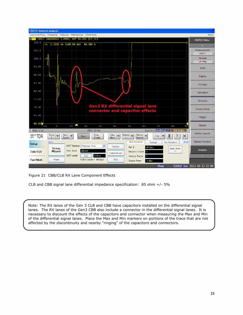
Figure 21 CBB/CLB RX Lane Component Effects
CLB and CBB signal lane differential impedance specification: 85 ohm +/- 5%
Note: The RX lanes of the Gen 3 CLB and CBB have capacitors installed on the differential signal lanes. The RX lanes of the Gen3 CBB also include a connector in the differential signal lanes. It is necessary to discount the effects of the capacitors and connector when measuring the Max and Min of the differential signal lanes. Place the Max and Min markers on portions of the trace that are not
affected by the discontinuity and nearby “ringing” of the capacitors and connectors.
ENA - TDR Test Procedure Document <0001> 22
6 Insertion Loss Measurements CBB and CLB signal circuits
This section describes a procedure to measure the insertion loss of the CLB TX connected to the CBB RX differential signal circuits to assure the insertion loss is within the specified range. This procedure may be used as an example to measure 2 port differential circuits that have test points accessible on
each end of the differential circuit.
Plug the ECal module into the ENA with the USB cable provided. Allow the ENA and the ECal module sufficient time to warm up. The ECal module green “Ready” light will come on when the ECal module is ready to work.
1. On the ENA, select the Setup button. 2. Select Setup Wizard 3. Select the “Full Calibration (ECal)” radio button and “Next”
4. “Step: 1/5: DUT Topology”
a. Select “Differential 2-Port” b. Select ”Next” and “OK”
Figure 22 2 Port Differential Calibration: Topology
5. “Step 2/5 Full Calibration (ECal)”
a. Connect 4 cables to the ECal module as illustrated b. Press “Calibrate”
23
4. “Step: 3/5 Fixture Compensation”
a. Disconnect the cables from the ECal module b. Connect SMA to SMP adapters to all 4 cables c. Connect the cable and SMP adapter from ENA Port 1 to x16 CLB TX lane 0 “P”
connector (J22) d. Connect the cable and SMP adapter from ENA Port 2 to x16 CLB TX lane 0 “N”
connector (J18) e. Press “Fixture Comp” f. Select “Next”
Figure 23 2 Port Differential Calibration: Fixture Compensation
5. Connect the Gen3 CBB to be measured to the test circuit a. Connect the CBB main board to the CBB riser
b. Connect the CLB to the CBB main board c. Connect all cables and SMP adaptors to the CLB and CBB
i. ENA Port 1 to x16 CLB TX lane 0 “P” connector (J22) ii. ENA Port 2 to x16 CLB TX lane 0 “N” connector (J18) iii. ENA Port 3 to CBB RX lane 0 “P” connector (J2) iv. ENA Port 4 to CBB RX lane 0 “N” connector (J18)
6. Select “Measure”
7. Select “Next”
ENA - TDR Test Procedure Document <0001> 24
Figure 24 2 Port Differential Calibration: DUT Length
8. “Step: 5/5 Rise Time” b. Set Rise Time to 35ps c. Set Definition to 10-90% d. Select Finish
8. Save instrument setup a. Select “File” and “Save State”
Save the state with the current settings for the DUTs being measured
Measurement setup procedure
1. Double Click the TR4 Sdd21 window to bring the window to full screen
2. Turn on Marker
a. Select “Marker Off” to turn on markers b. Turn on Marker #1
3. Select “setup”
4. Select “Advanced mode” and “yes”
25
5. Select “Marker” a. Select “Marker 1” and set to 4GHz
Figure 25 Advanced Mode Setup: Set Insertion Loss Marker
6. Record the Insertion Loss value at 4GHz
7. For all lanes to be measured, connect ENA Ports 1 & 2 to the respective TX lanes “P” and “N” connectors and ENA Ports 3 & 4 2 to the respective RX lanes “P” and “N” connectors. If taking repeated measurements, confirm that Marker 1 is set at the proper frequency with each recording.
Note: 4 GHz correlates to the fundamental frequency used for 8GT signaling. The insertion loss can also be measured at 2.5 GHz for the fundamental frequency used for 5GT signaling. To measure the insertion loss of the CBB TX connected to the CLB RX differential signal circuit, repeat the complete procedure exchanging CBB TX lanes in place of the CLB TX lanes and CLB RX lanes in
place of the CBB RX lanes.
Acceptance criteria for CLB's and CBB's Insertion loss at 4GHz* 1. CBB RX lanes measured through (including) CLB TX:
Measured Insertion Loss between -14.0dB and -15.5dB 2. CLB RX lanes measured through (including) CBB TX lanes:
Measured Insertion Loss between -7.0dB and -8.5dB
*Measured Insertion Loss includes the contribution of both the RX and TX lane and low loss SMA to SMP adapters. The affect (loss) of the test cables has been calibrated out of the measured values. Measurements taken in environmentally controlled lab conditions near 70 deg. f. and moderate humidity levels.
ENA - TDR Test Procedure Document <0001> 26
Figures
Figure 1 SMA(F) to SMP(F) Adapter ....................................................... 5