33
PCIe standard updates and 3.0 testing challenges Gordon Getty Russ McHugh Agilent Technologies © Agilent Technologies, 2012
PCIe standard updates
and 3.0 testing
challenges
Gordon Getty
Russ McHugh
Agilent Technologies
© Agilent Technologies, 2012
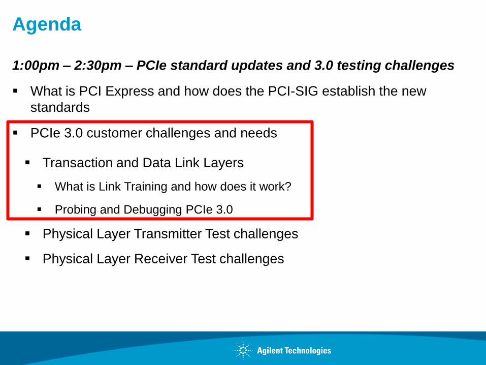
Agenda
1:00pm – 2:30pm – PCIe standard updates and 3.0 testing challenges
What is PCI Express and how does the PCI-SIG establish the new
standards
PCIe 3.0 customer challenges and needs
Transaction and Data Link Layers
What is Link Training and how does it work?
Probing and Debugging PCIe 3.0
Physical Layer Transmitter Test challenges
Physical Layer Receiver Test challenges
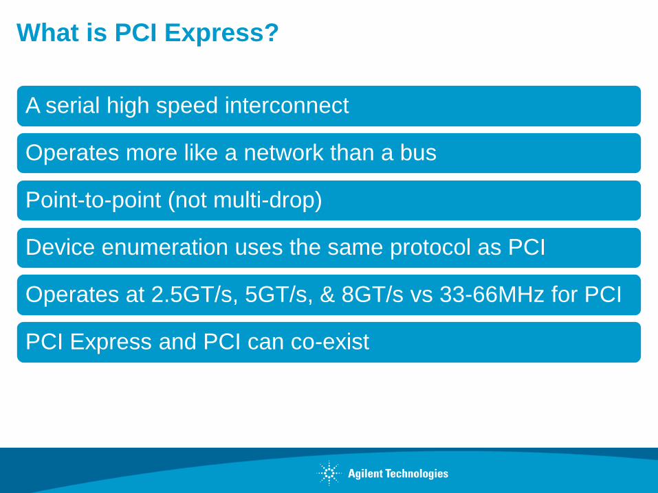
What is PCI Express?
A serial high speed interconnect
Operates more like a network than a bus
Point-to-point (not multi-drop)
Device enumeration uses the same protocol as PCI
Operates at 2.5GT/s, 5GT/s, & 8GT/s vs 33-66MHz for PCI
PCI Express and PCI can co-exist
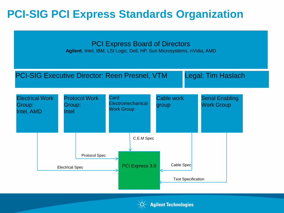
PCI-SIG PCI Express Standards Organization
PCI Express Board of Directors Agilent, Intel, IBM, LSI Logic, Dell, HP, Sun Microsystems, nVidia, AMD
PCI-SIG Executive Director: Reen Presnel, VTM
Electrical Work
Group:
Intel, AMD
Protocol Work
Group:
Intel
Card
Electromechanical
Work Group
Cable work
group
Legal: Tim Haslach
PCI Express 3.0
Serial Enabling
Work Group
Electrical Spec
Protocol Spec
C.E.M Spec
Cable Spec
Test Specification
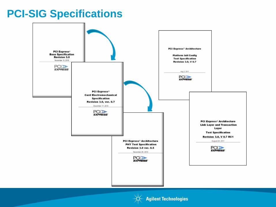
PCI-SIG Specifications
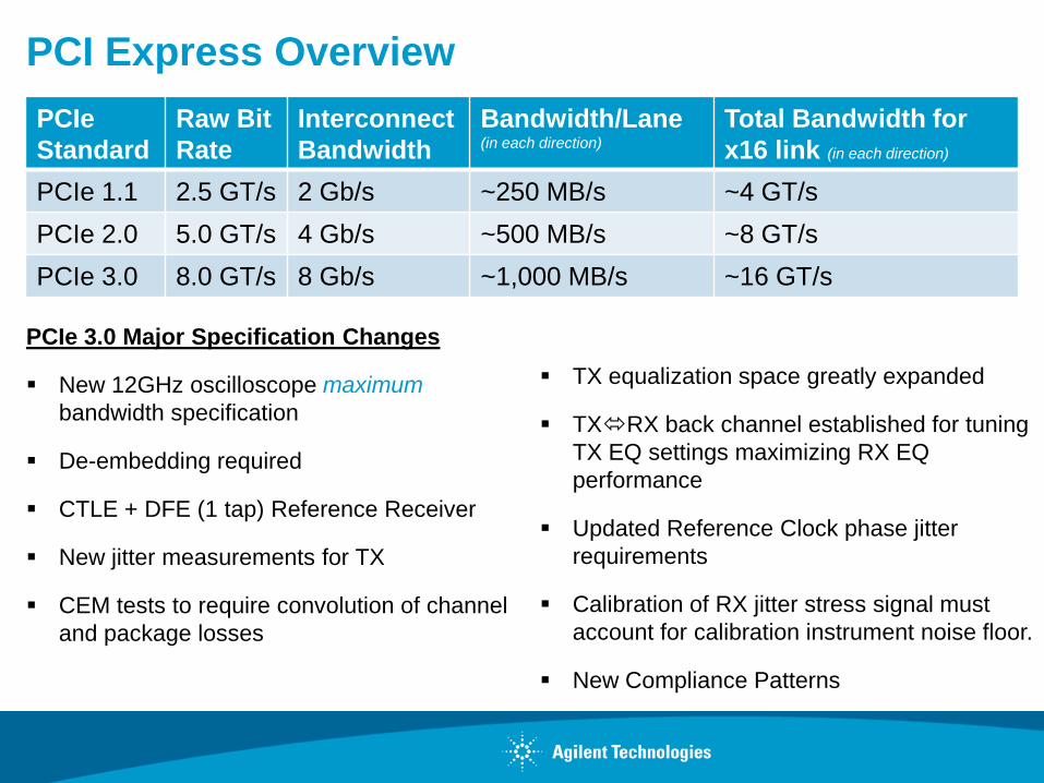
PCI Express Overview
PCIe
Standard
Raw Bit
Rate
Interconnect
Bandwidth
Bandwidth/Lane (in each direction)
Total Bandwidth for
x16 link (in each direction)
PCIe 1.1 2.5 GT/s 2 Gb/s ~250 MB/s ~4 GT/s
PCIe 2.0 5.0 GT/s 4 Gb/s ~500 MB/s ~8 GT/s
PCIe 3.0 8.0 GT/s 8 Gb/s ~1,000 MB/s ~16 GT/s
PCIe 3.0 Major Specification Changes
New 12GHz oscilloscope maximum
bandwidth specification
De-embedding required
CTLE + DFE (1 tap) Reference Receiver
New jitter measurements for TX
CEM tests to require convolution of channel
and package losses
TX equalization space greatly expanded
TXRX back channel established for tuning
TX EQ settings maximizing RX EQ
performance
Updated Reference Clock phase jitter
requirements
Calibration of RX jitter stress signal must
account for calibration instrument noise floor.
New Compliance Patterns
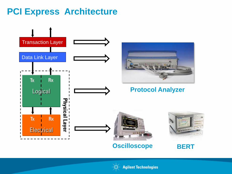
PCI Express Architecture
Logical
Electrical
Tx Rx
Tx Rx
Physic
al L
aye
r
Transaction Layer
Data Link Layer
Protocol Analyzer
BERT Oscilloscope
Agenda
1:00pm – 2:30pm – PCIe standard updates and 3.0 testing challenges
What is PCI Express and how does the PCI-SIG establish the new
standards
PCIe 3.0 customer challenges and needs
Transaction and Data Link Layers
What is Link Training and how does it work?
Probing and Debugging PCIe 3.0
Physical Layer Transmitter Test challenges
Physical Layer Receiver Test challenges
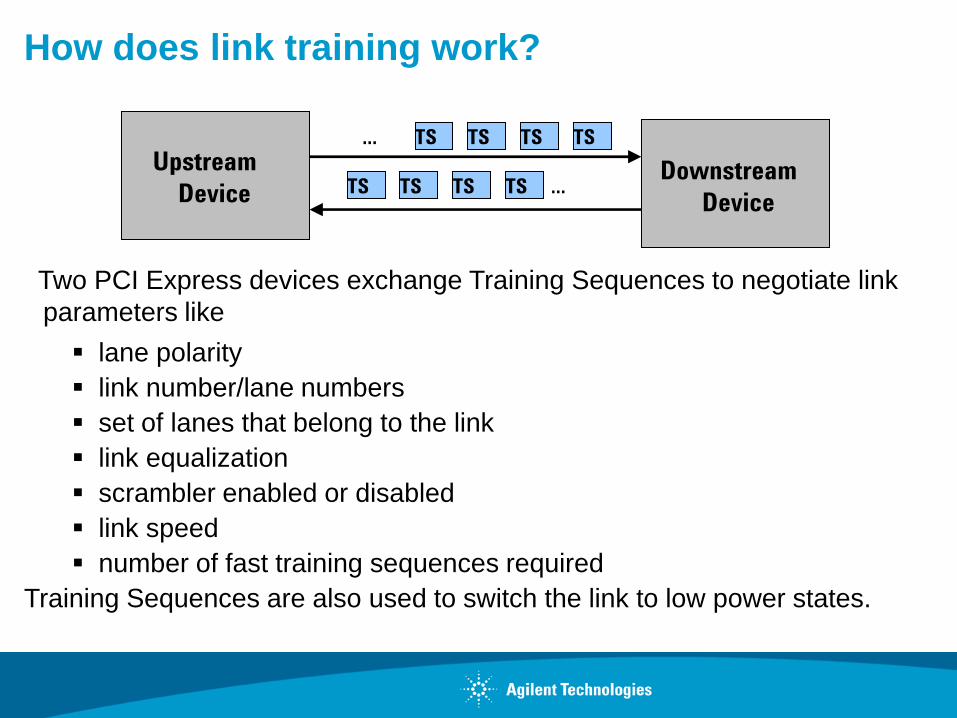
Two PCI Express devices exchange Training Sequences to negotiate link
parameters like
lane polarity
link number/lane numbers
set of lanes that belong to the link
link equalization
scrambler enabled or disabled
link speed
number of fast training sequences required
Training Sequences are also used to switch the link to low power states.
How does link training work?
Upstream
Device Downstream
Device
TS TS TS TS ...
TS TS TS TS ...
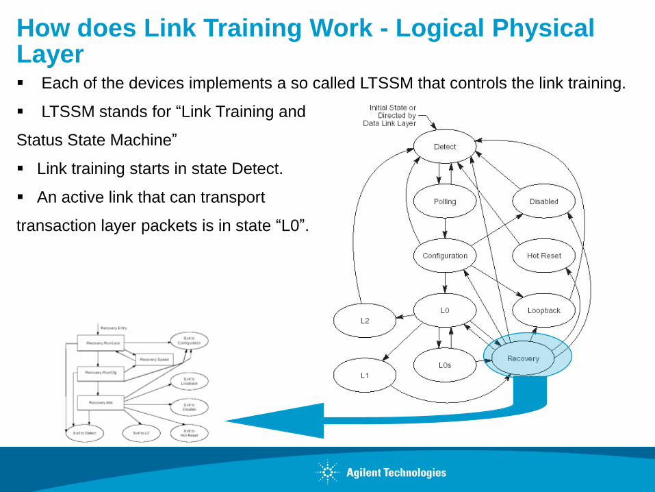
How does Link Training Work - Logical Physical Layer Each of the devices implements a so called LTSSM that controls the link training.
LTSSM stands for “Link Training and
Status State Machine”
Link training starts in state Detect.
An active link that can transport
transaction layer packets is in state “L0”.
Debugging Equalization Problems
Which phase of equalization does the link get to?
Does the link get to 8G with equalization disabled
Change the presets and coefficients that are being used
Check BIOS settings on platform
Monitoring the rate of Recovery state transitions in L0 may give
an indicator if frame errors are happening
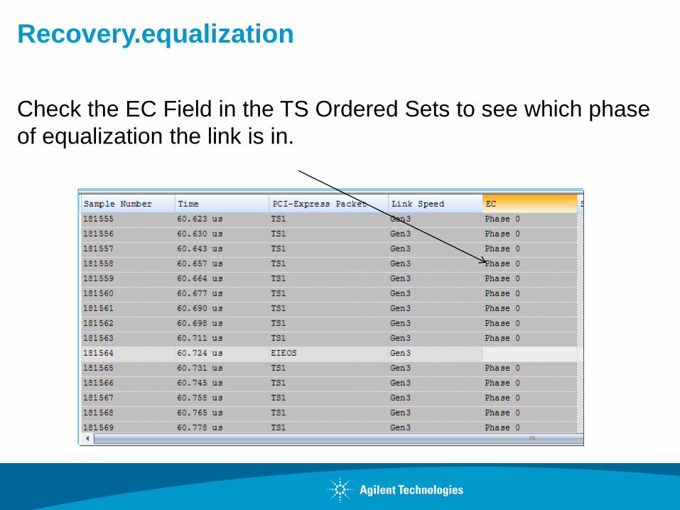
Recovery.equalization
Check the EC Field in the TS Ordered Sets to see which phase
of equalization the link is in.
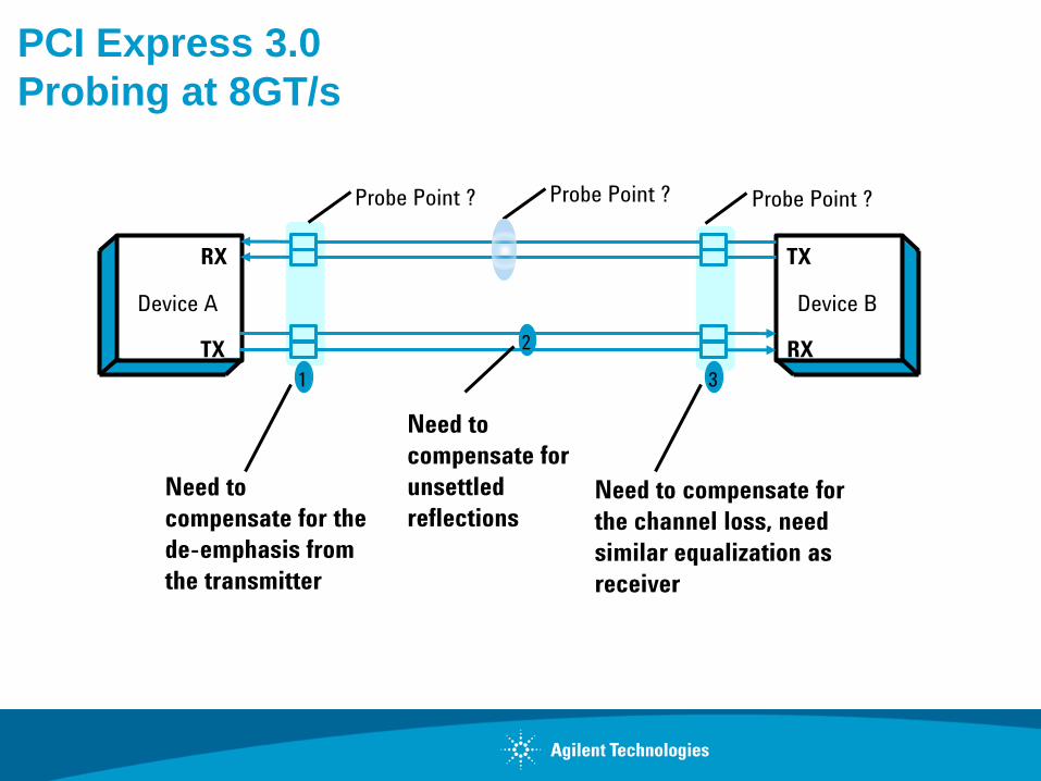
PCI Express 3.0
Probing at 8GT/s
Probe Point ?
1 3
Device B Device A
RX
RX TX
TX
Need to
compensate for the
de-emphasis from
the transmitter
Need to compensate for
the channel loss, need
similar equalization as
receiver
Probe Point ? Probe Point ?
2
Need to
compensate for
unsettled
reflections
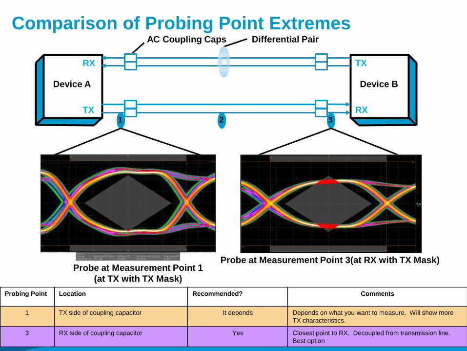
Comparison of Probing Point Extremes Differential Pair AC Coupling Caps
1 2 3
Probe at Measurement Point 3(at RX with TX Mask) Probe at Measurement Point 1
(at TX with TX Mask)
Device B Device A
RX
RX TX
TX
Probing Point Location Recommended? Comments
1 TX side of coupling capacitor
It depends Depends on what you want to measure. Will show more
TX characteristics.
3 RX side of coupling capacitor
Yes Closest point to RX. Decoupled from transmission line.
Best option
Tools required for debugging
Debugging PCI Express 3.0 designs is complex
Isolate the layer that the problem occurs
Thorough validation of the physical layer will prevent physical
layer problems causing Link Training and Transaction Layer
problems
Using the correct tool will ease debug
Agenda
1:00pm – 2:30pm – PCIe standard updates and 3.0 testing challenges
What is PCI Express and how does the PCI-SIG establish the new
standards
PCIe 3.0 customer challenges and needs
Transaction and Data Link Layers
What is Link Training and how does it work?
Probing and Debugging PCIe 3.0
Physical Layer Transmitter Test challenges
Physical Layer Receiver Test challenges
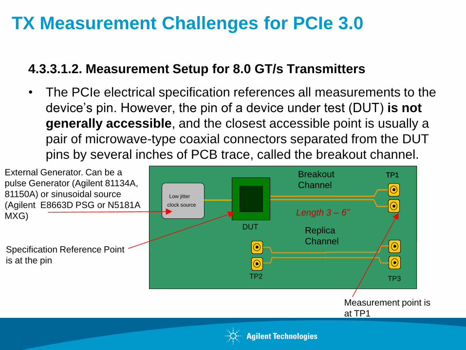
TX Measurement Challenges for PCIe 3.0
4.3.3.1.2. Measurement Setup for 8.0 GT/s Transmitters
• The PCIe electrical specification references all measurements to the
device‟s pin. However, the pin of a device under test (DUT) is not
generally accessible, and the closest accessible point is usually a
pair of microwave-type coaxial connectors separated from the DUT
pins by several inches of PCB trace, called the breakout channel.
DUT
Low jitter
clock source
TP1 TP1
DUT
Breakout
Channel Low jitter
clock source
TP3 TP2
Replica
Channel
Length 3 – 6”
External Generator. Can be a
pulse Generator (Agilent 81134A,
81150A) or sinusoidal source
(Agilent E8663D PSG or N5181A
MXG)
Specification Reference Point
is at the pin
Measurement point is
at TP1
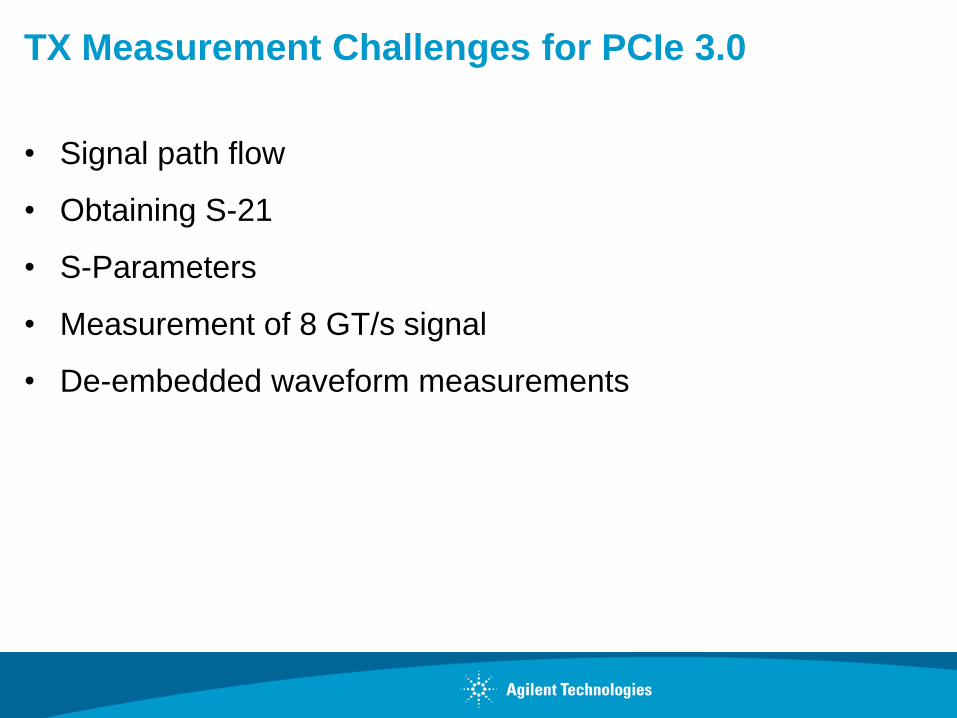
TX Measurement Challenges for PCIe 3.0
• Signal path flow
• Obtaining S-21
• S-Parameters
• Measurement of 8 GT/s signal
• De-embedded waveform measurements
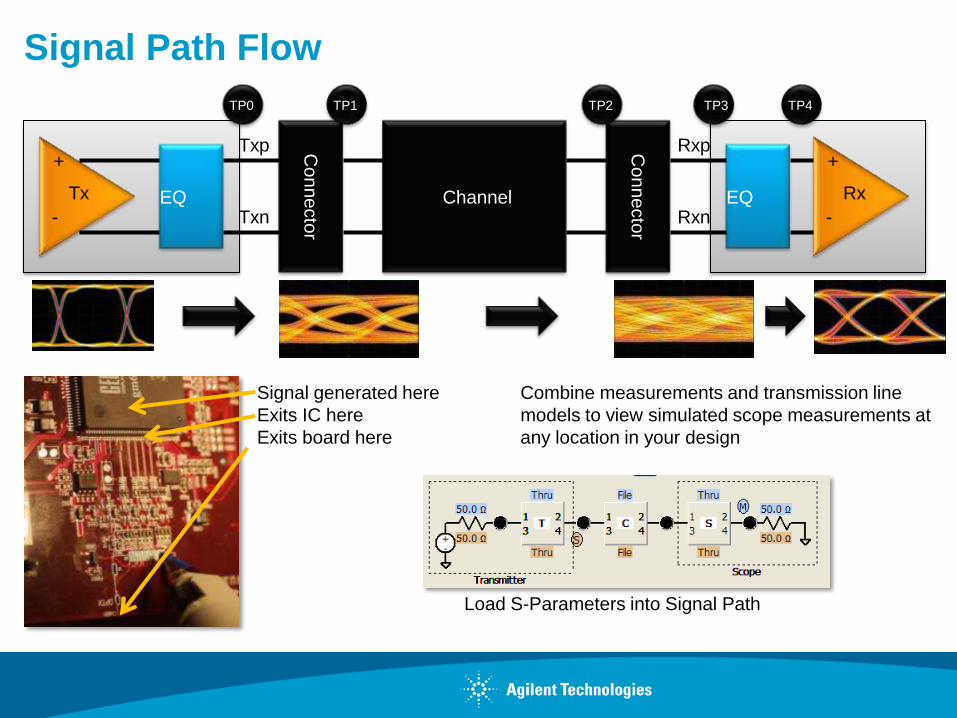
Signal Path Flow
EQ
+
-
Co
nn
ecto
r
TP0 TP1
Channel
Co
nn
ecto
r
EQ
+
-
TP2 TP3 TP4
Txp
Txn Rxn
Rxp
Tx Rx
Signal generated here
Exits IC here
Exits board here
Combine measurements and transmission line
models to view simulated scope measurements at
any location in your design
Load S-Parameters into Signal Path
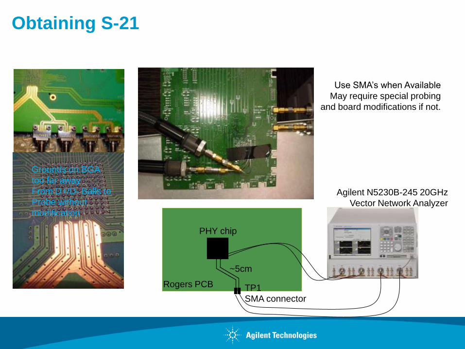
Obtaining S-21
TP1
SMA connector
Rogers PCB
PHY chip
~5cm
Agilent N5230B-245 20GHz
Vector Network Analyzer
Use SMA‟s when Available
May require special probing
and board modifications if not.
Grounds on BGA
too far away
From D+/D- Balls to
Probe without
modification
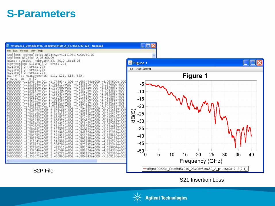
S-Parameters
S2P File
S21 Insertion Loss
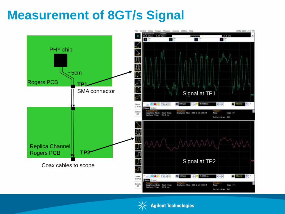
Measurement of 8GT/s Signal
Signal at TP2 Coax cables to scope
TP1
SMA connector
Rogers PCB
PHY chip
~5cm
Replica Channel
Rogers PCB TP2
Signal at TP1
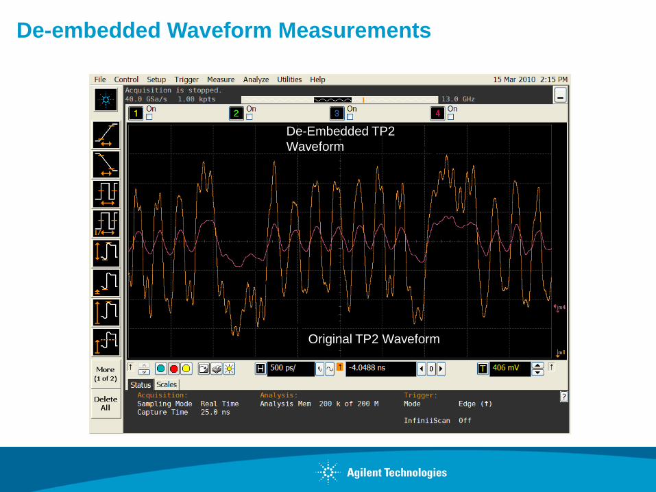
De-embedded Waveform Measurements
Original TP2 Waveform
De-Embedded TP2
Waveform
Agenda
1:00pm – 2:30pm – PCIe standard updates and 3.0 testing challenges
What is PCI Express and how does the PCI-SIG establish the new
standards
PCIe 3.0 customer challenges and needs
Transaction and Data Link Layers
What is Link Training and how does it work?
Probing and Debugging PCIe 3.0
Physical Layer Transmitter Test challenges
Physical Layer Receiver Test challenges
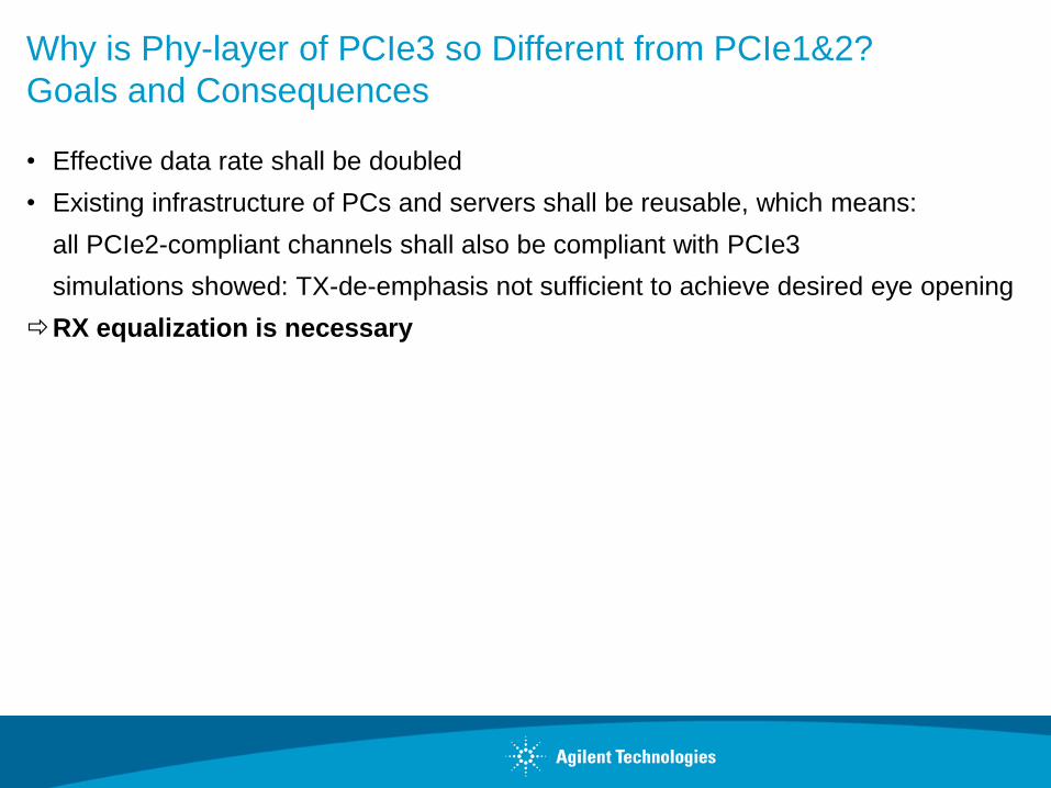
Why is Phy-layer of PCIe3 so Different from PCIe1&2?
Goals and Consequences
• Effective data rate shall be doubled
• Existing infrastructure of PCs and servers shall be reusable, which means:
all PCIe2-compliant channels shall also be compliant with PCIe3
simulations showed: TX-de-emphasis not sufficient to achieve desired eye opening
RX equalization is necessary
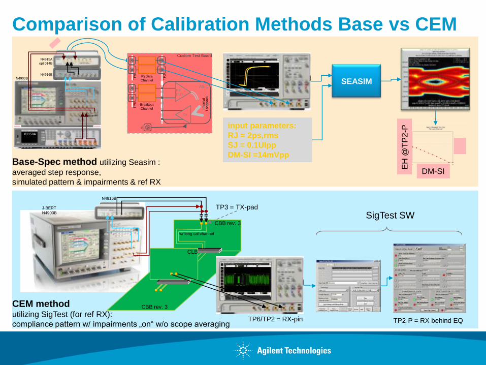
Base-Spec method utilizing Seasim :
averaged step response,
simulated pattern & impairments & ref RX
CEM method utilizing SigTest (for ref RX):
compliance pattern w/ impairments „on“ w/o scope averaging
N4916B
N4915A
opt 014B
N4903B
81150A
CBB rev. 3
w/ long cal channel
CBB rev. 3
CLB
N4916B
J-BERT
N4903B
SEASIM
DM-SI
EH
@T
P2
-P
Custom Test Board
TP
2
Breakout
Channel
Ref
Clk
TP
6
Replica
Channel TP
5
ASIC RX
DUT
TX
Inte
rnal
Loopback
Comparison of Calibration Methods Base vs CEM
TP3 = TX-pad
TP6/TP2 = RX-pin TP2-P = RX behind EQ
input parameters:
RJ = 2ps,rms
SJ = 0.1UIpp
DM-SI =14mVpp
SigTest SW
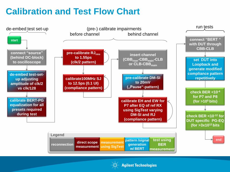
Calibration and Test Flow Chart
calibrate BERT-PG
equalization for all
presets required
during test
pre-calibrate RJrms
to 1.55ps
(clk/2 pattern)
start
de-embed test-set-
up adjusting
amplitude of clk/2
vs clk/128
calibrate100MHz SJ
to 12.5ps (0.1 UI)
(compliance pattern)
pre-calibrate DM-SI
to 20mV
(„Pause“-pattern)
de-embed test set-up (pre-) calibrate impairments
before channel behind channel
insert channel
(CBBriser-CBBmain-CLB
or CLB-CBBmain
connect “source”
(behind DC-block)
to oscilloscope
calibrate EH and EW for
P7 after EQ of ref RX
using SigTest varying
DM-SI and RJ
(compliance pattern)
set DUT into
Loopback and
generate modified
compliance pattern
repetitively
connect “BERT “
with DUT through
CBB-CLB
check BER <10-4
for P7 and P8
(for >105 bits)
check BER <10-12 for
DUT specific PG-EQ
(for >3x1012 bits
end
Legend
pattern /signal
generation
w/ BERT
measurement
using SigTest reconnection
direct scope
measurement
test using
BER
measurement
run tests
Calibration of Jitter Value or Eye Opening
using SigTest-SW
The calibration procedure for any jitter value RJ, SJ (TJ) or eye opening (EH & EW) always consists of the following steps:
1. Set start value on J-BERT
2. Save waveform on DSA in bin format
3. Upload waveform to SigTest and calculate signal parameters using appropriate “Technology“ and “Template“ pressing <Test> button
4. If relevant result is out of target window adjust parameter on J-BERT accordingly and repeat procedure from 2.
5. Otherwise record value for later use
Note: DM-SI is determined w/o SigTest-SW by direct scope measurement
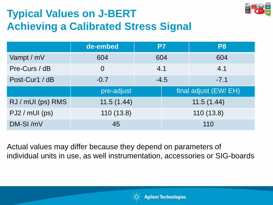
Typical Values on J-BERT
Achieving a Calibrated Stress Signal
de-embed P7 P8
Vampt / mV 604 604 604
Pre-Curs / dB 0 4.1 4.1
Post-Cur1 / dB -0.7 -4.5 -7.1
pre-adjust final adjust (EW/ EH)
RJ / mUI (ps) RMS 11.5 (1.44) 11.5 (1.44)
PJ2 / mUI (ps) 110 (13.8) 110 (13.8)
DM-SI /mV 45 110
Actual values may differ because they depend on parameters of
individual units in use, as well instrumentation, accessories or SIG-boards
calibrate BERT-PG
equalization for all
presets required during
test
pre-calibrate RJrms
to 1.55ps
start
de-embed test-set-up
adjusting amplitude of
clk/2
vs clk/128
calibrate100MHz SJ to
12.5ps (0.1 UI)
pre-calibrate DM-SI
to 20mV
de-embed test set-up (pre-) calibrate impairments
before channel behind channel
insert channel
(CBBriser-CBBmain-CLB
or CLB-CBBmain
connect “source”
(behind DC-block)
to scope
calibrate EH and EW for P7
after EQ of ref RX using
SigTest varying DM-SI and
RJ
set DUT into Loopback
and generate modified
compliance pattern
repetitively
connect “BERT with
DUT through CBB-CLB
check BER <10-4
for P7 and P8
(for >105 bits)
check BER <10-12 for
DUT specific PG-EQ
(for >3x1012 bits
end
run tests
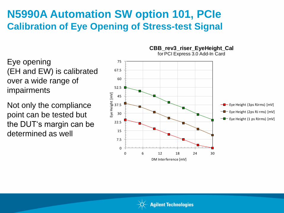
N5990A Automation SW option 101, PCIe Calibration of Eye Opening of Stress-test Signal
Eye opening
(EH and EW) is calibrated
over a wide range of
impairments
Not only the compliance
point can be tested but
the DUT„s margin can be
determined as well
0
7.5
15
22.5
30
37.5
45
52.5
60
67.5
75
0 6 12 18 24 30
Eye
He
igh
t [m
V]
DM Interference [mV]
CBB_rev3_riser_EyeHeight_Calfor PCI Express 3.0 Add-In Card
Eye Height (3ps RJrms) [mV]
Eye Height (2ps RJ rms) [mV]
Eye Height (1 ps RJrms) [mV]
Conclusions
1. Probing at pins of device not practical at PCIe 3.0 speeds of 8GT/s.
2. De-embedding may remove fixture effects and recover some jitter margin.
3. Voltage measurements more impacted by de-embedding noise compared to jitter.
4. Calibration of the stressed eye for receiver test should minimize effect of instrument noise.
5. Stressed eye for RX testing is referenced to the die pad for the receiver. TX voltage and jitter parameters are generally referenced to the pin of the device.
6. Calibration Channel is crucial for ensuring RX signal amplitudes are at the proper level at the RX Die pad.
7. CEM RX Test Calibration still TBD but should be ready by April workshop in Milpitas
8. Tools for full PCIe 3.0 TX and RX testing are available today.

Thank you!
Questions?


